EP1443597A1 - Antenne und Funkgerät mit einer derartigen Antenne - Google Patents
Antenne und Funkgerät mit einer derartigen Antenne Download PDFInfo
- Publication number
- EP1443597A1 EP1443597A1 EP04002170A EP04002170A EP1443597A1 EP 1443597 A1 EP1443597 A1 EP 1443597A1 EP 04002170 A EP04002170 A EP 04002170A EP 04002170 A EP04002170 A EP 04002170A EP 1443597 A1 EP1443597 A1 EP 1443597A1
- Authority
- EP
- European Patent Office
- Prior art keywords
- antenna
- antenna element
- antenna device
- base member
- shaped
- Prior art date
- Legal status (The legal status is an assumption and is not a legal conclusion. Google has not performed a legal analysis and makes no representation as to the accuracy of the status listed.)
- Granted
Links
- 238000004891 communication Methods 0.000 title claims description 22
- 239000003989 dielectric material Substances 0.000 claims abstract description 15
- 230000002093 peripheral effect Effects 0.000 claims description 14
- 230000003071 parasitic effect Effects 0.000 claims description 12
- 239000004020 conductor Substances 0.000 abstract description 50
- 229910052751 metal Inorganic materials 0.000 abstract description 17
- 239000002184 metal Substances 0.000 abstract description 17
- 238000000059 patterning Methods 0.000 abstract description 11
- 239000000758 substrate Substances 0.000 description 10
- 238000000034 method Methods 0.000 description 8
- 239000011347 resin Substances 0.000 description 4
- 229920005989 resin Polymers 0.000 description 4
- 230000005540 biological transmission Effects 0.000 description 3
- 239000000919 ceramic Substances 0.000 description 3
- KRHYYFGTRYWZRS-UHFFFAOYSA-M Fluoride anion Chemical compound [F-] KRHYYFGTRYWZRS-UHFFFAOYSA-M 0.000 description 2
- 229920000122 acrylonitrile butadiene styrene Polymers 0.000 description 2
- 239000011810 insulating material Substances 0.000 description 2
- 238000004519 manufacturing process Methods 0.000 description 2
- 239000011295 pitch Substances 0.000 description 2
- 238000007747 plating Methods 0.000 description 2
- 238000009877 rendering Methods 0.000 description 2
- 229910052709 silver Inorganic materials 0.000 description 2
- 239000004332 silver Substances 0.000 description 2
- JYEUMXHLPRZUAT-UHFFFAOYSA-N 1,2,3-triazine Chemical compound C1=CN=NN=C1 JYEUMXHLPRZUAT-UHFFFAOYSA-N 0.000 description 1
- RYGMFSIKBFXOCR-UHFFFAOYSA-N Copper Chemical compound [Cu] RYGMFSIKBFXOCR-UHFFFAOYSA-N 0.000 description 1
- 229920000106 Liquid crystal polymer Polymers 0.000 description 1
- 239000004977 Liquid-crystal polymers (LCPs) Substances 0.000 description 1
- 239000004642 Polyimide Substances 0.000 description 1
- GWEVSGVZZGPLCZ-UHFFFAOYSA-N Titan oxide Chemical compound O=[Ti]=O GWEVSGVZZGPLCZ-UHFFFAOYSA-N 0.000 description 1
- PNEYBMLMFCGWSK-UHFFFAOYSA-N aluminium oxide Inorganic materials [O-2].[O-2].[O-2].[Al+3].[Al+3] PNEYBMLMFCGWSK-UHFFFAOYSA-N 0.000 description 1
- 239000002131 composite material Substances 0.000 description 1
- 229910052802 copper Inorganic materials 0.000 description 1
- 239000010949 copper Substances 0.000 description 1
- 229910052878 cordierite Inorganic materials 0.000 description 1
- 230000018109 developmental process Effects 0.000 description 1
- JSKIRARMQDRGJZ-UHFFFAOYSA-N dimagnesium dioxido-bis[(1-oxido-3-oxo-2,4,6,8,9-pentaoxa-1,3-disila-5,7-dialuminabicyclo[3.3.1]nonan-7-yl)oxy]silane Chemical compound [Mg++].[Mg++].[O-][Si]([O-])(O[Al]1O[Al]2O[Si](=O)O[Si]([O-])(O1)O2)O[Al]1O[Al]2O[Si](=O)O[Si]([O-])(O1)O2 JSKIRARMQDRGJZ-UHFFFAOYSA-N 0.000 description 1
- 230000000694 effects Effects 0.000 description 1
- 238000005530 etching Methods 0.000 description 1
- 229910052839 forsterite Inorganic materials 0.000 description 1
- 230000012447 hatching Effects 0.000 description 1
- HCWCAKKEBCNQJP-UHFFFAOYSA-N magnesium orthosilicate Chemical compound [Mg+2].[Mg+2].[O-][Si]([O-])([O-])[O-] HCWCAKKEBCNQJP-UHFFFAOYSA-N 0.000 description 1
- 239000000463 material Substances 0.000 description 1
- 239000000203 mixture Substances 0.000 description 1
- 239000011224 oxide ceramic Substances 0.000 description 1
- 229920001721 polyimide Polymers 0.000 description 1
- -1 polytetrafluoroethylene Polymers 0.000 description 1
- 229920001343 polytetrafluoroethylene Polymers 0.000 description 1
- 239000004810 polytetrafluoroethylene Substances 0.000 description 1
- OGIDPMRJRNCKJF-UHFFFAOYSA-N titanium oxide Inorganic materials [Ti]=O OGIDPMRJRNCKJF-UHFFFAOYSA-N 0.000 description 1
Images







Classifications
-
- H—ELECTRICITY
- H01—ELECTRIC ELEMENTS
- H01Q—ANTENNAS, i.e. RADIO AERIALS
- H01Q9/00—Electrically-short antennas having dimensions not more than twice the operating wavelength and consisting of conductive active radiating elements
- H01Q9/04—Resonant antennas
- H01Q9/30—Resonant antennas with feed to end of elongated active element, e.g. unipole
- H01Q9/40—Element having extended radiating surface
-
- H—ELECTRICITY
- H01—ELECTRIC ELEMENTS
- H01Q—ANTENNAS, i.e. RADIO AERIALS
- H01Q1/00—Details of, or arrangements associated with, antennas
- H01Q1/12—Supports; Mounting means
- H01Q1/22—Supports; Mounting means by structural association with other equipment or articles
- H01Q1/24—Supports; Mounting means by structural association with other equipment or articles with receiving set
- H01Q1/241—Supports; Mounting means by structural association with other equipment or articles with receiving set used in mobile communications, e.g. GSM
- H01Q1/242—Supports; Mounting means by structural association with other equipment or articles with receiving set used in mobile communications, e.g. GSM specially adapted for hand-held use
- H01Q1/243—Supports; Mounting means by structural association with other equipment or articles with receiving set used in mobile communications, e.g. GSM specially adapted for hand-held use with built-in antennas
-
- H—ELECTRICITY
- H01—ELECTRIC ELEMENTS
- H01Q—ANTENNAS, i.e. RADIO AERIALS
- H01Q1/00—Details of, or arrangements associated with, antennas
- H01Q1/36—Structural form of radiating elements, e.g. cone, spiral, umbrella; Particular materials used therewith
- H01Q1/38—Structural form of radiating elements, e.g. cone, spiral, umbrella; Particular materials used therewith formed by a conductive layer on an insulating support
-
- H—ELECTRICITY
- H01—ELECTRIC ELEMENTS
- H01Q—ANTENNAS, i.e. RADIO AERIALS
- H01Q9/00—Electrically-short antennas having dimensions not more than twice the operating wavelength and consisting of conductive active radiating elements
- H01Q9/04—Resonant antennas
- H01Q9/16—Resonant antennas with feed intermediate between the extremities of the antenna, e.g. centre-fed dipole
- H01Q9/28—Conical, cylindrical, cage, strip, gauze, or like elements having an extended radiating surface; Elements comprising two conical surfaces having collinear axes and adjacent apices and fed by two-conductor transmission lines
Definitions
- the present invention relates to an antenna device, in particular to the antenna device preferably for use in a wide band communication system, an ultra wide band communication system, and the like.
- a wide frequency band becomes capable of being used in frequencies higher than a micro wave band. It is therefore possible to realize a wide band wireless communication system suitable for a high speed transmission of large capacity data, such as image data, and the like. Subsequently, development is proceeding in recent years directed to realization of communication technique capable of further wide band and high speed communication. As one of such means for carrying out high speed transmission of information thus mentioned by wireless communication, a communication system using an UWB (Ultra Wide Band) wireless technique, that is, UWB wireless system has been recently remarkable.
- UWB Ultra Wide Band
- the UWB wireless system uses a very wide frequency band larger than several GHz in width. As a result, it is required that a frequency characteristic of an antenna device used in the UWB wireless system ranges a so far wide band, for example, such a wide band that ranges frequencies two times through ten times higher than the lowest frequency.
- antenna device having such a wide band characteristic
- a discone antenna, a biconical antenna, a Brown antenna, a conical whip antenna, or the like can be pointed out.
- These antenna devices are constituted by a combination of antenna elements each composed of a metal conductor having a bar-shaped, a pole-shaped, a cylinder-shaped, a cone-shaped, or a disc-shaped configuration (generally, by a combination of two antenna elements having the same configurations as each other or different configurations from each other).
- the antenna element is sometimes composed of linear members, as will later be described more in detail.
- the linear members are fixed and holded by the use of an additional member of a separator, or the like made of insulating materials, such as a fluoride resin, an ABS resin, and the like.
- insulating materials such as a fluoride resin, an ABS resin, and the like.
- Japanese laid open Official Gazette No.313514/2001 discloses an antenna element that a helical plating has been provided on inner surfaces of a cylindrical body thereof.
- the antenna element cannot constitute an antenna device that carries out transmission and reception of signals.
- an antenna device for use in a wireless communication apparatus, comprising: a base member which is composed of a dielectric material and which has a peripheral surface and a plain surface; a first antenna element which is formed on the peripheral surface of the base member with the first antenna element having a three-dimensional configuration; and a second antenna element which is formed on either the peripheral surface or the plain surface of the base member with a predetermined distance being kept from the first antenna element, the second antenna element having a three-dimensional configuration when formed on the peripheral surface, the second antenna element having a two-dimensional configuration when formed on the plain surface.
- the three-dimensional configuration may be a circular cone-shaped configuration, a pyramid-shaped configuration, a pole-shaped configuration, or a tube-shaped configuration.
- the two-dimensional configuration may be a plane-shaped configuration.
- the first antenna element may be formed on an inner peripheral surface of the base member.
- the second antenna element may be formed on an inner peripheral surface of the base member.
- the first antenna element and the second antenna element may be formed with respective rotation central axes thereof being corresponding with each other.
- the antenna device may further comprise a third antenna element which is formed on the base member with a predetermined distance being kept with respect to the first and the second antenna elements.
- a wireless communication apparatus in which the antenna device is used, wherein a signal from a signal source is supplied to the first antenna element while a ground voltage is supplied to the second antenna element.
- a signal from a signal source may be supplied to the second antenna element while a ground voltage may be supplied to the first antenna element.
- the third antenna element may be a parasitic antenna.
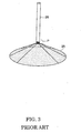
- the conventional discone antenna comprises a conical conductor element 21, and a disc-shaped conductor element 22 which is located closely to the conical conductor element 21 with a predetermined space being kept between a top of the conical conductor element 21 and the disc-shaped conductor element 22.
- the disc-shaped conductor element 22 is located coaxially with the conical conductor element 21. Namely, a rotation axis of the disc-shaped conductor element 22 is corresponding with that of the conical conductor element 21.
- a signal is supplied to the conventional discone antenna from a center of the disc-shaped conductor element 22 as a feeding point P while a ground voltage is supplied to the conventional discone antenna from a top of the conical conductor element 21 as a feeding point P.
- the conventional biconical antenna comprises two conical conductor elements 23 and 24.
- the two conical conductor elements 23 and 24 are located closely to each other with respective rotation central axes thereof being corresponding with each other and with respective tops thereof facing oppositely to each other.
- signals are supplied to the conventional biconical antenna from the respective tops of the two conical conductor elements 23 and 24 as respective feeding points P.
- the conventional Brown antenna comprises a conical conductor element 25, and a pole-shaped conductor element 26 which is located closely to the conical conductor element 25 with a predetermined space being kept between a top of the conical conductor element 25 and coaxially with the conical conductor element 25. Namely, a rotation axis of the pole-shaped conductor element 26 is corresponding with that of the conical conductor element 25.
- a signal is supplied to the conventional Brown antenna from an end of the pole-shaped conductor element 26 as a feeding point P while a ground voltage is supplied to the conventional Brown antenna from a top of the conical conductor element 25 as a feeding point P.
- Figs. 4 and 5 show an example of a structure of the antenna element in an actual product level.
- Fig. 4 shows an example of a structure of a conventional discone antenna
- Fig. 5 shows another example of a structure of a conventional discone antenna.
- the conventional discone antenna has a conical conductor element 21 and a disc-shaped conductor element 22.
- the disc-shaped conductor element 22 is similar to that illustrated in Fig. 1.
- a disc-shaped conductor element 22 in Fig. 5 comprises a linear annulus conductor portion 22a and a plurality of linear and radial conductor portions 22b which are located at pitches equal to each other and by which a center point of the linear and radial conductor portions 22b is connected to the linear annulus conductor portion 22a.
- the antenna element is composed of linear members thus mentioned. Namely, in order to obtain a desirable antenna shape or constitution, it becomes necessary that the linear members are fixed and holded by the use of an additional member of a separator, or the like made of insulating materials, such as a fluoride resin, an ABS resin, and the like. As a result, the structure of the antenna element inevitably becomes complicated. Accordingly, many manufacturing steps are required for mounting the antenna elements.
- Fig. 6 shows the antenna device according to the first embodiment of the present invention with a part of the antenna device being torn.
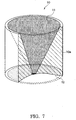
- Fig. 7 shows an antenna device according to a second embodiment of the present invention with a part of the antenna device being torn.
- Fig. 8 shows an antenna device according to a third embodiment of the present invention with a part of the antenna device being torn.
- Fig. 9 shows an antenna device according to a fourth embodiment of the present invention with a part of the antenna device being torn.
- Fig. 10 shows an antenna device according to a fifth embodiment of the present invention.
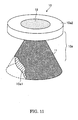
- Fig. 11 shows an antenna device according to a sixth embodiment of the present invention with a part of the antenna device being torn.
- Fig. 12 shows an antenna device according to a seventh embodiment of the present invention with a part of the antenna device being torn.
- the antenna device 10 forms a discone antenna and comprises a pole-shaped base member 10a which is composed of dielectric material.
- the pole-shaped base member 10a has a cone-shaped inner space formed therein.
- a first antenna element 11 is formed by patterning a metal conductor layer.
- a second antenna element 12 is formed also by circularly patterning a metal conductor layer at the side of a top of the first antenna element 11 with a predetermined space being kept between the top of the first antenna element 11 and the second antenna element 12.
- the first antenna element 11 and the second antenna element 12 are located with respective rotation central axes thereof being corresponding with each other.
- the pole-shaped base member 10a is composed, for example, ceramics (cordierite, forsterite, alumina, glassed ceramics, titanium oxide ceramics, and the like, or mixture of these materials), resin (polytetrafluoroethylene, polyimide, bismareimide, triazine, liquid crystal polymer, and the like), or a composite material of the ceramics and the resin can be used.
- ceramics cordierite, forsterite, alumina, glassed ceramics, titanium oxide ceramics, and the like, or mixture of these materials
- resin polytetrafluoroethylene, polyimide, bismareimide, triazine, liquid crystal polymer, and the like
- a composite material of the ceramics and the resin can be used.
- the antenna device 10 is mounted on a mounting surface of a substrate (not shown in Fig. 6) with the first antenna element 11 facing the mounting surface. Subsequently, by a coaxial cable 14 that is a feeding line, a signal is supplied to the antenna device 10 from a signal source (not shown in Fig. 6) with a center of the second antenna element 12 being a feeding point P while a ground voltage is supplied to the antenna device 10 from a top of the first antenna element 11 as a feeding point P.
- resonance can be obtained at a wide frequency band that ranges frequencies four times through eight times higher than the lowest frequency rendering an antenna to be resonated.
- Electrodes of which the first antenna element 11, the second antenna element 12, and the feeding point P are composed are formed by patterning a metal conductor layer, such as copper, silver, and the like.
- the electrodes are formed by a method that a metal paste, for example, of silver, and the like is burned onto the pole-shaped base member 10a by pattern printing, a method that a metal pattern layer is formed by plating, a method that a thin metal film is subjected to patterning by etching, a method that a metal member fabricated by plate work, or the like is fitted on the pole-shaped base member 10a, and so on.
- a signal is supplied to the first antenna element 11 by making the second antenna element 12 be at a ground voltage.
- a signal is supplied to the second antenna element 12 by making the first antenna element 11 be at a ground voltage. This will be applied similarly to the following embodiments.
- the coaxial cable 14 is omitted for the brevity of illustration. Further, it is not essential for the antenna device of the present invention to have a feeding line, such as a coaxial cable, and the like.
- the first antenna element 11 and the second antenna element 12 are formed integrally in the pole-shaped base member 10a composed of dielectric material.
- an antenna device having a desirable shape is assembled by the use of additional members each of a separator, or the like together with constitutional members each of an antenna element.
- the antenna device 10 can be obtained with a plain structure.
- the antenna device 10 is mounted on a substrate, as it stands.
- the first antenna element 11 is formed on inner surface of the pole-shaped base member 10a.
- the first antenna element 11 can be prevented from being injured when the antenna device 10 is handled or mounted on a substrate.
- FIG. 7 illustrated is the antenna device according to the second embodiment.
- the antenna device according to this embodiment is mounted on a substrate (not shown in Fig. 7) in the direction opposite to that of the first embodiment.
- the antenna device 10 according to this embodiment is mounted on the substrate with the second antenna element 12 facing a mounting surface of the substrate.
- a signal is supplied to the first antenna element 11 while a ground voltage is supplied to the second antenna element 12.
- the antenna device of the present invention is applied to an antenna other than the discone antenna, respectively.
- the antenna device 10 constitutes a biconical antenna.
- the antenna device 10 comprises a pole-shaped base member 10a, a first antenna element 11 and a second antenna element 12.
- Two conical inner spaces are formed in the pole-shaped base member 10a with respective rotation central axes thereof being corresponding with each other and with respective tops thereof facing oppositely to each other.
- the first antenna element 11 is formed in an inner surface of one of the two conical inner spaces while the second antenna element 12 is formed in an inner surface of another one of the two conical inner spaces.
- signals are supplied by the tops of the first antenna element 11 and the second antenna element 12 as a feeding point P.
- the antenna device 10 constitutes a Brown antenna.
- the antenna device 10 comprises a pole-shaped base member 10a, a first antenna element 11 and a second antenna element 12.
- a conical inner space is formed in the pole-shaped base member 10a.
- the first antenna element 11 is formed in the conical inner space.
- a thrender pole-shaped hole is formed in the pole-shaped base member 10a with a rotation axis of the thrender pole-shaped hole is corresponding with that of the first antenna element 11.
- the second antenna element 12 is formed in an inner surface of the thrender pole-shaped hole by patterning a metal conductor layer.
- a signal is supplied by the top of the first antenna element 11 and an end of the second antenna element 12 at the side of the first antenna element 11, namely, the end of the lower side in Fig. 9, as a feeding point P.
- the antenna device 10 forms a discone antenna and comprises a frustum circular cone-shaped base member 10a which is composed of dielectric material.
- the frustum circular cone-shaped base member 10a has a cone-shaped inner space formed therein.
- a first antenna element 11 is formed by patterning a metal conductor layer.
- a second antenna element 12 is formed also by circularly patterning a metal conductor layer at the side of a top of the first antenna element 11 with a predetermined space being kept between the top of the first antenna element 11 and the second antenna element 12.
- the first antenna element 11 and the second antenna element 12 are located with respective rotation central axes thereof being corresponding with each other.
- the frustum circular cone-shaped base member 10a is composed of a dielectric material similar to that of the first through the fourth embodiments.
- the antenna device 10 is mounted on a mounting surface of a substrate (not shown in Fig. 10) with the first antenna element 11 facing the mounting surface. Subsequently, by a coaxial cable (not shown) that is a feeding line, a signal is supplied to the antenna device 10 from a signal source (not shown in Fig. 10) with a center of the second antenna element 12 being a feeding point P while a ground voltage is supplied to the antenna device 10 from a top of the first antenna element 11 as a feeding point P.
- a coaxial cable not shown
- a signal is supplied to the antenna device 10 from a signal source (not shown in Fig. 10) with a center of the second antenna element 12 being a feeding point P while a ground voltage is supplied to the antenna device 10 from a top of the first antenna element 11 as a feeding point P.
- Electrodes of which the first antenna element 11, the second antenna element 12, and the feeding point P are composed are formed by patterning a metal conductor layer, similarly to the first through the fourth embodiments.
- a signal is supplied to the first antenna element 11 by making the second antenna element 12 be at a ground voltage.
- the first antenna element 11 and the second antenna element 12 are formed integrally in the frustum circular cone-shaped base member 10a composed of dielectric material.
- an antenna device having a desirable shape is assembled by the use of additional members each of a separator, or the like together with constitutional members each of an antenna element.
- the antenna device 10 can be obtained with a plain structure.
- the antenna device 10 is mounted on a substrate, as it stands.
- the first antenna element 11 is formed on inner surface of the frustum circular cone-shaped base member 10a.
- the first antenna element 11 can be prevented from being injured when the antenna device 10 is handled or mounted on a substrate.
- the antenna device 10 forms a discone antenna and comprises a frustum circular cone-shaped base member 10a which is composed of dielectric material.
- the frustum circular cone-shaped base member 10a is mainly consisting of two parts, one is a circular cone-shaped base member 10a1 and another is a circular plate-shaped base member 10a2.
- the circular cone-shaped base member 10a1 does not have a cone-shaped inner space formed therein, different from those of the first through the fifth embodiments.
- the whole of the circular cone-shaped base member 10a1 is filled with the dielectric material, as depicted by hatching lines in Fig. 11.
- the first antenna element 11 is formed on an outer surface of the circular cone-shaped base member 10a1.
- the circular plate-shaped base member 10a2 is filled with the dielectric material, similarly to the upper end portions of the pole-shaped base member 10a in the first embodiment.
- the second antenna element 12 is formed on a plain surface of the circular plate-shaped base member 10a2, similarly to that of the first embodiment.
- the antenna device 10 may form a biconical antenna and comprises two circular cone-shaped base members 10a1 each of which is filled with the dielectric material and has an outer surface.
- the two circular cone-shaped base members 10a1 are located with respective tops thereof facing oppositely to each other.
- a first antenna element may be formed on an outer surface of one of the two circular cone-shaped base members 10a1 while a second antenna element may be formed on an outer surface of another one of the two circular cone-shaped base members 10a1.
- the antenna device 10 forms a dipole antenna and comprises a circular tube-shaped base member 10a which is composed of dielectric material and which has a predetermined thickness between inner and outer surfaces thereof.
- the circular tube-shaped base member 10a has two inner spaces formed from both ends of the circular tube-shaped base member 10a.
- a cylindrical first antenna element 11 and a cylindrical second antenna element 12 are formed on the two inner spaces, respectively.
- the antenna device 10 Under the condition that the antenna device 10 is mounted in a wireless communication apparatus, by a coaxial cable 14, a signal and a ground voltage are supplied to the antenna device 10, respectively, with end surfaces of the cylindrical first antenna element 11 and the cylindrical second antenna element 12 being used as a feeding point P.
- the third parasitic antenna element 13 to which neither signals nor ground voltage are feeded is formed on the outer surface of the circular tube-shaped base member 10a with a distance corresponding to the predetermined thickness of the circular tube-shaped base member 10a being kept with respect to the first and the second antenna elements 11 and 12, as illustrated in Fig. 12.
- the third parasitic antenna element 13 is formed partially on the outer surface of the circular tube-shaped base member 10a to have a predetermined area on the outer surface, as depicted by the area having plenty of specks in Fig. 12.
- the third parasitic antenna element 13 is formed, as mentioned above, in the antenna device 10 according to this embodiment.
- the antenna device 10 can be tuned to have desirable antenna characteristics by adjusting the third parasitic antenna element 13, for example, by adjusting a size of the predetermined area of the third parasitic antenna element 13 on the outer surface of the circular tube-shaped base member 10a.
- the third parasitic antenna element 13 is formed on the outer surface of the circular tube-shaped base member 10a.
- the third parasitic antenna element 13 can be formed on an inner or a plain surface of the circular tube-shaped base member 10a.
- a configuration of the third parasitic antenna element 13 can be freely determined so that the antenna device 10 may have the above-mentioned desirable antenna characteristics.
- the first antenna element 11 and the second antenna element 12 are formed integrally in the base member 10a composed of dielectric material.
- the antenna device 10 can be obtained with a plain structure.
- the antenna device 10 is mounted on a substrate, as it stands.
- a pole-shaped base member 10a is used in the first through fourth embodiments, respectively while a frustum of circular cone-shaped base member 10a is used in the fifth embodiment.
- the base member 10a is not restricted to those configurations.
- the base member 10a may have a cylinder-shaped configuration, a pyramid-shaped configuration, a frustum of pyramid-shaped configuration, or the like.
- the first antenna element 11 has circular cone-shaped configurations, respectively in the first through fifth embodiments.
- the first antenna element 11 may have various three-dimensional configurations, such as a pyramid-shaped configuration, a pole-shaped (a circular pole-shaped, a triangular prism pole-shaped, a rectangular prism pole-shaped, and the like) configuration, a tube-shaped (a circular tube-shaped, a triangular prism tube-shaped, a rectangular prism tube-shaped, and the like) configuration, a helicoid-shaped configuration, or the like.
- the first antenna element 11 is formed to have those three-dimensional configurations, it is not necessary that the first antenna element 11 is formed on a whole of the peripheral surface of the base member 10a in the peripheral direction.
- the second antenna element 12 has circular configurations, respectively in the first through third, and the fifth embodiments while the second antenna element 12 has the circular pole-shaped configuration in the fourth embodiment.
- the second antenna element 12 is not restricted to those configurations. Namely, as far as the second antenna element 12 is formed to have those plane-shaped configurations, the second antenna element 12 may have various two-dimensional configurations, such as square, rectangular, circular, elliptical configurations, and any configurations other than these.
- configurations of the first and the second antenna elements 11 and 12 thus mentioned can be formed by patterning a metal conductor layer on a whole area in line with respective configurations in the first through fifth embodiments.
- the configurations of the first and the second antenna elements 11 and 12 may be formed in another manner.
- many linear metal conductor layers may be formed radially from a certain point so as to constitute, as a whole, a circular configuration, a circular cone-shaped configuration, or the like.
- metal conductor layers may be formed with a mesh structure so as to constitute; as a whole, a desirable configuration.
- the antenna device of the present invention can be used in various wireless communication apparatus, such as, a portable telephone, a mobile terminal, an included antenna of an wireless LAN card, and the like.
Landscapes
- Engineering & Computer Science (AREA)
- Computer Networks & Wireless Communication (AREA)
- Details Of Aerials (AREA)
Applications Claiming Priority (2)
| Application Number | Priority Date | Filing Date | Title |
|---|---|---|---|
| JP2003023550A JP3746487B2 (ja) | 2003-01-31 | 2003-01-31 | アンテナ装置およびそれを用いた無線通信装置 |
| JP2003023550 | 2003-01-31 |
Publications (2)
| Publication Number | Publication Date |
|---|---|
| EP1443597A1 true EP1443597A1 (de) | 2004-08-04 |
| EP1443597B1 EP1443597B1 (de) | 2008-01-16 |
Family
ID=32652912
Family Applications (1)
| Application Number | Title | Priority Date | Filing Date |
|---|---|---|---|
| EP04002170A Expired - Lifetime EP1443597B1 (de) | 2003-01-31 | 2004-01-30 | Antenne und Funkgerät mit einer derartigen Antenne |
Country Status (4)
| Country | Link |
|---|---|
| US (1) | US6972726B2 (de) |
| EP (1) | EP1443597B1 (de) |
| JP (1) | JP3746487B2 (de) |
| DE (1) | DE602004011276T2 (de) |
Families Citing this family (16)
| Publication number | Priority date | Publication date | Assignee | Title |
|---|---|---|---|---|
| JP4551151B2 (ja) * | 2004-07-27 | 2010-09-22 | 株式会社日本ジー・アイ・ティー | バイコニカル・アンテナ |
| US7221326B2 (en) * | 2004-07-27 | 2007-05-22 | Git Japan, Inc. | Biconical antenna |
| JP3741139B1 (ja) * | 2004-08-26 | 2006-02-01 | オムロン株式会社 | 無線機器 |
| US20070241982A1 (en) * | 2004-09-30 | 2007-10-18 | Alan Stigliani | Contoured triangular dipole antenna |
| US7245263B2 (en) * | 2005-02-18 | 2007-07-17 | Ricoh Company, Ltd. | Antenna |
| US8264417B2 (en) * | 2007-06-19 | 2012-09-11 | The United States Of America As Represented By The Secretary Of The Navy | Aperture antenna with shaped dielectric loading |
| US7940225B1 (en) | 2007-06-19 | 2011-05-10 | The United States Of America As Represented By The Secretary Of The Navy | Antenna with shaped dielectric loading |
| US8395559B1 (en) * | 2010-09-13 | 2013-03-12 | The United States Of America As Represented By The Secretary Of The Navy | Capacitive loaded grid antenna |
| US8576135B1 (en) * | 2011-01-28 | 2013-11-05 | Olympus Corporation | Bicone antenna |
| US9521766B2 (en) * | 2012-06-27 | 2016-12-13 | CommScope Connectivity Belgium BVBA | High density telecommunications systems with cable management and heat dissipation features |
| US9768520B2 (en) * | 2013-08-09 | 2017-09-19 | Harris Corporation | Broadband dual polarization omni-directional antenna and associated methods |
| US9692136B2 (en) * | 2014-04-28 | 2017-06-27 | Te Connectivity Corporation | Monocone antenna |
| CN106876866B (zh) * | 2017-03-15 | 2023-09-29 | 浙江悦和科技有限公司 | 具有rfid标签的绝缘堵头 |
| US11223114B2 (en) * | 2019-12-27 | 2022-01-11 | Harman International Industries, Incorporated | Antenna system for a vehicle telematics unit |
| RU2739868C1 (ru) * | 2020-05-18 | 2020-12-29 | Российская Федерация, от имени которой выступает Государственная корпорация по атомной энергии "Росатом" (Госкорпорация "Росатом") | Кольцевая щелевая антенна |
| US11862854B1 (en) * | 2023-05-12 | 2024-01-02 | The Florida International University Board Of Trustees | Dual-band antenna arrays and methods of fabricating the same |
Citations (4)
| Publication number | Priority date | Publication date | Assignee | Title |
|---|---|---|---|---|
| US3868694A (en) * | 1973-08-09 | 1975-02-25 | Us Air Force | Dielectric directional antenna |
| JPH0983238A (ja) * | 1995-09-18 | 1997-03-28 | Harada Ind Co Ltd | 多波共用アンテナ装置 |
| US6052889A (en) * | 1996-11-21 | 2000-04-25 | Raytheon Company | Radio frequency antenna and its fabrication |
| EP1189305A2 (de) * | 2000-09-13 | 2002-03-20 | ZENDAR S.p.A. | Kurze, drahtlose Antenne |
Family Cites Families (4)
| Publication number | Priority date | Publication date | Assignee | Title |
|---|---|---|---|---|
| FR2246090B1 (de) * | 1973-08-31 | 1977-05-13 | Thomson Csf | |
| JPH08139515A (ja) | 1994-11-11 | 1996-05-31 | Toko Inc | 誘電体垂直偏波アンテナ |
| JP3515459B2 (ja) | 1999-12-22 | 2004-04-05 | 三菱電機株式会社 | 無指向性アンテナ |
| JP4722254B2 (ja) | 2000-05-01 | 2011-07-13 | 亮 伊藤 | 筒体内面ヘリカルアンテナ |
-
2003
- 2003-01-31 JP JP2003023550A patent/JP3746487B2/ja not_active Expired - Fee Related
-
2004
- 2004-01-29 US US10/765,957 patent/US6972726B2/en not_active Expired - Fee Related
- 2004-01-30 DE DE602004011276T patent/DE602004011276T2/de not_active Expired - Fee Related
- 2004-01-30 EP EP04002170A patent/EP1443597B1/de not_active Expired - Lifetime
Patent Citations (4)
| Publication number | Priority date | Publication date | Assignee | Title |
|---|---|---|---|---|
| US3868694A (en) * | 1973-08-09 | 1975-02-25 | Us Air Force | Dielectric directional antenna |
| JPH0983238A (ja) * | 1995-09-18 | 1997-03-28 | Harada Ind Co Ltd | 多波共用アンテナ装置 |
| US6052889A (en) * | 1996-11-21 | 2000-04-25 | Raytheon Company | Radio frequency antenna and its fabrication |
| EP1189305A2 (de) * | 2000-09-13 | 2002-03-20 | ZENDAR S.p.A. | Kurze, drahtlose Antenne |
Non-Patent Citations (1)
| Title |
|---|
| PATENT ABSTRACTS OF JAPAN vol. 1997, no. 07 31 July 1997 (1997-07-31) * |
Also Published As
| Publication number | Publication date |
|---|---|
| JP2004236086A (ja) | 2004-08-19 |
| US6972726B2 (en) | 2005-12-06 |
| DE602004011276D1 (de) | 2008-03-06 |
| DE602004011276T2 (de) | 2009-01-15 |
| EP1443597B1 (de) | 2008-01-16 |
| US20040183736A1 (en) | 2004-09-23 |
| JP3746487B2 (ja) | 2006-02-15 |
Similar Documents
| Publication | Publication Date | Title |
|---|---|---|
| US6972726B2 (en) | Antenna device and wireless communication apparatus using the same | |
| EP3571743B1 (de) | Antennen mit verbessertem empfang von satellitensignalen | |
| EP2297817B1 (de) | Geklappte konische antenne und diesbezügliche verfahren | |
| US6842148B2 (en) | Fabrication method and apparatus for antenna structures in wireless communications devices | |
| EP3930098B1 (de) | Zirkular polarisierte antennen mit verbundenem schlitz | |
| EP3241257B1 (de) | Zirkularpolarisierte angeschlossene schlitzantenne | |
| US8405552B2 (en) | Multi-resonant broadband antenna | |
| US20020109642A1 (en) | Tuning circuit for edge-loaded nested resonant radiators that provides switching among several wide frequency bands | |
| EP1396049B1 (de) | Zweiband-dipolantennenstruktur | |
| JP2004304785A (ja) | 指向性可変アンテナおよび該アンテナを用いた電子機器、ならびに該アンテナを用いたアンテナ指向性制御方法 | |
| US7626555B2 (en) | Antenna arrangement and method for making the same | |
| KR20050058229A (ko) | 초광대역 어플리케이션용 3차원 전방향성 안테나 설계 | |
| KR20110018920A (ko) | 광대역 터미네이티드 디스콘 안테나 및 관련된 방법 | |
| JP2003188642A (ja) | 多周波帯域アンテナ | |
| JP2761195B2 (ja) | 環状マイクロストリップアンテナ素子及びラジアルラインアンテナ装置 | |
| US7245263B2 (en) | Antenna | |
| EP1756908B1 (de) | Verfahren und einrichtung zum speisen von planarantennen | |
| WO2000026990A1 (en) | Helical antenna | |
| JPH09232857A (ja) | マイクロストリップアンテナ | |
| CN107078393B (zh) | 无线电子设备 | |
| US10944163B2 (en) | Bung-type antenna and antennal structure and antennal assembly associated therewith | |
| JP4475583B2 (ja) | ディスコーンアンテナおよび該ディスコーンアンテナを用いた情報通信機器 | |
| US12027765B2 (en) | Corrugated ground plane apparatus for an antenna | |
| JP6519526B2 (ja) | アンテナ装置 | |
| JP2005217897A (ja) | アンテナ装置 |
Legal Events
| Date | Code | Title | Description |
|---|---|---|---|
| PUAI | Public reference made under article 153(3) epc to a published international application that has entered the european phase |
Free format text: ORIGINAL CODE: 0009012 |
|
| AK | Designated contracting states |
Kind code of ref document: A1 Designated state(s): AT BE BG CH CY CZ DE DK EE ES FI FR GB GR HU IE IT LI LU MC NL PT RO SE SI SK TR |
|
| AX | Request for extension of the european patent |
Extension state: AL LT LV MK |
|
| 17P | Request for examination filed |
Effective date: 20040830 |
|
| 17Q | First examination report despatched |
Effective date: 20050223 |
|
| AKX | Designation fees paid |
Designated state(s): DE FR GB NL |
|
| RBV | Designated contracting states (corrected) |
Designated state(s): DE FR GB NL |
|
| 17Q | First examination report despatched |
Effective date: 20050223 |
|
| 17Q | First examination report despatched |
Effective date: 20050223 |
|
| GRAP | Despatch of communication of intention to grant a patent |
Free format text: ORIGINAL CODE: EPIDOSNIGR1 |
|
| GRAS | Grant fee paid |
Free format text: ORIGINAL CODE: EPIDOSNIGR3 |
|
| GRAA | (expected) grant |
Free format text: ORIGINAL CODE: 0009210 |
|
| AK | Designated contracting states |
Kind code of ref document: B1 Designated state(s): DE FR GB NL |
|
| REG | Reference to a national code |
Ref country code: GB Ref legal event code: FG4D |
|
| REF | Corresponds to: |
Ref document number: 602004011276 Country of ref document: DE Date of ref document: 20080306 Kind code of ref document: P |
|
| PGFP | Annual fee paid to national office [announced via postgrant information from national office to epo] |
Ref country code: NL Payment date: 20080130 Year of fee payment: 5 Ref country code: GB Payment date: 20080303 Year of fee payment: 5 Ref country code: DE Payment date: 20080131 Year of fee payment: 5 |
|
| PGFP | Annual fee paid to national office [announced via postgrant information from national office to epo] |
Ref country code: FR Payment date: 20080129 Year of fee payment: 5 |
|
| ET | Fr: translation filed | ||
| PLBE | No opposition filed within time limit |
Free format text: ORIGINAL CODE: 0009261 |
|
| STAA | Information on the status of an ep patent application or granted ep patent |
Free format text: STATUS: NO OPPOSITION FILED WITHIN TIME LIMIT |
|
| 26N | No opposition filed |
Effective date: 20081017 |
|
| GBPC | Gb: european patent ceased through non-payment of renewal fee |
Effective date: 20090130 |
|
| NLV4 | Nl: lapsed or anulled due to non-payment of the annual fee |
Effective date: 20090801 |
|
| PG25 | Lapsed in a contracting state [announced via postgrant information from national office to epo] |
Ref country code: DE Free format text: LAPSE BECAUSE OF NON-PAYMENT OF DUE FEES Effective date: 20090801 |
|
| REG | Reference to a national code |
Ref country code: FR Ref legal event code: ST Effective date: 20091030 |
|
| PG25 | Lapsed in a contracting state [announced via postgrant information from national office to epo] |
Ref country code: NL Free format text: LAPSE BECAUSE OF NON-PAYMENT OF DUE FEES Effective date: 20090801 Ref country code: GB Free format text: LAPSE BECAUSE OF NON-PAYMENT OF DUE FEES Effective date: 20090130 |
|
| PG25 | Lapsed in a contracting state [announced via postgrant information from national office to epo] |
Ref country code: FR Free format text: LAPSE BECAUSE OF NON-PAYMENT OF DUE FEES Effective date: 20090202 |