EP1443563A2 - Light emitting display panel and method of manufacturing the same - Google Patents
Light emitting display panel and method of manufacturing the same Download PDFInfo
- Publication number
- EP1443563A2 EP1443563A2 EP04001889A EP04001889A EP1443563A2 EP 1443563 A2 EP1443563 A2 EP 1443563A2 EP 04001889 A EP04001889 A EP 04001889A EP 04001889 A EP04001889 A EP 04001889A EP 1443563 A2 EP1443563 A2 EP 1443563A2
- Authority
- EP
- European Patent Office
- Prior art keywords
- transparent substrate
- microlens array
- light emitting
- resin
- light
- Prior art date
- Legal status (The legal status is an assumption and is not a legal conclusion. Google has not performed a legal analysis and makes no representation as to the accuracy of the status listed.)
- Withdrawn
Links
Images



Classifications
-
- H—ELECTRICITY
- H10—SEMICONDUCTOR DEVICES; ELECTRIC SOLID-STATE DEVICES NOT OTHERWISE PROVIDED FOR
- H10K—ORGANIC ELECTRIC SOLID-STATE DEVICES
- H10K59/00—Integrated devices, or assemblies of multiple devices, comprising at least one organic light-emitting element covered by group H10K50/00
- H10K59/80—Constructional details
- H10K59/87—Passivation; Containers; Encapsulations
- H10K59/871—Self-supporting sealing arrangements
- H10K59/8722—Peripheral sealing arrangements, e.g. adhesives, sealants
-
- B—PERFORMING OPERATIONS; TRANSPORTING
- B26—HAND CUTTING TOOLS; CUTTING; SEVERING
- B26F—PERFORATING; PUNCHING; CUTTING-OUT; STAMPING-OUT; SEVERING BY MEANS OTHER THAN CUTTING
- B26F1/00—Perforating; Punching; Cutting-out; Stamping-out; Apparatus therefor
- B26F1/32—Hand-held perforating or punching apparatus, e.g. awls
-
- B—PERFORMING OPERATIONS; TRANSPORTING
- B26—HAND CUTTING TOOLS; CUTTING; SEVERING
- B26D—CUTTING; DETAILS COMMON TO MACHINES FOR PERFORATING, PUNCHING, CUTTING-OUT, STAMPING-OUT OR SEVERING
- B26D7/00—Details of apparatus for cutting, cutting-out, stamping-out, punching, perforating, or severing by means other than cutting
- B26D7/01—Means for holding or positioning work
- B26D7/02—Means for holding or positioning work with clamping means
-
- H—ELECTRICITY
- H10—SEMICONDUCTOR DEVICES; ELECTRIC SOLID-STATE DEVICES NOT OTHERWISE PROVIDED FOR
- H10K—ORGANIC ELECTRIC SOLID-STATE DEVICES
- H10K50/00—Organic light-emitting devices
- H10K50/80—Constructional details
- H10K50/85—Arrangements for extracting light from the devices
- H10K50/858—Arrangements for extracting light from the devices comprising refractive means, e.g. lenses
-
- H—ELECTRICITY
- H10—SEMICONDUCTOR DEVICES; ELECTRIC SOLID-STATE DEVICES NOT OTHERWISE PROVIDED FOR
- H10K—ORGANIC ELECTRIC SOLID-STATE DEVICES
- H10K59/00—Integrated devices, or assemblies of multiple devices, comprising at least one organic light-emitting element covered by group H10K50/00
- H10K59/80—Constructional details
- H10K59/875—Arrangements for extracting light from the devices
- H10K59/879—Arrangements for extracting light from the devices comprising refractive means, e.g. lenses
-
- B—PERFORMING OPERATIONS; TRANSPORTING
- B26—HAND CUTTING TOOLS; CUTTING; SEVERING
- B26D—CUTTING; DETAILS COMMON TO MACHINES FOR PERFORATING, PUNCHING, CUTTING-OUT, STAMPING-OUT OR SEVERING
- B26D7/00—Details of apparatus for cutting, cutting-out, stamping-out, punching, perforating, or severing by means other than cutting
- B26D7/01—Means for holding or positioning work
- B26D2007/013—Means for holding or positioning work the work being tubes, rods or logs
-
- H—ELECTRICITY
- H10—SEMICONDUCTOR DEVICES; ELECTRIC SOLID-STATE DEVICES NOT OTHERWISE PROVIDED FOR
- H10K—ORGANIC ELECTRIC SOLID-STATE DEVICES
- H10K59/00—Integrated devices, or assemblies of multiple devices, comprising at least one organic light-emitting element covered by group H10K50/00
-
- H—ELECTRICITY
- H10—SEMICONDUCTOR DEVICES; ELECTRIC SOLID-STATE DEVICES NOT OTHERWISE PROVIDED FOR
- H10K—ORGANIC ELECTRIC SOLID-STATE DEVICES
- H10K59/00—Integrated devices, or assemblies of multiple devices, comprising at least one organic light-emitting element covered by group H10K50/00
- H10K59/80—Constructional details
- H10K59/8791—Arrangements for improving contrast, e.g. preventing reflection of ambient light
Definitions
- the present invention relates to a light emitting display panel using a light emitting element such as an organic electroluminescent element (hereinafter referred to as an organic EL element) and a manufacturing method of the light emitting display panel.
- a light emitting element such as an organic electroluminescent element (hereinafter referred to as an organic EL element)
- an organic EL element organic electroluminescent element
- a light emitting layer (a plurality of light emitting elements) having a plurality of transparent electrodes parallel to each other, an organic EL material layer, and a metal electrode stacked in this order, is formed on a transparent substrate. Further, terminal lines extended from the transparent electrodes and the metal electrode are formed to connect a drive circuit.
- the light emitting layer is held in a sealed environment provided by adhering a sealing case to the transparent substrate via an adhesive, thus preventing deterioration of the light emitting efficiency that might otherwise be caused by atmospheric moisture (see for example JP 2000-243556 A, page 3, FIG. 1)
- the conventional light emitting display panel as described above has a structure in which the light emitting elements are disposed on one surface of the transparent substrate and display light is emitted from the other surface of the transparent substrate.
- the refractive index of the transparent substrate made of glass typically 1.50 in case of glass
- the atmosphere air, typically 1.00
- total reflection occurs at the boundary face between the transparent substrate and the atmosphere on the emitted light that makes a larger angle with the normal to the surface of the transparent substrate than the critical angle.
- This causes a problem of lower light-extraction efficiency because such light is diffused in the transparent substrate or disappears by attenuation through the transparent substrate.
- the present invention is intended to cope with the problems described above. Therefore, one object of the present invention is to provide a light emitting display panel that has a higher light-extraction efficiency than prior art panels, prevents reflection of incident light from outside, and has an improved appearance of the display, an improved current efficiency, and an extended life time of the panel. Another object of the invention is to provide a method of manufacturing such light emitting display panel.
- the claimed structure light from the light emitting elements is hardly reflected by a boundary face between the transparent substrate and the atmosphere and also the incident light from outside can be diffusely reflected.
- the light-extraction efficiency can be improved resulting in an improvement of the light-emission efficiency, and, furthermore, the display can be easily recognized because reflection of the incident light is prevented.
- the microlens array can be adhered to the second surface of the transparent substrate via an adhesive. According to this structure, concavity and convexity can be easily formed on the display face of the transparent substrate.
- the microlens array can be disposed on a first surface of a substrate made of the same material as the transparent substrate, and a second surface of the substrate can be adhered to the second surface of the transparent substrate via adhesive.
- the microlens array can be formed on a flat surface, microfabrication technologies can be utilized to form a very fine microlens array.
- the reflection of the incident light can be prevented to provide clearer image display in a bright condition, and also the microlens can be manufactured with fewer manufacturing steps, which can reduce a manufacturing cost of the light emitting display panel.
- the microlens array can be made of a transparent material having a refractive index substantially equal to or higher than that of the transparent substrate. According to this structure, since, from a view point of a refractive index, the microlens array is not less than the transparent substrate, the light from the light emitting elements is output with little reflection by the boundary face between the transparent substrate and the microlens array. Moreover, the incident light from the transparent substrate side to the microlens array side with a large incident angle is output with a smaller angle than the incident angle. In other words, since the angle of a large part of the output light can be reduced to be smaller than the critical angle, only little light is reflected by the total reflection phenomenon. Thus the light-extraction efficiency can be improved resulting in improvement of the light-emission efficiency. Moreover, since the power consumption necessary for light emission can be reduced, life of the light emitting elements can be extended.
- the adhesive can be made of a transparent material having a refractive index that is substantially equal to or higher than that of the transparent substrate and substantially equal to or lower than that of the microlens array. According to this structure, since, from a view point of a refractive index, the microlens array is not less than the adhesive and the adhesive is not less than the transparent substrate, the light from the light emitting elements is output with little reflection caused by the total reflection at the boundary faces between the transparent substrate and the adhesive and between the adhesive and the microlens array, thus enhancing the light-extraction efficiency.
- the adhesive can be made of a material that cures at a temperature lower than that of a glass transition point of a material forming the light emitting element. According to this structure, it can be prevented that the heat-sensitive light emitting elements are damaged by heat applied to cure the adhesive when adhering the microlens array with the transparent substrate.
- the adhesive can be made of a material cured by visible radiation. According to this structure, it can be prevented that the light emitting elements sensitive to heat and ultraviolet lays are damaged by ultraviolet lays irradiated to cure the adhesive when adhering the microlens array with the transparent substrate.
- the microlens array can comprise a plurality of convex microlenses sized within a range of 1 through 100 micrometer. According to this structure, a high efficiency of reducing the incident light reflection can be obtained, and thus enhancing the light-extraction efficiency of the light emitting elements.
- the light emitting element can be formed by sequentially stacking at least a transparent electrode, a light emitting layer, and a metal electrode above the first surface of the transparent substrate in this order.
- the light emitting layer can comprise a layer of an organic EL material.
- an antireflective agent is applied on at least the second surface of the transparent substrate and the surface of the microlens array. According to this structure, reflection of the light emitted from the light emitting elements caused by the total reflection phenomenon and reflection of the incident light from outside can be reduced, thus enhancing the light-extraction efficiency. Accordingly the light-emission efficiency can be improved, and the display appearance of the light emitting display panel can also be improved.
- the microlens array can be easily formed of thermosetting resin. Thus the cost of the light emitting display panel can be reduced.
- the microlens array since a hard substrate is directly processed to form the microlens array, the microlens array is durable against wear even if it is exposed to outside. Thus a light emitting display panel having a durable surface can be provided.
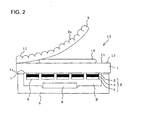
- FIG. 1 illustrates the structure of a first embodiment of the present invention.
- the reference numeral 1 denotes a transparent substrate.
- a plurality of light emitting elements (organic EL elements) 5 are disposed on a first surface 1a (the lower surface in Fig. 1) of the transparent substrate 1.
- Each of the light emitting elements 5 is formed by sequentially stacking a transparent electrode 2 made of indium tin oxide (hereinafter referred to as ITO) or the like, an organic EL material layer 3 formed of a light emitting functional layer or multiple layers including at least the light emitting functional layer, and a metal electrode 4.
- ITO indium tin oxide
- a sealing member 6 made of, for example, glass is disposed on the first surface 1a of the transparent substrate 1 via an adhesive 7 to seal the surrounding area of the light emitting elements.
- the sealing member 6 prevents the light emission property of the light emitting elements 5 from deteriorating with moisture.
- a desiccating agent 8 is disposed on an inner surface of the sealing member 6 within a space X formed between the sealing member 6 and the transparent substrate 1 for drying the space X to prevent the light emission property of the light emitting elements 5 from deteriorating with moisture.
- the adhesive 10 is made of transparent thermosetting resin whose refractive index is substantially equal to or lower than that of the microlens array 9 and substantially equal to or higher than that of the transparent substrate 1.
- the thermosetting resin that cures at a temperature lower than the lowest one of glass transition points (Tg points) of organic materials forming the light emitting element 5 is recommended. More preferably, the thermosetting resin should cure at a temperature of 10 or more degrees centigrade lower than the lowest Tg point. This is because the light emitting elements 5 that are sensitive to heat should be prevented from being damaged when the microlens array 9 is adhered to the transparent substrate 1.
- a thermosetting resin that cures with visible light radiation is also preferable.
- an antireflection (AR) coating 11 is applied to the surfaces of the microlens array 9 and the transparent substrate 1 to prevent reflection of light emitted from the light emitting elements 5 and reflection of incident light from outside.
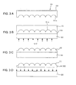
- a method of manufacturing the microlens array 9 is explained hereinafter with reference to the process chart shown in FIG. 3.
- the microlens array 9 thus manufactured is adhered to the second surface 1b (the upper surface) of the transparent substrate 1 via the adhesive 10 as shown in FIG. 2, the transparent substrate 1 having the plurality of light emitting elements 5 on the first surface 1a (the lower surface) thereof sealed with the sealing member 6.
- This assembly together with a circuit board not shown in the drawings having a drive circuit for driving the light emitting elements 5, forms the light emitting display panel 12.
- one or more desired ones of the light emitting elements 5 emit light under the control of the drive circuit in the circuit board, and the light is emitted to the outside via the transparent substrate 1 and the microlens array 9.
- the refractive index of the adhesive 10 is smaller than that of the microlens array 9 and the refractive index of the transparent substrate 1 is smaller than that of the adhesive 10, the light from the light emitting elements 5 can be emitted without being reflected at any boundary surfaces between the transparent substrate 1 and the adhesive 10 or between the adhesive 10 and the microlens array 9.
- the refractive index of the microlens array 9 is higher than those of the transparent substrate 1 and the adhesive 10, light incident from the transparent substrate side to the microlens array side with a large incident angle is output with a smaller angle than the incident angle.
- the angle of a large part of the output light can be reduced to be smaller than the critical angle, only little light is reflected by the total reflection phenomenon.
- the extraction efficiency of the light from the light emitting elements 5 can be improved resulting in an improvement of the light-emission efficiency.
- the life time of the light emitting elements 5 can be extended.
- the refractive index of the microlens array 9 is higher than that of room air, the light from the microlens array side could be reflected by the boundary face between the microlens array 9 and the room air.
- the surface of the microlens array 9 is made uneven by the convex lenses 9a, the light can hardly be reflected but rather be emitted. Further, incident light from outside can also be reflected diffusely by the uneven surface of the microlens array 9.
- the light-extraction efficiency can be improved resulting in an improvement of the light-emission efficiency, and it is also possible to make the display to be easily recognized by preventing reflection of the incident light.
- the surfaces of the transparent substrate 1 and the microlens array 9 are coated with the AR coating 11, the reflection of the light emitted by the light emitting elements 5 and also the incident light from outside can be even further prevented. Accordingly the light-emission efficiency can be improved, and the display appearance of the light emitting display panel 12 can also be improved.
- the microlens array 9 is made of thermosetting resin that is easy to be molded, the cost of the light emitting display panel 12 can be reduced.
- the light emitting display panel 12 as described above is suitable for articles that are expected to be used in bright places or mobile equipments that require low power consumption, such as a cellular phone, a personal digital assistant (PDA), or an in-vehicle TV.
- a cellular phone such as a cellular phone, a personal digital assistant (PDA), or an in-vehicle TV.
- PDA personal digital assistant
- FIG. 4 illustrates the structure of a second embodiment of the present invention.
- the light emitting display panel 12 of the first embodiment further comprises a substrate 13 which, instead of the microlens array 9, is adhered to the second surface 1b (the upper surface in the figure) of the transparent substrate 1 via the adhesive 10, the substrate 13 being made of the same material, e.g. glass, as the transparent substrate 1 and having the microlens array 9 disposed on one surface thereof (the upper surface in the figure).
- a method of manufacturing the microlens array 9 is explained hereinafter with reference to the process chart shown in FIG. 5.
- FIG. 4 An assembly of the microlens array 9 and the substrate 13 thus manufactured is, as shown in FIG. 4, adhered to the second surface 1b (the upper surface in the figure) of the transparent substrate 1 via the adhesive 10 so that the microlens array 9 side is positioned on the upper side, the transparent substrate 1 having the plurality of light emitting elements 5 on its first surface 1a (the lower surface in the figure) sealed with the sealing member 6.
- This assembly together with a circuit board not shown in the drawings having a drive circuit for driving the light emitting elements 5, forms the light emitting display panel 12.
- microlens array 9 can be formed on a flat surface of the substrate 13, microfabrication technologies can be utilized to make the microlens array 9 very fine. Thus the reflection of the incident light can be prevented to provide clearer image display in a bright surrounding. Also, the microlens can be manufactured with fewer manufacturing steps, which can reduce the manufacturing cost of the light emitting display panel 12.
- the third embodiment corresponds to the second embodiment with the difference that the substrate 13 to which the microlens array 9 is adhered, is replaced by a substrate 14 on which the microlens array 9 is formed by processing the substrate 14 itself.
- a method of manufacturing the microlens array 9 is explained hereinafter with reference to the process chart shown in FIG. 6.
- the microlens array 9 thus formed by directly processing the substrate 14 is adhered to the second surface 1b of the transparent substrate 1 via the adhesive 10 so that the microlens array side is positioned on the upper side, the transparent substrate 1 having the plurality of light emitting elements 5 on its first surface 1a sealed with the sealing member 6.
- This assembly together with a circuit board not shown in the drawings having a drive circuit for driving the light emitting elements 5, forms the light emitting display panel 12. Note that this assembly is not shown in any of the drawings but corresponds to that shown in Fig. 4 if the reference numeral 14 is substituted for 13 in Fig. 4.
- the microlens array 9 itself is made of glass that is hard, the microlens array 9 is durable against wear even if it is exposed to the outside. Thus a light emitting display panel 12 having a surface durable against scratches and difficult to be damaged can be provided.
Landscapes
- Life Sciences & Earth Sciences (AREA)
- Forests & Forestry (AREA)
- Engineering & Computer Science (AREA)
- Mechanical Engineering (AREA)
- Physics & Mathematics (AREA)
- Optics & Photonics (AREA)
- Electroluminescent Light Sources (AREA)
- Devices For Indicating Variable Information By Combining Individual Elements (AREA)
Abstract
Description
- FIG. 1
- schematically illustrates the structure of a first embodiment of the present invention;
- FIG. 2
- illustrates how the microlens array is applied to the substrate in the first embodiment;
- FIG. 3
- illustrates steps of a manufacturing process of a microlens array according to the first embodiment;
- FIG. 4
- schematically illustrates the structure of a second embodiment of the present invention;
- FIG. 5
- illustrates steps of a manufacturing process of a microlens array according to the second embodiment; and
- FIG.6
- illustrates steps of a manufacturing process of a microlens array according to a third embodiment.
Claims (14)
- A light emitting display panel, comprising:a transparent substrate (1) equipped with one or more light emitting elements (5) on a first surface (1a) thereof, a second surface (1b) of the transparent substrate (1) defining a display surface; anda microlens array (9) disposed on or above the second surface (1b) of the transparent substrate (1).
- The panel according to Claim 1, wherein; the microlens array (9) is adhered to the second surface (1b) of the transparent substrate (1) by means of an adhesive (10).
- The panel according to Claim 1, wherein
the microlens array (9) is disposed on a first surface of a second substrate (13; 14) made of the same material as the transparent substrate (1); and
a second surface of the second substrate (13; 14) is adhered to the second surface (1 b) of the transparent substrate (1) by means of an adhesive (10). - The panel according to any one of Claims 1 through 3, wherein the microlens array (9) is made of a transparent material having a refraction index substantially equal to or higher than that of the transparent substrate (1).
- The panel according to any one of Claims 2 through 4, wherein the adhesive (10) is made of a transparent material having a refraction index that is substantially equal to or higher than that of the transparent substrate (1) and substantially equal to or lower than that of the microlens array (9).
- The panel according to Claim 5, wherein the adhesive (10) is made of a material that cures at a temperature lower than that of the glass transition point of a material forming the one or more light emitting elements (5).
- The panel according to Claim 5, wherein the adhesive (10) is made of a material cured by visible light radiation.
- The panel according to any one of Claims 1 through 7, wherein the microlens array (9) comprises a plurality of convex microlenses (9a) sized within a range of 1 through 100 micrometer.
- The panel according to any one of Claims 1 through 8, wherein the one or more light emitting element (5) are each formed by sequentially stacking at least a transparent electrode (2), a light emitting layer (3), and a metal electrode (4) in this order on the first surface (1a) of the transparent substrate (1 ).
- The panel according to Claim 9, wherein the light emitting layer (3) comprises a layer of an organic electroluminescent material.
- The panel according to any one of Claims 1 through 10, wherein an antireflective agent is applied to at least the second surface (1b) of the transparent substrate (1) and the surface of the microlens array (9).
- A method of manufacturing a light emitting display panel equipped with one or more light emitting elements (5) on a first surface (1a) of a first transparent substrate (1) and a microlens array (9) on a second surface (1b) of the first transparent substrate (1), comprising:(a) coating a second transparent substrate (22; 13) with resin (23) that is to become the microlens array (9) ;(b) transferring the shape of the microlens array (9) to the resin (23) by pressing a mold (21) of the microlens array (9) against the resin;(c) curing the resin (23); and(d) forming the microlens array (9) by peeling off the mold (21) from the resin (23).
- The method according to Claim 12 wherein step (d) comprises(e) peeling off the second transparent substrate (22) from the resin (23).
- A method of manufacturing a light emitting display panel equipped with one or more light emitting elements (5) on a first surface (1a) of a first transparent substrate (1) and a microlens array (9) on a second surface (1b) of the first transparent substrate (1), comprising:(a) coating a second transparent substrate (14) with photosensitive resin (24);(b) patterning the photosensitive resin (24) by a photolithography process so that the photosensitive resin (24) remains in a pattern corresponding to the pattern of convex microlenses of the microlens array (9) to be formed;(c) shaping the patterned photosensitive resin into the form of convex microlenses by heating the photosensitive resin; and(d) forming the microlens array (9) by transferring a shape of the photosensitive resin to the second transparent substrate (14) by simultaneously dry-etching the photosensitive resin and the second transparent substrate.
Applications Claiming Priority (2)
| Application Number | Priority Date | Filing Date | Title |
|---|---|---|---|
| JP2003025730 | 2003-02-03 | ||
| JP2003025730A JP2004241130A (en) | 2003-02-03 | 2003-02-03 | Light emitting display panel and manufacturing method thereof |
Publications (2)
| Publication Number | Publication Date |
|---|---|
| EP1443563A2 true EP1443563A2 (en) | 2004-08-04 |
| EP1443563A3 EP1443563A3 (en) | 2005-04-27 |
Family
ID=32652948
Family Applications (1)
| Application Number | Title | Priority Date | Filing Date |
|---|---|---|---|
| EP04001889A Withdrawn EP1443563A3 (en) | 2003-02-03 | 2004-01-29 | Light emitting display panel and method of manufacturing the same |
Country Status (6)
| Country | Link |
|---|---|
| US (1) | US20040189185A1 (en) |
| EP (1) | EP1443563A3 (en) |
| JP (1) | JP2004241130A (en) |
| KR (1) | KR100633636B1 (en) |
| CN (1) | CN1265333C (en) |
| TW (1) | TWI234415B (en) |
Cited By (3)
| Publication number | Priority date | Publication date | Assignee | Title |
|---|---|---|---|---|
| WO2007127513A2 (en) | 2006-01-31 | 2007-11-08 | Dow Corning Corporation | Soft lithographic molding of surface relief output couplers for organic light emitting diodes |
| GB2482193A (en) * | 2010-07-23 | 2012-01-25 | Cambridge Display Tech Ltd | Microlens array and mould for fabricating the array |
| EP2445314A4 (en) * | 2009-06-16 | 2013-10-30 | Sumitomo Chemical Co | LIGHT EXTRACTION STRUCTURE |
Families Citing this family (71)
| Publication number | Priority date | Publication date | Assignee | Title |
|---|---|---|---|---|
| US7414263B2 (en) * | 2004-03-16 | 2008-08-19 | Lg Chem, Ltd. | Highly efficient organic light-emitting device using substrate or electrode having nanosized half-spherical convex and method for preparing the same |
| US7824065B2 (en) * | 2004-03-18 | 2010-11-02 | Lighting Science Group Corporation | System and method for providing multi-functional lighting using high-efficiency lighting elements in an environment |
| US7215086B2 (en) * | 2004-04-23 | 2007-05-08 | Lighting Science Group Corporation | Electronic light generating element light bulb |
| US7319293B2 (en) * | 2004-04-30 | 2008-01-15 | Lighting Science Group Corporation | Light bulb having wide angle light dispersion using crystalline material |
| US7367692B2 (en) * | 2004-04-30 | 2008-05-06 | Lighting Science Group Corporation | Light bulb having surfaces for reflecting light produced by electronic light generating sources |
| WO2005112514A1 (en) | 2004-05-17 | 2005-11-24 | Zeon Corporation | Electroluminescence element, lighting equipment, and display device |
| KR20060042478A (en) * | 2004-11-09 | 2006-05-15 | 엘지전자 주식회사 | Front Filter of Plasma Display Panel with Micro Lens Array |
| JP2006156075A (en) * | 2004-11-29 | 2006-06-15 | Seiko Epson Corp | Electro-optical device manufacturing method and image forming apparatus |
| JP4367346B2 (en) | 2005-01-20 | 2009-11-18 | セイコーエプソン株式会社 | ELECTRO-OPTICAL DEVICE, MANUFACTURING METHOD THEREOF, AND ELECTRONIC DEVICE |
| KR101197045B1 (en) | 2005-02-07 | 2012-11-06 | 삼성디스플레이 주식회사 | Display device and manufacturing method thereof |
| US7295375B2 (en) * | 2005-08-02 | 2007-11-13 | International Business Machines Corporation | Injection molded microlenses for optical interconnects |
| US7586245B2 (en) * | 2005-08-29 | 2009-09-08 | Osram Opto Semiconductors Gmbh | Using prismatic microstructured films for image blending in OLEDS |
| US7321193B2 (en) * | 2005-10-31 | 2008-01-22 | Osram Opto Semiconductors Gmbh | Device structure for OLED light device having multi element light extraction and luminescence conversion layer |
| US8330348B2 (en) * | 2005-10-31 | 2012-12-11 | Osram Opto Semiconductors Gmbh | Structured luminescence conversion layer |
| US7420323B2 (en) * | 2005-10-31 | 2008-09-02 | Osram Opto Semiconductors Gmbh | Electroluminescent apparatus having a structured luminescence conversion layer |
| JP2007201260A (en) * | 2006-01-27 | 2007-08-09 | Shinko Electric Ind Co Ltd | Sealing structure, method for manufacturing sealing structure, semiconductor device, and method for manufacturing semiconductor device |
| KR100834415B1 (en) * | 2006-04-12 | 2008-06-04 | 한국과학기술원 | Display device using microlens |
| KR100774461B1 (en) * | 2006-04-13 | 2007-11-08 | 엘지전자 주식회사 | Light emitting element and manufacturing method thereof |
| KR100766258B1 (en) * | 2006-08-18 | 2007-10-12 | 동부일렉트로닉스 주식회사 | Method of manufacturing CMOS image sensor |
| KR101266490B1 (en) | 2006-09-08 | 2013-05-23 | 삼성디스플레이 주식회사 | Backlight assembly and liquid crystal display having the same |
| TWI289815B (en) | 2006-10-30 | 2007-11-11 | Au Optronics Corp | Electroluminescent display |
| US20080100201A1 (en) * | 2006-10-31 | 2008-05-01 | Chunghwa Picture Tubes, Ltd. | Organic electroluminescence device and fabricating method thereof |
| KR101300814B1 (en) * | 2006-11-07 | 2013-08-26 | 삼성디스플레이 주식회사 | Oragnic electroluminescent display and method of fabricating the same |
| US7535646B2 (en) * | 2006-11-17 | 2009-05-19 | Eastman Kodak Company | Light emitting device with microlens array |
| KR100951723B1 (en) * | 2006-12-28 | 2010-04-07 | 제일모직주식회사 | Optical Sheet of Backlight Unit |
| US9508957B2 (en) | 2007-03-30 | 2016-11-29 | The Regents Of The University Of Michigan | OLED with improved light outcoupling |
| US20080238310A1 (en) * | 2007-03-30 | 2008-10-02 | Forrest Stephen R | OLED with improved light outcoupling |
| WO2008121414A1 (en) * | 2007-03-30 | 2008-10-09 | The Regents Of The University Of Michigan | Oled with improved light outcoupling |
| US7777416B2 (en) * | 2007-06-14 | 2010-08-17 | Global Oled Technology Llc | Light emitting device with microlens array |
| WO2009009695A1 (en) * | 2007-07-10 | 2009-01-15 | University Of Florida Research Foundation, Inc. | Top-emission organic light-emitting devices with microlens arrays |
| DE102008021403A1 (en) * | 2007-09-28 | 2009-04-02 | Osram Opto Semiconductors Gmbh | Optoelectronic semiconductor body and method for its production |
| KR101481665B1 (en) * | 2008-06-24 | 2015-01-13 | 엘지디스플레이 주식회사 | Luminescent display panel and manufacturing method thereof |
| TWI384651B (en) * | 2008-08-20 | 2013-02-01 | Au Optronics Corp | Light-emitting diode structure and manufacturing method thereof |
| KR100979422B1 (en) * | 2008-08-27 | 2010-09-02 | 황장환 | Flat panel display and manufacturing method |
| GB2464111B (en) * | 2008-10-02 | 2011-06-15 | Cambridge Display Tech Ltd | Organic electroluminescent device |
| JPWO2010113737A1 (en) * | 2009-03-31 | 2012-10-11 | 凸版印刷株式会社 | EL element, and illumination device and display device using the same |
| JP5480567B2 (en) * | 2009-09-01 | 2014-04-23 | パナソニック株式会社 | Organic light emitting device |
| JP5210267B2 (en) * | 2009-09-04 | 2013-06-12 | ユー・ディー・シー アイルランド リミテッド | Organic electroluminescent device and manufacturing method thereof |
| JP2011059621A (en) * | 2009-09-14 | 2011-03-24 | Fujifilm Corp | Light extraction member, organic el element and method for manufacturing the organic el element |
| JP2011065943A (en) * | 2009-09-18 | 2011-03-31 | Fujifilm Corp | Organic electroluminescent element |
| JP2011082032A (en) * | 2009-10-07 | 2011-04-21 | Toppan Printing Co Ltd | Scattering prevention sheet, el element equipped with the same, and el light-emitting device equipped with the el element as light-emitting source |
| KR101084178B1 (en) * | 2009-12-14 | 2011-11-17 | 한국과학기술원 | Organic light emitting device, lighting device including the same, and organic light emitting display device including the same |
| JP2011204384A (en) * | 2010-03-24 | 2011-10-13 | Canon Inc | Display apparatus |
| JP5322182B2 (en) | 2010-05-14 | 2013-10-23 | Jx日鉱日石エネルギー株式会社 | MICRO LENS FOR ORGANIC EL ELEMENT, ORGANIC EL ELEMENT USING THE SAME, AND METHOD FOR PRODUCING THEM |
| KR101677174B1 (en) * | 2010-06-30 | 2016-11-21 | 한국전자통신연구원 | Emitting device |
| TWI540939B (en) * | 2010-09-14 | 2016-07-01 | 半導體能源研究所股份有限公司 | Solid state light emitting element, light emitting device and lighting device |
| KR20120079319A (en) * | 2011-01-04 | 2012-07-12 | 삼성모바일디스플레이주식회사 | Plat panel display apparatus and organic light emitting display apparatus |
| JP5216112B2 (en) * | 2011-02-17 | 2013-06-19 | 日東電工株式会社 | Planar light emitter |
| TW201250999A (en) * | 2011-06-13 | 2012-12-16 | Wintek Corp | Organic electroluminescent display device |
| US8901831B2 (en) | 2012-05-07 | 2014-12-02 | Lighting Science Group Corporation | Constant current pulse-width modulation lighting system and associated methods |
| JP5966725B2 (en) * | 2012-07-26 | 2016-08-10 | 旭硝子株式会社 | Projection device |
| US8912018B2 (en) * | 2012-12-17 | 2014-12-16 | Universal Display Corporation | Manufacturing flexible organic electronic devices |
| WO2014126092A1 (en) * | 2013-02-14 | 2014-08-21 | コニカミノルタ株式会社 | Imaging device, lens unit, and method for manufacturing imaging device |
| CN105027671B (en) | 2013-04-12 | 2017-09-22 | 松下知识产权经营株式会社 | Light-emitting device |
| WO2014188631A1 (en) | 2013-05-21 | 2014-11-27 | パナソニックIpマネジメント株式会社 | Light emitting apparatus |
| KR101910144B1 (en) * | 2013-09-06 | 2018-10-19 | 주식회사 엘지화학 | Substrate laminate, electronic device having the substrate laminate and method of manufacturing the same |
| KR102295610B1 (en) * | 2013-12-27 | 2021-08-30 | 엘지디스플레이 주식회사 | Organic light emitting diode display device |
| DE102015104220A1 (en) * | 2015-03-20 | 2016-09-22 | Osram Opto Semiconductors Gmbh | Optoelectronic lighting device |
| CN104808267A (en) * | 2015-05-08 | 2015-07-29 | 南昌航空大学 | OLED (organic light emitting diode) illuminating light extraction membrane |
| WO2017073157A1 (en) | 2015-10-28 | 2017-05-04 | ソニー株式会社 | Optical device, display device and method for manufacturing light emitting element |
| KR102564983B1 (en) * | 2016-09-30 | 2023-08-09 | 엘지이노텍 주식회사 | Laser detection auto focusing and optical measuring system having thereof |
| KR102482762B1 (en) * | 2017-01-10 | 2022-12-29 | 서울바이오시스 주식회사 | Insect trap |
| KR102375975B1 (en) | 2017-04-28 | 2022-03-17 | 삼성디스플레이 주식회사 | Display device, organic light emitting display device and head mount display device |
| JP6941277B2 (en) * | 2017-09-25 | 2021-09-29 | 日本精機株式会社 | Display device |
| CN109585662A (en) * | 2017-09-29 | 2019-04-05 | 上海和辉光电有限公司 | A kind of dot structure and preparation method thereof, display panel |
| US10665627B2 (en) | 2017-11-15 | 2020-05-26 | Taiwan Semiconductor Manufacturing Co., Ltd. | Image sensor device and method for forming the image sensor device having a first lens and a second lens over the first lens |
| JP2019184787A (en) * | 2018-04-09 | 2019-10-24 | 凸版印刷株式会社 | Display element module, display device, and robot |
| CN110445012A (en) * | 2019-08-01 | 2019-11-12 | 浙江舜宇光学有限公司 | Light emitting module, preparation method and the depth finding device with it |
| KR102944680B1 (en) * | 2020-03-27 | 2026-03-27 | 삼성디스플레이 주식회사 | Display device and method for manufacturing the same |
| CN113866854A (en) * | 2021-11-10 | 2021-12-31 | 深圳市雕拓科技有限公司 | a transparent optical element |
| KR102597098B1 (en) * | 2023-08-10 | 2023-11-02 | 김희종 | Positive photosensitive resin composition and cured film maded from the same and emitting device using the cured film |
Family Cites Families (12)
| Publication number | Priority date | Publication date | Assignee | Title |
|---|---|---|---|---|
| US5398125A (en) * | 1993-11-10 | 1995-03-14 | Minnesota Mining And Manufacturing Company | Liquid crystal projection panel having microlens arrays, on each side of the liquid crystal, with a focus beyond the liquid crystal |
| JP3344635B2 (en) * | 1993-12-27 | 2002-11-11 | シャープ株式会社 | Color liquid crystal display |
| JP3405087B2 (en) * | 1995-11-06 | 2003-05-12 | ソニー株式会社 | Liquid crystal display device and method of manufacturing the same |
| JPH1068938A (en) | 1996-08-27 | 1998-03-10 | Toshiba Corp | Liquid crystal display |
| US5948281A (en) * | 1996-08-30 | 1999-09-07 | Sony Corporation | Microlens array and method of forming same and solid-state image pickup device and method of manufacturing same |
| JPH10223367A (en) * | 1997-02-04 | 1998-08-21 | Mitsubishi Chem Corp | Organic electroluminescent device |
| US6091197A (en) * | 1998-06-12 | 2000-07-18 | Xerox Corporation | Full color tunable resonant cavity organic light emitting diode |
| US6965191B2 (en) * | 2000-02-01 | 2005-11-15 | Mitsui Chemicals, Inc. | Display filter, display apparatus, and method for production of the same |
| JP3710368B2 (en) * | 2000-09-25 | 2005-10-26 | シャープ株式会社 | Manufacturing method of laminated film |
| JP2002216947A (en) | 2001-01-22 | 2002-08-02 | Polatechno Co Ltd | Display device |
| JP2002237381A (en) * | 2001-02-09 | 2002-08-23 | Nagase Inteko Kk | Organic electroluminescence device |
| US6984934B2 (en) * | 2001-07-10 | 2006-01-10 | The Trustees Of Princeton University | Micro-lens arrays for display intensity enhancement |
-
2003
- 2003-02-03 JP JP2003025730A patent/JP2004241130A/en active Pending
- 2003-12-31 CN CNB2003101248330A patent/CN1265333C/en not_active Expired - Fee Related
-
2004
- 2004-01-29 TW TW093102027A patent/TWI234415B/en not_active IP Right Cessation
- 2004-01-29 EP EP04001889A patent/EP1443563A3/en not_active Withdrawn
- 2004-02-02 KR KR1020040006558A patent/KR100633636B1/en not_active Expired - Fee Related
- 2004-02-03 US US10/770,858 patent/US20040189185A1/en not_active Abandoned
Cited By (6)
| Publication number | Priority date | Publication date | Assignee | Title |
|---|---|---|---|---|
| WO2007127513A2 (en) | 2006-01-31 | 2007-11-08 | Dow Corning Corporation | Soft lithographic molding of surface relief output couplers for organic light emitting diodes |
| WO2007127513A3 (en) * | 2006-01-31 | 2008-04-17 | Dow Corning | Soft lithographic molding of surface relief output couplers for organic light emitting diodes |
| US8685195B2 (en) | 2006-01-31 | 2014-04-01 | Anne Shim | Soft lithographic molding of surface relief output couplers for organic light emitting diodes |
| EP2445314A4 (en) * | 2009-06-16 | 2013-10-30 | Sumitomo Chemical Co | LIGHT EXTRACTION STRUCTURE |
| US8766301B2 (en) | 2009-06-16 | 2014-07-01 | Sumitomo Chemical Company, Limited | Light extracting member |
| GB2482193A (en) * | 2010-07-23 | 2012-01-25 | Cambridge Display Tech Ltd | Microlens array and mould for fabricating the array |
Also Published As
| Publication number | Publication date |
|---|---|
| US20040189185A1 (en) | 2004-09-30 |
| KR100633636B1 (en) | 2006-10-12 |
| TW200425786A (en) | 2004-11-16 |
| JP2004241130A (en) | 2004-08-26 |
| CN1519794A (en) | 2004-08-11 |
| CN1265333C (en) | 2006-07-19 |
| EP1443563A3 (en) | 2005-04-27 |
| TWI234415B (en) | 2005-06-11 |
| KR20040071066A (en) | 2004-08-11 |
Similar Documents
| Publication | Publication Date | Title |
|---|---|---|
| EP1443563A2 (en) | Light emitting display panel and method of manufacturing the same | |
| US9812511B2 (en) | Local seal for encapsulation of electro-optical element on a flexible substrate | |
| KR100760967B1 (en) | Light-emitting device | |
| US20030164679A1 (en) | Organic electroluminescence element and image forming apparatus or portable terminal unit using thereof | |
| EP1484946A2 (en) | Organic electroluminescent display panel, method of manufacturing it and display device equiped with the panel | |
| JP2006269329A5 (en) | ||
| CN113437241B (en) | Display substrate, display device and preparation method of display substrate | |
| US20210408505A1 (en) | Sub-pixel structure, organic light emitting diode display panel, and manufacturing method thereof | |
| TWI514916B (en) | Image display system | |
| KR20180002591A (en) | METHOD FOR MANUFACTURING LIGHT EXTRACTION LAYER, LED DISPLAY DEVICE, AND LIGHT EMITTING DIODE DISPLAY DEVICE | |
| CN114122091A (en) | Display panel, manufacturing method thereof and display device | |
| CN109671756A (en) | Display screen and display device | |
| US20080079355A1 (en) | Organic Electroluminescent Device | |
| CN112236883A (en) | Light extraction devices and flexible OLED displays | |
| CN103123956B (en) | Organic light emitting display panel and manufacturing method thereof | |
| JP4853605B2 (en) | Organic EL display | |
| JP2008083148A (en) | Optical film and optical transfer sheet using the same | |
| KR100793546B1 (en) | Organic electroluminescent display and manufacturing method thereof | |
| KR100473589B1 (en) | Passive Matrix Type Organic Electroluminescent Device and Method for Fabricating the same | |
| US20210403731A1 (en) | Material composition and manufacturing method of light coupling lens for quantum dot display panel | |
| JP4379032B2 (en) | Backlight and liquid crystal display device | |
| JP2012174671A (en) | Light emitting device and method for manufacturing the same | |
| GB2421626A (en) | Organic electroluminescent device | |
| JP2004207078A (en) | Display panel and manufacturing method thereof | |
| KR20050081361A (en) | Film of light scattering, method for manufacturing the same, and display device |
Legal Events
| Date | Code | Title | Description |
|---|---|---|---|
| PUAI | Public reference made under article 153(3) epc to a published international application that has entered the european phase |
Free format text: ORIGINAL CODE: 0009012 |
|
| AK | Designated contracting states |
Kind code of ref document: A2 Designated state(s): AT BE BG CH CY CZ DE DK EE ES FI FR GB GR HU IE IT LI LU MC NL PT RO SE SI SK TR |
|
| AX | Request for extension of the european patent |
Extension state: AL LT LV MK |
|
| PUAL | Search report despatched |
Free format text: ORIGINAL CODE: 0009013 |
|
| AK | Designated contracting states |
Kind code of ref document: A3 Designated state(s): AT BE BG CH CY CZ DE DK EE ES FI FR GB GR HU IE IT LI LU MC NL PT RO SE SI SK TR |
|
| AX | Request for extension of the european patent |
Extension state: AL LT LV MK |
|
| 17P | Request for examination filed |
Effective date: 20050422 |
|
| AKX | Designation fees paid |
Designated state(s): DE FR GB |
|
| STAA | Information on the status of an ep patent application or granted ep patent |
Free format text: STATUS: THE APPLICATION HAS BEEN WITHDRAWN |
|
| 18W | Application withdrawn |
Effective date: 20090120 |