EP1441325A2 - Luminescent display, driving method and pixel circuit thereof - Google Patents
Luminescent display, driving method and pixel circuit thereof Download PDFInfo
- Publication number
- EP1441325A2 EP1441325A2 EP03090421A EP03090421A EP1441325A2 EP 1441325 A2 EP1441325 A2 EP 1441325A2 EP 03090421 A EP03090421 A EP 03090421A EP 03090421 A EP03090421 A EP 03090421A EP 1441325 A2 EP1441325 A2 EP 1441325A2
- Authority
- EP
- European Patent Office
- Prior art keywords
- transistor
- coupled
- scan line
- voltage
- pixel
- Prior art date
- Legal status (The legal status is an assumption and is not a legal conclusion. Google has not performed a legal analysis and makes no representation as to the accuracy of the status listed.)
- Granted
Links
Images


Classifications
-
- G—PHYSICS
- G09—EDUCATION; CRYPTOGRAPHY; DISPLAY; ADVERTISING; SEALS
- G09G—ARRANGEMENTS OR CIRCUITS FOR CONTROL OF INDICATING DEVICES USING STATIC MEANS TO PRESENT VARIABLE INFORMATION
- G09G3/00—Control arrangements or circuits, of interest only in connection with visual indicators other than cathode-ray tubes
- G09G3/20—Control arrangements or circuits, of interest only in connection with visual indicators other than cathode-ray tubes for presentation of an assembly of a number of characters, e.g. a page, by composing the assembly by combination of individual elements arranged in a matrix no fixed position being assigned to or needed to be assigned to the individual characters or partial characters
- G09G3/22—Control arrangements or circuits, of interest only in connection with visual indicators other than cathode-ray tubes for presentation of an assembly of a number of characters, e.g. a page, by composing the assembly by combination of individual elements arranged in a matrix no fixed position being assigned to or needed to be assigned to the individual characters or partial characters using controlled light sources
- G09G3/30—Control arrangements or circuits, of interest only in connection with visual indicators other than cathode-ray tubes for presentation of an assembly of a number of characters, e.g. a page, by composing the assembly by combination of individual elements arranged in a matrix no fixed position being assigned to or needed to be assigned to the individual characters or partial characters using controlled light sources using electroluminescent panels
-
- G—PHYSICS
- G09—EDUCATION; CRYPTOGRAPHY; DISPLAY; ADVERTISING; SEALS
- G09G—ARRANGEMENTS OR CIRCUITS FOR CONTROL OF INDICATING DEVICES USING STATIC MEANS TO PRESENT VARIABLE INFORMATION
- G09G3/00—Control arrangements or circuits, of interest only in connection with visual indicators other than cathode-ray tubes
- G09G3/20—Control arrangements or circuits, of interest only in connection with visual indicators other than cathode-ray tubes for presentation of an assembly of a number of characters, e.g. a page, by composing the assembly by combination of individual elements arranged in a matrix no fixed position being assigned to or needed to be assigned to the individual characters or partial characters
- G09G3/22—Control arrangements or circuits, of interest only in connection with visual indicators other than cathode-ray tubes for presentation of an assembly of a number of characters, e.g. a page, by composing the assembly by combination of individual elements arranged in a matrix no fixed position being assigned to or needed to be assigned to the individual characters or partial characters using controlled light sources
- G09G3/30—Control arrangements or circuits, of interest only in connection with visual indicators other than cathode-ray tubes for presentation of an assembly of a number of characters, e.g. a page, by composing the assembly by combination of individual elements arranged in a matrix no fixed position being assigned to or needed to be assigned to the individual characters or partial characters using controlled light sources using electroluminescent panels
- G09G3/32—Control arrangements or circuits, of interest only in connection with visual indicators other than cathode-ray tubes for presentation of an assembly of a number of characters, e.g. a page, by composing the assembly by combination of individual elements arranged in a matrix no fixed position being assigned to or needed to be assigned to the individual characters or partial characters using controlled light sources using electroluminescent panels semiconductive, e.g. using light-emitting diodes [LED]
- G09G3/3208—Control arrangements or circuits, of interest only in connection with visual indicators other than cathode-ray tubes for presentation of an assembly of a number of characters, e.g. a page, by composing the assembly by combination of individual elements arranged in a matrix no fixed position being assigned to or needed to be assigned to the individual characters or partial characters using controlled light sources using electroluminescent panels semiconductive, e.g. using light-emitting diodes [LED] organic, e.g. using organic light-emitting diodes [OLED]
- G09G3/3225—Control arrangements or circuits, of interest only in connection with visual indicators other than cathode-ray tubes for presentation of an assembly of a number of characters, e.g. a page, by composing the assembly by combination of individual elements arranged in a matrix no fixed position being assigned to or needed to be assigned to the individual characters or partial characters using controlled light sources using electroluminescent panels semiconductive, e.g. using light-emitting diodes [LED] organic, e.g. using organic light-emitting diodes [OLED] using an active matrix
- G09G3/3233—Control arrangements or circuits, of interest only in connection with visual indicators other than cathode-ray tubes for presentation of an assembly of a number of characters, e.g. a page, by composing the assembly by combination of individual elements arranged in a matrix no fixed position being assigned to or needed to be assigned to the individual characters or partial characters using controlled light sources using electroluminescent panels semiconductive, e.g. using light-emitting diodes [LED] organic, e.g. using organic light-emitting diodes [OLED] using an active matrix with pixel circuitry controlling the current through the light-emitting element
-
- G—PHYSICS
- G09—EDUCATION; CRYPTOGRAPHY; DISPLAY; ADVERTISING; SEALS
- G09G—ARRANGEMENTS OR CIRCUITS FOR CONTROL OF INDICATING DEVICES USING STATIC MEANS TO PRESENT VARIABLE INFORMATION
- G09G2300/00—Aspects of the constitution of display devices
- G09G2300/08—Active matrix structure, i.e. with use of active elements, inclusive of non-linear two terminal elements, in the pixels together with light emitting or modulating elements
- G09G2300/0809—Several active elements per pixel in active matrix panels
- G09G2300/0819—Several active elements per pixel in active matrix panels used for counteracting undesired variations, e.g. feedback or autozeroing
-
- G—PHYSICS
- G09—EDUCATION; CRYPTOGRAPHY; DISPLAY; ADVERTISING; SEALS
- G09G—ARRANGEMENTS OR CIRCUITS FOR CONTROL OF INDICATING DEVICES USING STATIC MEANS TO PRESENT VARIABLE INFORMATION
- G09G2300/00—Aspects of the constitution of display devices
- G09G2300/08—Active matrix structure, i.e. with use of active elements, inclusive of non-linear two terminal elements, in the pixels together with light emitting or modulating elements
- G09G2300/0809—Several active elements per pixel in active matrix panels
- G09G2300/0842—Several active elements per pixel in active matrix panels forming a memory circuit, e.g. a dynamic memory with one capacitor
- G09G2300/0852—Several active elements per pixel in active matrix panels forming a memory circuit, e.g. a dynamic memory with one capacitor being a dynamic memory with more than one capacitor
-
- G—PHYSICS
- G09—EDUCATION; CRYPTOGRAPHY; DISPLAY; ADVERTISING; SEALS
- G09G—ARRANGEMENTS OR CIRCUITS FOR CONTROL OF INDICATING DEVICES USING STATIC MEANS TO PRESENT VARIABLE INFORMATION
- G09G2300/00—Aspects of the constitution of display devices
- G09G2300/08—Active matrix structure, i.e. with use of active elements, inclusive of non-linear two terminal elements, in the pixels together with light emitting or modulating elements
- G09G2300/0809—Several active elements per pixel in active matrix panels
- G09G2300/0842—Several active elements per pixel in active matrix panels forming a memory circuit, e.g. a dynamic memory with one capacitor
- G09G2300/0861—Several active elements per pixel in active matrix panels forming a memory circuit, e.g. a dynamic memory with one capacitor with additional control of the display period without amending the charge stored in a pixel memory, e.g. by means of additional select electrodes
-
- G—PHYSICS
- G09—EDUCATION; CRYPTOGRAPHY; DISPLAY; ADVERTISING; SEALS
- G09G—ARRANGEMENTS OR CIRCUITS FOR CONTROL OF INDICATING DEVICES USING STATIC MEANS TO PRESENT VARIABLE INFORMATION
- G09G2310/00—Command of the display device
- G09G2310/02—Addressing, scanning or driving the display screen or processing steps related thereto
- G09G2310/0262—The addressing of the pixel, in a display other than an active matrix LCD, involving the control of two or more scan electrodes or two or more data electrodes, e.g. pixel voltage dependent on signals of two data electrodes
-
- G—PHYSICS
- G09—EDUCATION; CRYPTOGRAPHY; DISPLAY; ADVERTISING; SEALS
- G09G—ARRANGEMENTS OR CIRCUITS FOR CONTROL OF INDICATING DEVICES USING STATIC MEANS TO PRESENT VARIABLE INFORMATION
- G09G2320/00—Control of display operating conditions
- G09G2320/04—Maintaining the quality of display appearance
- G09G2320/043—Preventing or counteracting the effects of ageing
Definitions
- the present invention relates to a luminescent display, and a driving method and pixel circuit thereof. More specifically, the present invention relates to an organic electroluminescent (hereinafter referred to as "EL") display.
- EL organic electroluminescent
- an organic EL display is a display that emits light by electrical excitation of fluorescent organic compound and displays images by driving each of N ⁇ M organic luminescent cells with voltage or current.
- These organic luminescent cells have a structure that includes an anode (indium tin oxide: ITO) layer, an organic thin film, and a cathode (metal) layer.
- the organic thin film is of a multi-layer structure that includes an emitting layer (EML), an electron transport layer (ETL), and a hole transport layer (HTL).
- EML emitting layer
- ETL electron transport layer
- HTL hole transport layer
- the multi-layer structure can also include an electron injecting layer (EIL), and a hole injecting layer (HIL).
- the organic luminescent cells There are two driving methods for the organic luminescent cells: one is a passive matrix driving method and the other is an active matrix driving method using TFTs or MOSFETs.
- the passive matrix driving method anode and cathode stripes are arranged perpendicular to each other to selectively drive the lines.
- the active matrix driving method a TFT and a capacitor are coupled to each ITO pixel electrode to sustain a voltage by the capacity of the capacitor.
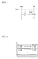
- FIG. 1 is a circuit diagram of a conventional pixel circuit for driving an organic EL element using TFTs. For simplicity reasons, only one of the N ⁇ M pixels is shown in FIG. 1.
- a current-driven transistor M2 is coupled to the organic EL element (OLED) to supply a current for light emission.
- the amount of current of the current-driven transistor M2 is controlled by the data voltage applied through a switching transistor M1.
- a capacitor Cst for sustaining the applied voltage for a predetermined time period is coupled between the source and gate of the transistor M2.
- the gate of the transistor M1 is coupled to a selection signal line Select, and the source is coupled to the data line Vdata.
- the data voltage Vdata is applied to the gate of the driving transistor M2 through the data line.
- a current flows to the organic EL element (OLED) through the transistor M2 to emit light.
- I OLED the current flowing to the organic EL element (OLED)
- Vgs the voltage between the source and gate of the transistor M2
- Vth the threshold voltage of the transistor M2
- Vdata the data voltage
- ⁇ is a constant.
- the current corresponding to the applied data voltage Vdata is supplied to the organic EL element (OLED), which emits light by the supplied current.
- OLED organic EL element
- the pixel driving voltage Vdd is constructed as a horizontal or vertical line for supplying the power to the driving transistor of each cell.
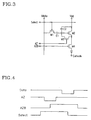
- the pixel driving voltage Vdd is constructed as a horizontal line as illustrated in FIG. 2 and there are many turned-on driving transistors in the cell coupled to each branched Vdd line, a high current flows to the corresponding Vdd line, and the voltage difference between the right and left sides of the line increases.
- This voltage drop in the voltage line Vdd is proportional to the amount of current, which is dependent upon the number of turned-on pixels among the pixels coupled to the corresponding line. So, the voltage drop is also changed depending on the number of turned-on pixels.
- the driving voltage Vdd applied to the right-handed pixel of the line is lower than the driving voltage Vdd applied to the left-handed pixel
- the voltage Vgs applied to the driving transistor located at the right-handed pixel is lower than the voltage Vgs applied to the driving transistor at the left-handed pixel, thereby causing a difference in the amount of current flowing to the transistors and hence a brightness difference.
- the amount of current supplied to the organic EL element (OLED) changes causing a brightness difference, due to changes in the threshold voltage Vth of the TFT. Changes in the threshold voltage Vth of the TFT occurs due to the non-uniformity of the manufacturing process.
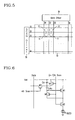
- FIG. 3 is a circuit diagram of a pixel circuit derived to solve the above problem and to avoid the non-uniformity of brightness caused by the variation of the threshold voltage Vth of the driving transistor.
- FIG. 4 is a driving timing diagram for the circuit of FIG. 3.
- the data voltage for the driving transistor M2 must be equal to the driving voltage Vdd while AZ signal is LOW.
- the present invention is an organic EL display that compensates for the deviation of the threshold voltage of a TFT driving transistor to represent uniform brightness.
- the present invention is an organic EL display that compensates for the difference in the voltage drop among pixels caused in the driving voltage Vdd line to represent uniform brightness.
- a luminescent display includes: a plurality of data lines each of the plurality of data lines transferring a data signal representing an image signal; a plurality of scan lines each of the plurality of scan lines transferring a selection signal thereon; a plurality of pixel circuits formed at a corresponding pixel of a plurality of pixels defined by the plurality of data lines and the plural scan lines; and a power supply line coupled to each pixel circuit.
- Each pixel circuit includes: a luminescent element for emitting light corresponding to an amount of current applied; a first capacitor; a first transistor having a control electrode thereof coupled to the first capacitor, and a first main electrode thereof coupled to the power supply line; a first switch for diode-connecting the first transistor in response to a selection signal from a previous scan line for a pixel that was previously scanned to charge the first capacitor with a voltage corresponding to a threshold voltage of the first transistor; a second transistor for transferring the data signal from the data lines in response to a selection signal from a present scan line for a pixel that is being presently scanned; a second capacitor coupled between the power supply line and the second transistor for storing a voltage corresponding to the data signal; and a second switch for electrically isolating a second main electrode of the first transistor from the luminescent element during voltage-charging of the first capacitor in response to a control signal.
- the first transistor supplies a current corresponding to the sum of the voltages charged in the first and second capacitor
- the first switch includes: a third transistor coupled between the power supply line and the first capacitor for applying a voltage from the power supply line to the first capacitor in response to the selection signal from the previous scan line; and a fourth transistor coupled between a control electrode and the second main electrode of the first transistor for diode-connecting the control and first main electrodes of the first transistor in response to the selection signal from the previous scan line.
- the second to fourth transistors are transistors of the same conductivity type.
- control signal is the selection signal from the previous scan line.
- the second switch includes a third transistor that is turned off in response to the control signal and coupled between the second main electrode of the first transistor and the luminescent element.
- the second switch includes a third transistor coupled between the second main electrode of the first transistor and the luminescent element.
- the control signal is a selection signal from a separate scan line, and it turns on the third transistor.
- control signal includes the selection signal from the previous scan line, and the selection signal from the present scan line.
- the second switch includes third and fourth transistors that are coupled in series between the second main electrode of the first transistor and the luminescent element, and that have a control electrode thereof coupled to the previous scan line and the present scan line, respectively.
- a pixel circuit for a luminescent display in which plural pixel circuits are formed in a plurality of pixels defined by a plurality of data lines and a plurality of scan lines
- the pixel circuit includes: a luminescent element; a first transistor having a first main electrode thereof coupled to a power supply line, and supplying a current for light-emission of the luminescent element; first and second capacitors coupled in series between the power supply line and the control electrode of the first transistor; a second transistor having a control electrode thereof coupled to a present scan line for a pixel that is being presently scanned, and a first and a second main electrodes thereof coupled to the data line and the first and second capacitors, respectively; a third transistor having a control electrode thereof coupled to a previous scan line for a pixel that was previously scanned, and coupled between the power supply line and the first and second capacitors; and a fourth transistor having a control electrode thereof coupled to the previous scan line, and being coupled between the second
- the third and fourth transistors are transistors of the same conductivity type.
- the pixel circuit further includes a switch coupled between the first transistor and the luminescent element having a control terminal thereof for receiving a control signal.
- control signal is a selection signal from the previous scan line.
- the switch includes a fifth transistor coupled between a second main electrode of the first transistor and the luminescent element and that is turned off in response to the control signal.
- the switch includes a fifth transistor coupled between the second main electrode of the first transistor and the luminescent element.
- the control signal is a selection signal from a separate scan line for turning on the fifth transistor.
- control signal includes a selection signal from the previous scan line and a selection signal from the present scan line.
- the switch includes fifth and sixth transistors having a gate electrode thereof coupled to the previous scan line and the scan line. The fifth and sixth transistors are coupled in series between the second main electrode of the first transistor and the luminescent element.
- a method for driving a luminescent display which includes a data line, a scan line intersecting the data lines, and a pixel formed in area defined by the data line and the scan line and having a transistor for supplying a current to a luminescent element.
- the method includes: compensating a gate voltage of the transistor in response to a previous selection signal for selecting a first pixel that was previously scanned coupled to a previous scan line; applying a selection signal for selecting the pixel coupled to the scan line; and receiving the data voltage from the data line in response to the selection signal, and supplying a current corresponding to the sum of the compensated gate voltage and the data voltage to the luminescent element.
- the method further includes: interrupting a supply of the current to the luminescent element while the data voltage is applied from the data line in response to the control signal.
- control signal is the selection signal, or a selection signal from a separate scan line.
- a display device comprising: a display element for displaying a portion of an image in response to a current being applied; a transistor having a first main electrode coupled to a voltage source; a first capacitor coupled to a control electrode of the first transistor for charging a first voltage corresponding to a threshold voltage of the transistor; and a first switch coupled between a second main electrode of the transistor and the display element for intercepting the current supplied to the display element from the transistor.
- the first voltage is charged in the first capacitor during a first period
- the second voltage is charged in the second capacitor during a second period.
- the first and second periods may not be superimposed.
- the first switch intercepts the current during the first period or the second period.
- the display device comprises a second switch coupled in parallel to the second capacitor, and the second switch is turned on to discharge the second capacitor.
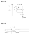
- FIG. 5 is a schematic plan diagram of an organic EL display according to an embodiment of the present invention.
- the organic EL display according to the embodiment of the present invention comprises, as shown in FIG. 5, an organic EL display panel 10, a scan driver 20, and a data driver 30.
- the organic EL display panel 10 comprises a plurality of data lines D 1 to D y for transferring data signals representing image signals; a plurality of scan lines S 1 to S z for transferring selection signals; and a plurality of pixel circuits 11, each formed in a pixel area defined by two adjacent data lines and two adjacent scan lines.
- the data driver 30 applies a data voltage representing image signals to the plural data lines D 1 to D y
- the scan driver 20 sequentially applies the selection signal to the plural scan lines S 1 to S z .
- FIG. 6 is a circuit diagram of a pixel circuit 11 according to a first embodiment of the present invention.
- the pixel circuit 11 comprises, as shown in FIG. 6, an organic EL element (OLED), transistors M1 to M5, and capacitors Cst and Cvth according to the first embodiment of the present invention.
- OLED organic EL element
- the organic EL element emits light corresponding to the amount of current applied.
- the current-driven transistor M1 has a source electrode, which is one of two main electrodes, coupled to a driving voltage Vdd, and a drain electrode, which is the other main electrode, coupled to the source electrode of the transistor M2.
- the transistor M1 outputs a driving current corresponding to the voltage applied between its gate and source.
- the selection transistor M3 has a drain electrode, which is one of two main electrodes, coupled to the source electrode, which is the other main electrode of the transistor M4, a source electrode coupled to the data line Data, and a gate electrode, which is a control electrode, coupled to the n-th scan line.
- the drain electrode of the transistor M4 is coupled to the voltage Vdd.
- the gate electrodes of the transistors M2, M4, and M5 are coupled to the (n-1)-th scan line.
- the current-supplying transistor M1 and the selection transistors M3, M4, and M5 are all PMOS type TFTs, and the selection transistor M2 is an NMOS TFT.
- the capacitors Cst and Cvth are coupled in series between the driving voltage Vdd and the gate of the transistor M1.
- the data line Data is coupled between the capacitors Cst and Cvth through the selection transistor M3.
- FIG. 6 Next, the operation of the pixel circuit according to the first embodiment of the present invention in FIG. 6 will be described with reference to FIGS. 7A, 7B, 8A, and 8B.
- the previous scan line for a pixel that was scanned previous to the pixel that is being presently scanned i.e., the (n-1)-th, or previous scan line
- the transistors M4 and M5 are turned on and the transistor M2 is turned off, as shown in FIG. 7A.
- the transistor M3having its gate coupled to the n-th scan line is turned off.
- the transistor M4 having its gate and source shorted, performs a diode function for the driving voltage Vdd.
- the threshold voltage Vth of the transistor M1 is thus stored in the capacitor Cvth, because the capacitor Cst is shorted by the turned on transistor M4.
- the n-th scan line (nth Scan) is selected to apply a low signal to the n-th scan line and a high signal to the (n-1)-th scan line ((n-1 )th Scan).
- the transistors M4 and M5 are turned off and the transistor M2 is turned on, as shown in FIG. 8A.
- the transistor M3 having its gate coupled to the n-th scan line (nth Scan) is also turned on. Due to the data voltage Vdata from the data line Data, the voltage of the node D is changed to the data voltage Vdata.
- the gate voltage of the transistor M1 amounts to Vdata - Vth, because the threshold voltage Vth of the transistor M1 is stored in the capacitor Cvth.
- the gate-source voltage of the transistor M1 is given by the equation 3, and the current I OLED of the equation 4 is supplied to the organic EL element (OLED) through the transistor M1.
- Vgs Vdd - ( Vdata-Vth )
- the data voltage Vdata compensates for the deviation of the threshold voltage Vth to supply a constant current supplied to the organic EL element (OLED), thus solving the problem with the non-uniformity of brightness according to the position of the pixel.
- the driving voltage Vdd drops due to the resistance of the supply line of the driving voltage Vdd.
- the voltage drop in this case is proportional to the amount of current flowing to the supply line of the driving voltage Vdd. Accordingly, with the same data voltage Vdata applied, the voltage Vgs applied to the driving transistor is changed to vary the current, causing non-uniformity of brightness.
- FIG. 9A is a circuit diagram of a pixel circuit according to a second embodiment of the present invention that prevents a change of the voltage Vgs (of the M1 transistor) by interrupting the current to the driving transistor M1 while the data voltage Vdata is applied, in the case where the supply line of the driving voltage Vdd is arranged in the same direction as the scan line.
- FIG. 9B is a scan timing diagram of the pixel circuit of FIG. 9A.
- the NMOS transistor M2 the gate of which is coupled to the previous scan line ((n-1)th Scan) in the circuit of FIG 6, is replaced with the PMOS transistor M2 and a separate scan line (nth Scan2) for controlling the transistor M2 is connected to the gate of the new transistor M2.
- a high signal is applied to the scan line (nth Scan2) while a low signal is sequentially applied to the (n-1)-th and n-th scan lines ((n-1)th Scan and nth Scan), to turn the transistor M2 off.
- a low signal is sequentially applied to the (n-1)-th and n-th scan lines ((n-1)th Scan and nth Scan), to turn the transistor M2 off.
- current is prevented from flowing to the transistor M1 while the data voltage Vdata is applied.
- the circuit of FIG. 9A which has a separate scan line for controlling the transistor M2, requires a circuit for generating a signal to be applied to this scan line.
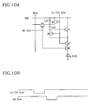
- FIG. 10A is a circuit diagram of a pixel circuit according to a third embodiment of the present invention which does not require a circuit for generating a new signal.
- FIG. 10B is a scan timing diagram of the circuit of FIG. 10A.
- the pixel circuit according to the third embodiment of the present invention adds, as illustrated in FIG. 10A, an NMOS transistor M6 between the transistor M2 and the organic EL element (OLED) of the circuit of FIG. 6.
- the gate of the transistor M6 is coupled to the n-th scan line (nth Scan).
- the transistor M2 is short-circuited with a low signal applied to the (n-1)-th scan line ((n-1)th Scan), and the transistor M6 is short-circuited with a low signal applied to the n-th scan line (nth Scan), thereby preventing a current flowing to the transistor M1 while the data voltage Vdata is applied.
- the transistor M6 may be disposed at any position between the driving voltage Vdd and the cathode power source.
- the present invention effectively compensates for the deviation of the threshold voltage of the TFT for driving an organic EL element to prevent non-uniformity of brightness.
- the present invention prevents non-uniformity of brightness caused by a voltage drop of the driving power line when the driving power line is arranged in the same direction of the scan line.
Landscapes
- Engineering & Computer Science (AREA)
- Physics & Mathematics (AREA)
- Computer Hardware Design (AREA)
- General Physics & Mathematics (AREA)
- Theoretical Computer Science (AREA)
- Control Of Indicators Other Than Cathode Ray Tubes (AREA)
- Control Of El Displays (AREA)
- Electroluminescent Light Sources (AREA)
- Devices For Indicating Variable Information By Combining Individual Elements (AREA)
Abstract
Description
Claims (22)
- A luminescent display comprising:a plurality of data lines for transferring thereon a data signal representing an image;a plurality of scan lines, each of the plurality of scan lines transferring a selection signal;a plurality of pixel circuits, each of the plurality of pixel circuits formed at a corresponding pixel of a plurality of pixels defined by the plural data lines and the plurality of scan lines; anda power supply line coupled to each of the plurality of pixel circuits,each of the plurality of pixel circuits comprising:a luminescent element for emitting light corresponding to an amount of current applied;a first capacitor;a first transistor having a control electrode thereof coupled to the first capacitor, and a first main electrode thereof coupled to the power supply line;a first switch for diode-connecting the first transistor in response to a selection signal from a previous scan line for a pixel that was previously scanned to charge the first capacitor with a voltage corresponding to a threshold voltage of the first transistor;a second transistor for transferring the data signal from the data tines in response to a selection signal from a present scan line for a pixel that is being presently scanned;a second capacitor coupled between the power supply line and the second transistor for storing a voltage corresponding to the data signal; anda second switch for electrically isolating a second main electrode of the first transistor from the luminescent element during voltage-charging of the first capacitor in response to a control signal,the first transistor supplying a current corresponding to the sum of the voltages charged in the first and second capacitors.
- The luminescent display as claimed in claim 1, wherein the first switch comprises:a third transistor for applying a voltage from the power supply line to the first capacitor in response to the selection signal from the previous scan line; anda fourth transistor for diode-connecting the first transistor in response to the selection signal from the previous scan line.
- The luminescent display as claimed in claim 2, wherein the second, third, and fourth transistors are transistors of the same conductivity type.
- The luminescent display as claimed in claim 1, wherein the control signal is the selection signal from the previous scan line, and
the second switch comprises a third transistor being turned off in response to the control signal and coupled between the first transistor and the luminescent element. - The luminescent display as claimed in claim 1, wherein the second switch comprises a third transistor coupled between the first transistor and the luminescent element, and
the control signal is a selection signal from a separate scan line for turning on the third transistor. - The luminescent display as claimed in claim 1, wherein the control signal includes the selection signal from the previous scan line, and the selection signal from the present scan line, and
the second switch comprises third and fourth transistors coupled in series between the first transistor and the luminescent element and having their control electrodes coupled to the previous scan line and the present scan line, respectively. - A pixel circuit for a luminescent display, in which plural pixel circuits are formed in a plurality of pixels defined by a plurality of data lines and a plurality of scan lines, each pixel circuit comprising:a luminescent element;a first transistor having a first main electrode thereof coupled to a power supply line, and supplying a current for light-emission of the luminescent element;first and second capacitors coupled in series between the power supply line and the control electrode of the first transistor;a second transistor having a control electrode thereof coupled to a present scan line for a pixel that is being presently scanned, and a first and a second main electrodes thereof coupled to a data line of the plurality of data lines and the first and second capacitors, respectively;a third transistor having a control electrode thereof coupled to a previous scan line for a pixel that was previously scanned, and coupled between the power supply line and the first and second capacitors; anda fourth transistor having a control electrode thereof coupled to the previous scan line, and being coupled between the second capacitor and the second main electrode of the first transistor,the first transistor supplying a current corresponding to a voltage charged in the first and second capacitors.
- The pixel circuit as claimed in claim 7, wherein the third and fourth transistors are transistors of the same conductivity type.
- The pixel circuit as claimed in claim 7, further comprising:a switch coupled between the first transistor and the luminescent element having a control terminal thereof for receiving a control signal.
- The pixel circuit as claimed in claim 9, wherein the control signal is a selection signal from the previous scan line, and
the switch comprises a fifth transistor coupled between the first transistor and the luminescent element and being turned off in response to the control signal. - The pixel circuit as claimed in claim 9, wherein the switch comprises a fifth transistor coupled between the first transistor and the luminescent element, and
the control signal is a selection signal from a separate scan line for turning on the fifth transistor. - The pixel circuit as claimed in claim 9, wherein the control signal includes a selection signal from the previous scan line and a selection signal from the present scan line, and
the switch comprises fifth and sixth transistors each having a gate electrode thereof coupled to the previous scan line and the present scan line, respectively, the fifth and sixth transistors being coupled in series between the first transistor and the luminescent element. - A method for driving a luminescent display, which includes a data line, a scan line intersecting the data line, and a pixel formed in an area defined by the data line and the scan line and having a transistor for supplying a current to a luminescent element, the method comprising:compensating a gate voltage of the transistor in response to a previous selection signal for selecting a first pixel coupled to a previous scan line for a pixel that was previously scanned;applying a selection signal for selecting the pixel coupled to the scan line; andreceiving the data voltage from the data line in response to the selection signal, and supplying a current corresponding to the sum of the compensated gate voltage and the data voltage to the luminescent element.
- The method as claimed in claim 13, further comprising:interrupting a supply of the current to the luminescent element while the data voltage is applied from the data line, in response to the control signal.
- The method as claimed in claim 14, wherein the control signal is the previous selection signal.
- The method as claimed in claim 14, wherein the control signal is a selection signal from a separate scan line.
- A display device comprising:a display element for displaying a portion of an image in response to a current being applied;a transistor having a main electrode coupled to a voltage source;a first capacitor for charging a first voltage corresponding to a threshold voltage of the transistor; anda first switch, coupled between the transistor and the display element for intercepting a current supplied to the display element from the transistor.
- The display device of claim 17, wherein a first voltage is charged in the first capacitor during a first period, and a second voltage is charged in a second capacitor during a second period.
- The display device of claim 18, wherein the first and second periods are not superimposed.
- The display device of claim 18, wherein the first switch intercepts the current supplied to the display element during the first period.
- The display device of claim 18, wherein the first switch intercepts the current supplied to the display element during the second period.
- The display device of claim 18, further comprising a second switch coupled in parallel to the second capacitor, wherein the second switch is turned on to discharge the second capacitor.
Applications Claiming Priority (2)
| Application Number | Priority Date | Filing Date | Title |
|---|---|---|---|
| KR2003003975 | 2003-01-21 | ||
| KR10-2003-0003975A KR100490622B1 (en) | 2003-01-21 | 2003-01-21 | Organic electroluminescent display and driving method and pixel circuit thereof |
Publications (3)
| Publication Number | Publication Date |
|---|---|
| EP1441325A2 true EP1441325A2 (en) | 2004-07-28 |
| EP1441325A3 EP1441325A3 (en) | 2004-12-29 |
| EP1441325B1 EP1441325B1 (en) | 2006-06-14 |
Family
ID=36650867
Family Applications (1)
| Application Number | Title | Priority Date | Filing Date |
|---|---|---|---|
| EP03090421A Expired - Lifetime EP1441325B1 (en) | 2003-01-21 | 2003-12-03 | Luminescent display, driving method and pixel circuit thereof |
Country Status (7)
| Country | Link |
|---|---|
| US (1) | US7277071B2 (en) |
| EP (1) | EP1441325B1 (en) |
| JP (1) | JP4197476B2 (en) |
| KR (1) | KR100490622B1 (en) |
| CN (1) | CN1312651C (en) |
| AT (1) | ATE330307T1 (en) |
| DE (1) | DE60306094T2 (en) |
Cited By (17)
| Publication number | Priority date | Publication date | Assignee | Title |
|---|---|---|---|---|
| EP1585100A1 (en) | 2004-03-10 | 2005-10-12 | Samsung SDI Co., Ltd. | Electroluminescent display device, pixel circuit therefor, and driving method thereof |
| EP1628285A1 (en) | 2004-08-20 | 2006-02-22 | Samsung SDI Co., Ltd. | Method for managing display data of a light emitting display |
| EP1630784A1 (en) * | 2004-08-30 | 2006-03-01 | Samsung SDI Co., Ltd. | Frame memory driving method |
| EP1640965A1 (en) * | 2004-09-24 | 2006-03-29 | Samsung SDI Co., Ltd. | Light emitting display |
| WO2006054189A1 (en) * | 2004-11-16 | 2006-05-26 | Koninklijke Philips Electronics N.V. | Active matrix display devices |
| EP1679687A2 (en) | 2005-01-05 | 2006-07-12 | Samsung SDI Co., Ltd. | Display device and driving method thereof |
| CN100373436C (en) * | 2004-08-02 | 2008-03-05 | 统宝光电股份有限公司 | pixel driving circuit and method for driving display component |
| US7616177B2 (en) | 2004-08-02 | 2009-11-10 | Tpo Displays Corp. | Pixel driving circuit with threshold voltage compensation |
| CN101515435B (en) * | 2008-02-19 | 2012-01-11 | 乐金显示有限公司 | Organic light emitting diode display |
| CN101520986B (en) * | 2008-02-28 | 2012-03-21 | 索尼株式会社 | El display panel, electronic apparatus and el display panel driving method |
| CN103050080A (en) * | 2011-10-11 | 2013-04-17 | 上海天马微电子有限公司 | Pixel circuit of organic light emitting display and driving method thereof |
| US8547300B2 (en) | 2004-06-30 | 2013-10-01 | Samsung Display Co., Ltd. | Light emitting display and display panel and driving method thereof |
| CN103700342A (en) * | 2013-12-12 | 2014-04-02 | 京东方科技集团股份有限公司 | OLED (Organic Light-Emitting Diode) pixel circuit, driving method and display device |
| US8743030B2 (en) | 2005-09-16 | 2014-06-03 | Semiconductor Energy Laboratory Co., Ltd. | Display device and driving method of display device |
| EP2996108A3 (en) * | 2003-05-23 | 2016-04-06 | Sony Corporation | Pixel circuit, display device, and method of driving pixel circuit |
| CN105810151A (en) * | 2016-05-31 | 2016-07-27 | 上海天马微电子有限公司 | Pixel driving circuit, driving method, display panel and display device |
| CN107293258A (en) * | 2017-07-03 | 2017-10-24 | 武汉华星光电半导体显示技术有限公司 | The compensation circuit of OLED display and OLED |
Families Citing this family (205)
| Publication number | Priority date | Publication date | Assignee | Title |
|---|---|---|---|---|
| US7569849B2 (en) | 2001-02-16 | 2009-08-04 | Ignis Innovation Inc. | Pixel driver circuit and pixel circuit having the pixel driver circuit |
| JP4307830B2 (en) * | 2002-12-25 | 2009-08-05 | 株式会社半導体エネルギー研究所 | Image display device |
| CA2419704A1 (en) | 2003-02-24 | 2004-08-24 | Ignis Innovation Inc. | Method of manufacturing a pixel with organic light-emitting diode |
| KR100502912B1 (en) * | 2003-04-01 | 2005-07-21 | 삼성에스디아이 주식회사 | Light emitting display device and display panel and driving method thereof |
| KR100560780B1 (en) * | 2003-07-07 | 2006-03-13 | 삼성에스디아이 주식회사 | Pixel circuit of organic light emitting display device and driving method thereof |
| CA2443206A1 (en) | 2003-09-23 | 2005-03-23 | Ignis Innovation Inc. | Amoled display backplanes - pixel driver circuits, array architecture, and external compensation |
| KR100515305B1 (en) * | 2003-10-29 | 2005-09-15 | 삼성에스디아이 주식회사 | Light emitting display device and display panel and driving method thereof |
| JP4147410B2 (en) * | 2003-12-02 | 2008-09-10 | ソニー株式会社 | Transistor circuit, pixel circuit, display device, and driving method thereof |
| GB0400213D0 (en) * | 2004-01-07 | 2004-02-11 | Koninkl Philips Electronics Nv | Electroluminescent display devices |
| KR100560444B1 (en) * | 2004-03-24 | 2006-03-13 | 삼성에스디아이 주식회사 | Light emitting display device and driving method thereof |
| JP5121124B2 (en) * | 2005-03-28 | 2013-01-16 | 三洋電機株式会社 | Organic EL pixel circuit |
| JP4999281B2 (en) * | 2005-03-28 | 2012-08-15 | 三洋電機株式会社 | Organic EL pixel circuit |
| JP4401971B2 (en) * | 2004-04-29 | 2010-01-20 | 三星モバイルディスプレイ株式會社 | Luminescent display device |
| KR100560450B1 (en) * | 2004-04-29 | 2006-03-13 | 삼성에스디아이 주식회사 | Light emitting display panel and light emitting display device |
| KR100560449B1 (en) * | 2004-04-29 | 2006-03-13 | 삼성에스디아이 주식회사 | Light emitting display panel and light emitting display device |
| US8378930B2 (en) | 2004-05-28 | 2013-02-19 | Sony Corporation | Pixel circuit and display device having symmetric pixel circuits and shared voltage lines |
| KR100658616B1 (en) * | 2004-05-31 | 2006-12-15 | 삼성에스디아이 주식회사 | Light emitting display device, display panel and driving method thereof |
| DE102004028233A1 (en) * | 2004-06-11 | 2005-12-29 | Deutsche Thomson-Brandt Gmbh | Method for controlling and switching an element of a light-emitting display |
| KR100646935B1 (en) * | 2004-06-24 | 2006-11-23 | 삼성에스디아이 주식회사 | Light emitting display |
| KR100698681B1 (en) * | 2004-06-29 | 2007-03-23 | 삼성에스디아이 주식회사 | Light emitting display |
| CA2472671A1 (en) | 2004-06-29 | 2005-12-29 | Ignis Innovation Inc. | Voltage-programming scheme for current-driven amoled displays |
| KR100578813B1 (en) * | 2004-06-29 | 2006-05-11 | 삼성에스디아이 주식회사 | Light emitting display device and driving method thereof |
| US8199079B2 (en) * | 2004-08-25 | 2012-06-12 | Samsung Mobile Display Co., Ltd. | Demultiplexing circuit, light emitting display using the same, and driving method thereof |
| KR100570781B1 (en) | 2004-08-26 | 2006-04-12 | 삼성에스디아이 주식회사 | Organic electroluminescent display, display panel and driving method thereof |
| KR100673759B1 (en) * | 2004-08-30 | 2007-01-24 | 삼성에스디아이 주식회사 | Light emitting display |
| KR100590042B1 (en) * | 2004-08-30 | 2006-06-14 | 삼성에스디아이 주식회사 | Light emitting display device, driving method and signal driving device |
| JP4160032B2 (en) | 2004-09-01 | 2008-10-01 | シャープ株式会社 | Display device and driving method thereof |
| KR100673760B1 (en) * | 2004-09-08 | 2007-01-24 | 삼성에스디아이 주식회사 | Light emitting display |
| KR100684714B1 (en) * | 2004-09-15 | 2007-02-20 | 삼성에스디아이 주식회사 | Light emitting display device and driving method thereof |
| JP4192133B2 (en) * | 2004-09-28 | 2008-12-03 | 東芝松下ディスプレイテクノロジー株式会社 | Display device and driving method thereof |
| KR20060054603A (en) * | 2004-11-15 | 2006-05-23 | 삼성전자주식회사 | Display device and driving method thereof |
| JP4437110B2 (en) * | 2004-11-17 | 2010-03-24 | 三星モバイルディスプレイ株式會社 | Organic light emitting display device, driving method of organic light emitting display device, and driving method of pixel circuit |
| KR100606416B1 (en) * | 2004-11-17 | 2006-07-31 | 엘지.필립스 엘시디 주식회사 | Driving device and driving method of organic light emitting diode |
| KR100739316B1 (en) * | 2004-11-17 | 2007-07-12 | 삼성에스디아이 주식회사 | Light emitting display device and driving method thereof |
| CA2490858A1 (en) | 2004-12-07 | 2006-06-07 | Ignis Innovation Inc. | Driving method for compensated voltage-programming of amoled displays |
| KR100604060B1 (en) * | 2004-12-08 | 2006-07-24 | 삼성에스디아이 주식회사 | Light emitting display device and driving method thereof |
| KR100698697B1 (en) * | 2004-12-09 | 2007-03-23 | 삼성에스디아이 주식회사 | Light emitting display device and manufacturing method thereof |
| KR100623813B1 (en) * | 2004-12-10 | 2006-09-19 | 엘지.필립스 엘시디 주식회사 | Organic EL device and driving method thereof |
| US9275579B2 (en) | 2004-12-15 | 2016-03-01 | Ignis Innovation Inc. | System and methods for extraction of threshold and mobility parameters in AMOLED displays |
| US20140111567A1 (en) | 2005-04-12 | 2014-04-24 | Ignis Innovation Inc. | System and method for compensation of non-uniformities in light emitting device displays |
| TWI402790B (en) | 2004-12-15 | 2013-07-21 | 伊格尼斯創新股份有限公司 | Method and system for programming, calibrating and driving a light-emitting element display |
| US9280933B2 (en) | 2004-12-15 | 2016-03-08 | Ignis Innovation Inc. | System and methods for extraction of threshold and mobility parameters in AMOLED displays |
| US8576217B2 (en) | 2011-05-20 | 2013-11-05 | Ignis Innovation Inc. | System and methods for extraction of threshold and mobility parameters in AMOLED displays |
| US9171500B2 (en) | 2011-05-20 | 2015-10-27 | Ignis Innovation Inc. | System and methods for extraction of parasitic parameters in AMOLED displays |
| US10012678B2 (en) | 2004-12-15 | 2018-07-03 | Ignis Innovation Inc. | Method and system for programming, calibrating and/or compensating, and driving an LED display |
| US9799246B2 (en) | 2011-05-20 | 2017-10-24 | Ignis Innovation Inc. | System and methods for extraction of threshold and mobility parameters in AMOLED displays |
| US10013907B2 (en) | 2004-12-15 | 2018-07-03 | Ignis Innovation Inc. | Method and system for programming, calibrating and/or compensating, and driving an LED display |
| KR100604066B1 (en) * | 2004-12-24 | 2006-07-24 | 삼성에스디아이 주식회사 | Pixel and light emitting display device using same |
| CA2495726A1 (en) | 2005-01-28 | 2006-07-28 | Ignis Innovation Inc. | Locally referenced voltage programmed pixel for amoled displays |
| CA2496642A1 (en) | 2005-02-10 | 2006-08-10 | Ignis Innovation Inc. | Fast settling time driving method for organic light-emitting diode (oled) displays based on current programming |
| KR101152120B1 (en) * | 2005-03-16 | 2012-06-15 | 삼성전자주식회사 | Display device and driving method thereof |
| KR100707623B1 (en) | 2005-03-19 | 2007-04-13 | 한양대학교 산학협력단 | Pixel and light emitting display device using same |
| KR20060109343A (en) | 2005-04-15 | 2006-10-19 | 세이코 엡슨 가부시키가이샤 | Electronic circuits, their driving methods, electro-optical devices, and electronic devices |
| KR100840116B1 (en) * | 2005-04-28 | 2008-06-20 | 삼성에스디아이 주식회사 | Light emitting display |
| KR100761077B1 (en) * | 2005-05-12 | 2007-09-21 | 삼성에스디아이 주식회사 | Organic electroluminescent display |
| US7852298B2 (en) * | 2005-06-08 | 2010-12-14 | Ignis Innovation Inc. | Method and system for driving a light emitting device display |
| CN100514421C (en) * | 2005-06-30 | 2009-07-15 | 中华映管股份有限公司 | Pixel driving circuit and method for organic light emitting display |
| US8629819B2 (en) * | 2005-07-14 | 2014-01-14 | Semiconductor Energy Laboratory Co., Ltd. | Semiconductor device and driving method thereof |
| KR100547515B1 (en) * | 2005-07-27 | 2006-01-31 | 실리콘 디스플레이 (주) | Organic light emitting diode display and driving method |
| KR100635509B1 (en) * | 2005-08-16 | 2006-10-17 | 삼성에스디아이 주식회사 | Organic electroluminescent display |
| KR100627417B1 (en) * | 2005-08-26 | 2006-09-22 | 삼성에스디아이 주식회사 | OLED display and driving method thereof |
| CA2518276A1 (en) * | 2005-09-13 | 2007-03-13 | Ignis Innovation Inc. | Compensation technique for luminance degradation in electro-luminance devices |
| KR100666640B1 (en) * | 2005-09-15 | 2007-01-09 | 삼성에스디아이 주식회사 | Organic electroluminescent display |
| JP5057731B2 (en) * | 2005-09-16 | 2012-10-24 | 株式会社半導体エネルギー研究所 | Display device, module, and electronic device |
| KR101209055B1 (en) | 2005-09-30 | 2012-12-06 | 삼성디스플레이 주식회사 | Display device and driving method thereof |
| KR101324756B1 (en) | 2005-10-18 | 2013-11-05 | 가부시키가이샤 한도오따이 에네루기 켄큐쇼 | Display device and driving method thereof |
| JP5013697B2 (en) * | 2005-10-19 | 2012-08-29 | 三洋電機株式会社 | Display device |
| JP5245195B2 (en) * | 2005-11-14 | 2013-07-24 | ソニー株式会社 | Pixel circuit |
| CN101313349B (en) * | 2005-11-29 | 2010-12-01 | 京瓷株式会社 | image display device |
| EP2458579B1 (en) | 2006-01-09 | 2017-09-20 | Ignis Innovation Inc. | Method and system for driving an active matrix display circuit |
| US9489891B2 (en) | 2006-01-09 | 2016-11-08 | Ignis Innovation Inc. | Method and system for driving an active matrix display circuit |
| US9269322B2 (en) | 2006-01-09 | 2016-02-23 | Ignis Innovation Inc. | Method and system for driving an active matrix display circuit |
| KR100843786B1 (en) * | 2006-03-29 | 2008-07-03 | 비오이 하이디스 테크놀로지 주식회사 | Pixel driving voltage compensation circuit for organic electroluminescent display |
| TW200746022A (en) | 2006-04-19 | 2007-12-16 | Ignis Innovation Inc | Stable driving scheme for active matrix displays |
| KR101186254B1 (en) * | 2006-05-26 | 2012-09-27 | 엘지디스플레이 주식회사 | Organic Light Emitting Diode Display And Driving Method Thereof |
| JP2007316454A (en) | 2006-05-29 | 2007-12-06 | Sony Corp | Image display device |
| KR101202040B1 (en) * | 2006-06-30 | 2012-11-16 | 엘지디스플레이 주식회사 | Organic light emitting diode display and driving method thereof |
| KR100739334B1 (en) * | 2006-08-08 | 2007-07-12 | 삼성에스디아이 주식회사 | Pixel, organic light emitting display device using same, and driving method thereof |
| CA2556961A1 (en) | 2006-08-15 | 2008-02-15 | Ignis Innovation Inc. | Oled compensation technique based on oled capacitance |
| TWI442368B (en) | 2006-10-26 | 2014-06-21 | 半導體能源研究所股份有限公司 | Electronic device, display device, and semiconductor device, and driving method thereof |
| KR100821055B1 (en) * | 2006-12-27 | 2008-04-08 | 삼성에스디아이 주식회사 | Organic light emitting display device and driving method thereof |
| KR100858618B1 (en) * | 2007-04-10 | 2008-09-17 | 삼성에스디아이 주식회사 | Organic light emitting display device and driving method thereof |
| CN101743583B (en) * | 2007-07-19 | 2012-09-19 | 松下电器产业株式会社 | Image display device |
| KR101374483B1 (en) * | 2007-08-06 | 2014-03-14 | 엘지디스플레이 주식회사 | Pixel Circuit of Organic Light Emitting Display |
| KR100889675B1 (en) * | 2007-10-25 | 2009-03-19 | 삼성모바일디스플레이주식회사 | Pixel and organic light emitting display device using the same |
| KR100911976B1 (en) * | 2007-11-23 | 2009-08-13 | 삼성모바일디스플레이주식회사 | Organic light emitting display |
| JP5186950B2 (en) * | 2008-02-28 | 2013-04-24 | ソニー株式会社 | EL display panel, electronic device, and driving method of EL display panel |
| JP5138428B2 (en) * | 2008-03-07 | 2013-02-06 | グローバル・オーエルイーディー・テクノロジー・リミテッド・ライアビリティ・カンパニー | Display device |
| WO2009127065A1 (en) | 2008-04-18 | 2009-10-22 | Ignis Innovation Inc. | System and driving method for light emitting device display |
| KR20090120253A (en) * | 2008-05-19 | 2009-11-24 | 삼성전자주식회사 | Back light unit assembly, display device and dimming method having same |
| CA2637343A1 (en) | 2008-07-29 | 2010-01-29 | Ignis Innovation Inc. | Improving the display source driver |
| JP5627175B2 (en) * | 2008-11-28 | 2014-11-19 | エルジー ディスプレイ カンパニー リミテッド | Image display device |
| US9370075B2 (en) | 2008-12-09 | 2016-06-14 | Ignis Innovation Inc. | System and method for fast compensation programming of pixels in a display |
| CN101807582B (en) * | 2009-02-16 | 2012-08-29 | 元太科技工业股份有限公司 | Flexible pixel array substrate and flexible display |
| US9384698B2 (en) | 2009-11-30 | 2016-07-05 | Ignis Innovation Inc. | System and methods for aging compensation in AMOLED displays |
| CA2688870A1 (en) | 2009-11-30 | 2011-05-30 | Ignis Innovation Inc. | Methode and techniques for improving display uniformity |
| US9311859B2 (en) | 2009-11-30 | 2016-04-12 | Ignis Innovation Inc. | Resetting cycle for aging compensation in AMOLED displays |
| US10319307B2 (en) | 2009-06-16 | 2019-06-11 | Ignis Innovation Inc. | Display system with compensation techniques and/or shared level resources |
| CA2669367A1 (en) | 2009-06-16 | 2010-12-16 | Ignis Innovation Inc | Compensation technique for color shift in displays |
| US8283967B2 (en) | 2009-11-12 | 2012-10-09 | Ignis Innovation Inc. | Stable current source for system integration to display substrate |
| US10867536B2 (en) | 2013-04-22 | 2020-12-15 | Ignis Innovation Inc. | Inspection system for OLED display panels |
| US10996258B2 (en) | 2009-11-30 | 2021-05-04 | Ignis Innovation Inc. | Defect detection and correction of pixel circuits for AMOLED displays |
| US8803417B2 (en) | 2009-12-01 | 2014-08-12 | Ignis Innovation Inc. | High resolution pixel architecture |
| CA2687631A1 (en) | 2009-12-06 | 2011-06-06 | Ignis Innovation Inc | Low power driving scheme for display applications |
| US20140313111A1 (en) | 2010-02-04 | 2014-10-23 | Ignis Innovation Inc. | System and methods for extracting correlation curves for an organic light emitting device |
| US10176736B2 (en) | 2010-02-04 | 2019-01-08 | Ignis Innovation Inc. | System and methods for extracting correlation curves for an organic light emitting device |
| CA2692097A1 (en) | 2010-02-04 | 2011-08-04 | Ignis Innovation Inc. | Extracting correlation curves for light emitting device |
| US10163401B2 (en) | 2010-02-04 | 2018-12-25 | Ignis Innovation Inc. | System and methods for extracting correlation curves for an organic light emitting device |
| US10089921B2 (en) | 2010-02-04 | 2018-10-02 | Ignis Innovation Inc. | System and methods for extracting correlation curves for an organic light emitting device |
| US9881532B2 (en) | 2010-02-04 | 2018-01-30 | Ignis Innovation Inc. | System and method for extracting correlation curves for an organic light emitting device |
| CA2696778A1 (en) | 2010-03-17 | 2011-09-17 | Ignis Innovation Inc. | Lifetime, uniformity, parameter extraction methods |
| US8300039B2 (en) * | 2010-03-30 | 2012-10-30 | Sony Corporation | Inverter circuit and display |
| JP2011217175A (en) * | 2010-03-31 | 2011-10-27 | Sony Corp | Inverter circuit and display device |
| JP5488817B2 (en) * | 2010-04-01 | 2014-05-14 | ソニー株式会社 | Inverter circuit and display device |
| JP2011217287A (en) * | 2010-04-01 | 2011-10-27 | Sony Corp | Inverter circuit and display device |
| TW201218163A (en) * | 2010-10-22 | 2012-05-01 | Au Optronics Corp | Driving circuit for pixels of an active matrix organic light-emitting diode display and method for driving pixels of an active matrix organic light-emitting diode display |
| US8907991B2 (en) | 2010-12-02 | 2014-12-09 | Ignis Innovation Inc. | System and methods for thermal compensation in AMOLED displays |
| US20140368491A1 (en) | 2013-03-08 | 2014-12-18 | Ignis Innovation Inc. | Pixel circuits for amoled displays |
| US9886899B2 (en) | 2011-05-17 | 2018-02-06 | Ignis Innovation Inc. | Pixel Circuits for AMOLED displays |
| US9606607B2 (en) | 2011-05-17 | 2017-03-28 | Ignis Innovation Inc. | Systems and methods for display systems with dynamic power control |
| US9351368B2 (en) | 2013-03-08 | 2016-05-24 | Ignis Innovation Inc. | Pixel circuits for AMOLED displays |
| US9134825B2 (en) | 2011-05-17 | 2015-09-15 | Ignis Innovation Inc. | Systems and methods for display systems with dynamic power control |
| US9530349B2 (en) | 2011-05-20 | 2016-12-27 | Ignis Innovations Inc. | Charged-based compensation and parameter extraction in AMOLED displays |
| US9466240B2 (en) | 2011-05-26 | 2016-10-11 | Ignis Innovation Inc. | Adaptive feedback system for compensating for aging pixel areas with enhanced estimation speed |
| WO2012164475A2 (en) | 2011-05-27 | 2012-12-06 | Ignis Innovation Inc. | Systems and methods for aging compensation in amoled displays |
| WO2012164474A2 (en) | 2011-05-28 | 2012-12-06 | Ignis Innovation Inc. | System and method for fast compensation programming of pixels in a display |
| KR101870925B1 (en) * | 2011-06-30 | 2018-06-26 | 삼성디스플레이 주식회사 | Pixel and Organic Light Emitting Display Device Using the same |
| US8901579B2 (en) | 2011-08-03 | 2014-12-02 | Ignis Innovation Inc. | Organic light emitting diode and method of manufacturing |
| US9070775B2 (en) | 2011-08-03 | 2015-06-30 | Ignis Innovations Inc. | Thin film transistor |
| TWI442374B (en) * | 2011-08-16 | 2014-06-21 | 瀚宇彩晶股份有限公司 | Organic light-emitting diode compensation circuit |
| JP6050054B2 (en) | 2011-09-09 | 2016-12-21 | 株式会社半導体エネルギー研究所 | Semiconductor device |
| KR20130046006A (en) * | 2011-10-27 | 2013-05-07 | 삼성디스플레이 주식회사 | Pixel circuit, organic light emitting display device having the same, and method of driving organic light emitting display device |
| KR101549284B1 (en) * | 2011-11-08 | 2015-09-02 | 엘지디스플레이 주식회사 | Organic light emitting diode display device |
| US10089924B2 (en) | 2011-11-29 | 2018-10-02 | Ignis Innovation Inc. | Structural and low-frequency non-uniformity compensation |
| US9324268B2 (en) | 2013-03-15 | 2016-04-26 | Ignis Innovation Inc. | Amoled displays with multiple readout circuits |
| US9385169B2 (en) | 2011-11-29 | 2016-07-05 | Ignis Innovation Inc. | Multi-functional active matrix organic light-emitting diode display |
| US8937632B2 (en) | 2012-02-03 | 2015-01-20 | Ignis Innovation Inc. | Driving system for active-matrix displays |
| US10043794B2 (en) | 2012-03-22 | 2018-08-07 | Semiconductor Energy Laboratory Co., Ltd. | Semiconductor device and electronic device |
| US9747834B2 (en) | 2012-05-11 | 2017-08-29 | Ignis Innovation Inc. | Pixel circuits including feedback capacitors and reset capacitors, and display systems therefore |
| US8922544B2 (en) | 2012-05-23 | 2014-12-30 | Ignis Innovation Inc. | Display systems with compensation for line propagation delay |
| CN102682704A (en) * | 2012-05-31 | 2012-09-19 | 广州新视界光电科技有限公司 | Pixel driving circuit for active organic electroluminescent display and driving method therefor |
| KR101928379B1 (en) * | 2012-06-14 | 2018-12-12 | 엘지디스플레이 주식회사 | Organic light emitting diode display device and method of driving the same |
| KR101341797B1 (en) * | 2012-08-01 | 2013-12-16 | 엘지디스플레이 주식회사 | Organic light emitting diode display device and method for driving the same |
| KR101988355B1 (en) * | 2012-09-10 | 2019-09-25 | 삼성디스플레이 주식회사 | Pixel, display device comprising the same and driving method thereof |
| KR101975000B1 (en) * | 2012-09-13 | 2019-05-07 | 삼성디스플레이 주식회사 | Organic light emitting diode display |
| US9336717B2 (en) | 2012-12-11 | 2016-05-10 | Ignis Innovation Inc. | Pixel circuits for AMOLED displays |
| US9786223B2 (en) | 2012-12-11 | 2017-10-10 | Ignis Innovation Inc. | Pixel circuits for AMOLED displays |
| KR101992405B1 (en) * | 2012-12-13 | 2019-06-25 | 삼성디스플레이 주식회사 | Pixel and Organic Light Emitting Display Device Using the same |
| WO2014108879A1 (en) | 2013-01-14 | 2014-07-17 | Ignis Innovation Inc. | Driving scheme for emissive displays providing compensation for driving transistor variations |
| US9830857B2 (en) | 2013-01-14 | 2017-11-28 | Ignis Innovation Inc. | Cleaning common unwanted signals from pixel measurements in emissive displays |
| US9721505B2 (en) | 2013-03-08 | 2017-08-01 | Ignis Innovation Inc. | Pixel circuits for AMOLED displays |
| CA2894717A1 (en) | 2015-06-19 | 2016-12-19 | Ignis Innovation Inc. | Optoelectronic device characterization in array with shared sense line |
| EP2779147B1 (en) | 2013-03-14 | 2016-03-02 | Ignis Innovation Inc. | Re-interpolation with edge detection for extracting an aging pattern for AMOLED displays |
| DE112014001402T5 (en) | 2013-03-15 | 2016-01-28 | Ignis Innovation Inc. | Dynamic adjustment of touch resolutions of an Amoled display |
| CN103218971A (en) * | 2013-04-01 | 2013-07-24 | 昆山龙腾光电有限公司 | Pixel driving circuit and active matrix type organic light emitting display (OLED) using same |
| CN103208255B (en) * | 2013-04-15 | 2015-05-20 | 京东方科技集团股份有限公司 | Pixel circuit, driving method for driving the pixel circuit and display device |
| KR101408809B1 (en) * | 2013-04-30 | 2014-07-02 | 금오공과대학교 산학협력단 | Pixel circuit for compensating threshold voltage of organic light emitting diode display device |
| TWI462081B (en) * | 2013-05-10 | 2014-11-21 | Au Optronics Corp | Pixel circuit |
| CN103413520B (en) * | 2013-07-30 | 2015-09-02 | 京东方科技集团股份有限公司 | Pixel-driving circuit, display device and image element driving method |
| WO2015022626A1 (en) | 2013-08-12 | 2015-02-19 | Ignis Innovation Inc. | Compensation accuracy |
| CN103500556B (en) | 2013-10-09 | 2015-12-02 | 京东方科技集团股份有限公司 | A kind of image element circuit and driving method, thin film transistor backplane |
| US9741282B2 (en) | 2013-12-06 | 2017-08-22 | Ignis Innovation Inc. | OLED display system and method |
| US9761170B2 (en) | 2013-12-06 | 2017-09-12 | Ignis Innovation Inc. | Correction for localized phenomena in an image array |
| EP3082126A4 (en) * | 2013-12-10 | 2017-08-30 | Neoview Kolon Co., Ltd. | Brightness deviation compensation device and compensation method of organic light emitting display device |
| US9502653B2 (en) | 2013-12-25 | 2016-11-22 | Ignis Innovation Inc. | Electrode contacts |
| US10997901B2 (en) | 2014-02-28 | 2021-05-04 | Ignis Innovation Inc. | Display system |
| CN103839520B (en) * | 2014-02-28 | 2017-01-18 | 京东方科技集团股份有限公司 | Pixel circuit, method for driving pixel circuit, display panel and display device |
| US10176752B2 (en) | 2014-03-24 | 2019-01-08 | Ignis Innovation Inc. | Integrated gate driver |
| US10192479B2 (en) | 2014-04-08 | 2019-01-29 | Ignis Innovation Inc. | Display system using system level resources to calculate compensation parameters for a display module in a portable device |
| TWI512716B (en) * | 2014-04-23 | 2015-12-11 | Au Optronics Corp | Display panel and driving method thereof |
| CN106463091B (en) * | 2014-05-14 | 2019-12-13 | 索尼公司 | Display unit, driving method, and electronic device |
| CN104157239A (en) * | 2014-07-21 | 2014-11-19 | 京东方科技集团股份有限公司 | Pixel circuit, driving method of pixel circuit, and display device adopting pixel circuit |
| CA2872563A1 (en) | 2014-11-28 | 2016-05-28 | Ignis Innovation Inc. | High pixel density array architecture |
| CN104409043B (en) * | 2014-12-05 | 2016-08-24 | 京东方科技集团股份有限公司 | Pixel-driving circuit and image element driving method, display device |
| CA2873476A1 (en) | 2014-12-08 | 2016-06-08 | Ignis Innovation Inc. | Smart-pixel display architecture |
| CN104575378B (en) * | 2014-12-23 | 2017-07-28 | 北京大学深圳研究生院 | Image element circuit, display device and display drive method |
| CA2879462A1 (en) | 2015-01-23 | 2016-07-23 | Ignis Innovation Inc. | Compensation for color variation in emissive devices |
| CA2886862A1 (en) | 2015-04-01 | 2016-10-01 | Ignis Innovation Inc. | Adjusting display brightness for avoiding overheating and/or accelerated aging |
| TWI560665B (en) * | 2015-04-22 | 2016-12-01 | Au Optronics Corp | Pixel circuit |
| CA2889870A1 (en) | 2015-05-04 | 2016-11-04 | Ignis Innovation Inc. | Optical feedback system |
| CA2892714A1 (en) | 2015-05-27 | 2016-11-27 | Ignis Innovation Inc | Memory bandwidth reduction in compensation system |
| US10657895B2 (en) | 2015-07-24 | 2020-05-19 | Ignis Innovation Inc. | Pixels and reference circuits and timing techniques |
| US10373554B2 (en) | 2015-07-24 | 2019-08-06 | Ignis Innovation Inc. | Pixels and reference circuits and timing techniques |
| CA2898282A1 (en) | 2015-07-24 | 2017-01-24 | Ignis Innovation Inc. | Hybrid calibration of current sources for current biased voltage progra mmed (cbvp) displays |
| CA2900170A1 (en) | 2015-08-07 | 2017-02-07 | Gholamreza Chaji | Calibration of pixel based on improved reference values |
| CA2908285A1 (en) | 2015-10-14 | 2017-04-14 | Ignis Innovation Inc. | Driver with multiple color pixel structure |
| CA2909813A1 (en) | 2015-10-26 | 2017-04-26 | Ignis Innovation Inc | High ppi pattern orientation |
| US10586491B2 (en) | 2016-12-06 | 2020-03-10 | Ignis Innovation Inc. | Pixel circuits for mitigation of hysteresis |
| CN106898304B (en) | 2017-04-10 | 2018-11-20 | 深圳市华星光电技术有限公司 | A kind of OLED pixel driving circuit and OLED display |
| US10714018B2 (en) | 2017-05-17 | 2020-07-14 | Ignis Innovation Inc. | System and method for loading image correction data for displays |
| US11025899B2 (en) | 2017-08-11 | 2021-06-01 | Ignis Innovation Inc. | Optical correction systems and methods for correcting non-uniformity of emissive display devices |
| KR102595701B1 (en) * | 2017-12-22 | 2023-10-27 | 가부시키가이샤 한도오따이 에네루기 켄큐쇼 | Display devices and electronic devices |
| CN107919093A (en) | 2018-01-05 | 2018-04-17 | 京东方科技集团股份有限公司 | A kind of pixel compensation circuit and its driving method, display device |
| US10971078B2 (en) | 2018-02-12 | 2021-04-06 | Ignis Innovation Inc. | Pixel measurement through data line |
| JP6822450B2 (en) * | 2018-08-13 | 2021-01-27 | セイコーエプソン株式会社 | Light emitting device and electronic equipment |
| US10706782B2 (en) | 2018-10-26 | 2020-07-07 | Sharp Kabushiki Kaisha | TFT pixel threshold voltage compensation circuit with short one horizontal time |
| US10650752B1 (en) | 2018-10-26 | 2020-05-12 | Sharp Kabushiki Kaisha | TFT pixel threshold voltage compensation circuit with short one horizontal time |
| CN109346011A (en) * | 2018-11-29 | 2019-02-15 | 京东方科技集团股份有限公司 | A pixel driving circuit and driving method, and a display device |
| CN109637454B (en) * | 2018-12-29 | 2020-10-13 | 深圳市华星光电半导体显示技术有限公司 | Light emitting diode pixel circuit and display panel |
| US10783830B1 (en) | 2019-05-14 | 2020-09-22 | Sharp Kabushiki Kaisha | TFT pixel threshold voltage compensation circuit with short programming time |
| KR102715313B1 (en) | 2019-11-18 | 2024-10-14 | 삼성디스플레이 주식회사 | Display panel |
| DE102020100335A1 (en) | 2020-01-09 | 2021-07-15 | OSRAM Opto Semiconductors Gesellschaft mit beschränkter Haftung | IMAGE FOR A DISPLAY DEVICE AND DISPLAY DEVICE |
| KR102758183B1 (en) * | 2020-04-03 | 2025-01-24 | 삼성디스플레이 주식회사 | Pixel circuit and light emitting panel |
| KR20250024659A (en) * | 2023-08-11 | 2025-02-19 | 삼성디스플레이 주식회사 | Pixel and display device including the same |
| CN119207308B (en) * | 2024-10-28 | 2025-09-16 | 京东方科技集团股份有限公司 | Pixel driving circuit, display panel and display device |
Family Cites Families (15)
| Publication number | Priority date | Publication date | Assignee | Title |
|---|---|---|---|---|
| US5952789A (en) * | 1997-04-14 | 1999-09-14 | Sarnoff Corporation | Active matrix organic light emitting diode (amoled) display pixel structure and data load/illuminate circuit therefor |
| US6229506B1 (en) * | 1997-04-23 | 2001-05-08 | Sarnoff Corporation | Active matrix light emitting diode pixel structure and concomitant method |
| JP3767877B2 (en) * | 1997-09-29 | 2006-04-19 | 三菱化学株式会社 | Active matrix light emitting diode pixel structure and method thereof |
| JP3593982B2 (en) * | 2001-01-15 | 2004-11-24 | ソニー株式会社 | Active matrix type display device, active matrix type organic electroluminescence display device, and driving method thereof |
| KR100475526B1 (en) * | 2001-03-21 | 2005-03-10 | 캐논 가부시끼가이샤 | Drive circuit for active matrix light emitting device |
| JP2002297053A (en) * | 2001-03-30 | 2002-10-09 | Sanyo Electric Co Ltd | Active matrix display device and inspection method thereof |
| JP4982014B2 (en) * | 2001-06-21 | 2012-07-25 | 株式会社日立製作所 | Image display device |
| JP2003108067A (en) * | 2001-09-28 | 2003-04-11 | Sanyo Electric Co Ltd | Display device |
| JP3732477B2 (en) * | 2001-10-26 | 2006-01-05 | 株式会社半導体エネルギー研究所 | Pixel circuit, light emitting device, and electronic device |
| KR100826009B1 (en) * | 2001-11-03 | 2008-04-29 | 엘지디스플레이 주식회사 | Electroluminescent panel |
| KR20030038522A (en) * | 2001-11-09 | 2003-05-16 | 산요 덴키 가부시키가이샤 | Display apparatus with function for initializing luminance data of optical element |
| KR100870004B1 (en) * | 2002-03-08 | 2008-11-21 | 삼성전자주식회사 | Organic electroluminescent display and its driving method |
| TWI220046B (en) * | 2002-07-04 | 2004-08-01 | Au Optronics Corp | Driving circuit of display |
| US6847340B2 (en) * | 2002-08-16 | 2005-01-25 | Windell Corporation | Active organic light emitting diode drive circuit |
| KR100450761B1 (en) * | 2002-09-14 | 2004-10-01 | 한국전자통신연구원 | Active matrix organic light emission diode display panel circuit |
-
2003
- 2003-01-21 KR KR10-2003-0003975A patent/KR100490622B1/en not_active Expired - Lifetime
- 2003-07-29 JP JP2003281581A patent/JP4197476B2/en not_active Expired - Lifetime
- 2003-12-03 AT AT03090421T patent/ATE330307T1/en not_active IP Right Cessation
- 2003-12-03 EP EP03090421A patent/EP1441325B1/en not_active Expired - Lifetime
- 2003-12-03 DE DE60306094T patent/DE60306094T2/en not_active Expired - Lifetime
- 2003-12-10 US US10/734,003 patent/US7277071B2/en not_active Expired - Lifetime
- 2003-12-19 CN CNB2003101223780A patent/CN1312651C/en not_active Expired - Lifetime
Cited By (31)
| Publication number | Priority date | Publication date | Assignee | Title |
|---|---|---|---|---|
| US12112698B2 (en) | 2003-05-23 | 2024-10-08 | Sony Group Corporation | Pixel circuit, display device, and method of driving pixel circuit |
| US10475383B2 (en) | 2003-05-23 | 2019-11-12 | Sony Corporation | Pixel circuit, display device, and method of driving pixel circuit |
| US9984625B2 (en) | 2003-05-23 | 2018-05-29 | Sony Corporation | Pixel circuit, display device, and method of driving pixel circuit |
| US9947270B2 (en) | 2003-05-23 | 2018-04-17 | Sony Corporation | Pixel circuit, display device, and method of driving pixel circuit |
| US9666130B2 (en) | 2003-05-23 | 2017-05-30 | Sony Corporation | Pixel circuit, display device, and method of driving pixel circuit |
| EP2996108A3 (en) * | 2003-05-23 | 2016-04-06 | Sony Corporation | Pixel circuit, display device, and method of driving pixel circuit |
| EP1585100A1 (en) | 2004-03-10 | 2005-10-12 | Samsung SDI Co., Ltd. | Electroluminescent display device, pixel circuit therefor, and driving method thereof |
| US7382340B2 (en) | 2004-03-10 | 2008-06-03 | Samsung Sdi Co., Ltd. | Light emission display, display panel, and driving method thereof |
| US8547300B2 (en) | 2004-06-30 | 2013-10-01 | Samsung Display Co., Ltd. | Light emitting display and display panel and driving method thereof |
| CN100373436C (en) * | 2004-08-02 | 2008-03-05 | 统宝光电股份有限公司 | pixel driving circuit and method for driving display component |
| US7616177B2 (en) | 2004-08-02 | 2009-11-10 | Tpo Displays Corp. | Pixel driving circuit with threshold voltage compensation |
| US8154481B2 (en) | 2004-08-20 | 2012-04-10 | Samsung Mobile Display Co., Ltd. | Method for managing display memory data of light emitting display |
| EP1628285A1 (en) | 2004-08-20 | 2006-02-22 | Samsung SDI Co., Ltd. | Method for managing display data of a light emitting display |
| EP1630784A1 (en) * | 2004-08-30 | 2006-03-01 | Samsung SDI Co., Ltd. | Frame memory driving method |
| US8558762B2 (en) | 2004-09-24 | 2013-10-15 | Samsung Display Co., Ltd. | Light emitting display device |
| EP1640965A1 (en) * | 2004-09-24 | 2006-03-29 | Samsung SDI Co., Ltd. | Light emitting display |
| WO2006054189A1 (en) * | 2004-11-16 | 2006-05-26 | Koninklijke Philips Electronics N.V. | Active matrix display devices |
| US8330685B2 (en) | 2005-01-05 | 2012-12-11 | Samsung Display Co., Ltd. | Display device and driving method thereof |
| US7847765B2 (en) | 2005-01-05 | 2010-12-07 | Samsung Mobile Display Co., Ltd. | Display device and driving method thereof |
| EP1679687A3 (en) * | 2005-01-05 | 2007-03-14 | Samsung SDI Co., Ltd. | Display device and driving method thereof |
| US9501970B2 (en) | 2005-01-05 | 2016-11-22 | Samsung Display Co., Ltd. | Display device and driving method thereof |
| EP1679687A2 (en) | 2005-01-05 | 2006-07-12 | Samsung SDI Co., Ltd. | Display device and driving method thereof |
| US8743030B2 (en) | 2005-09-16 | 2014-06-03 | Semiconductor Energy Laboratory Co., Ltd. | Display device and driving method of display device |
| CN101515435B (en) * | 2008-02-19 | 2012-01-11 | 乐金显示有限公司 | Organic light emitting diode display |
| CN101520986B (en) * | 2008-02-28 | 2012-03-21 | 索尼株式会社 | El display panel, electronic apparatus and el display panel driving method |
| CN103050080B (en) * | 2011-10-11 | 2015-08-12 | 上海天马微电子有限公司 | Pixel circuit of organic light emitting display and driving method thereof |
| CN103050080A (en) * | 2011-10-11 | 2013-04-17 | 上海天马微电子有限公司 | Pixel circuit of organic light emitting display and driving method thereof |
| CN103700342A (en) * | 2013-12-12 | 2014-04-02 | 京东方科技集团股份有限公司 | OLED (Organic Light-Emitting Diode) pixel circuit, driving method and display device |
| CN105810151A (en) * | 2016-05-31 | 2016-07-27 | 上海天马微电子有限公司 | Pixel driving circuit, driving method, display panel and display device |
| CN107293258A (en) * | 2017-07-03 | 2017-10-24 | 武汉华星光电半导体显示技术有限公司 | The compensation circuit of OLED display and OLED |
| CN107293258B (en) * | 2017-07-03 | 2019-11-26 | 武汉华星光电半导体显示技术有限公司 | The compensation circuit of OLED display and OLED |
Also Published As
| Publication number | Publication date |
|---|---|
| EP1441325A3 (en) | 2004-12-29 |
| ATE330307T1 (en) | 2006-07-15 |
| US20040145547A1 (en) | 2004-07-29 |
| DE60306094D1 (en) | 2006-07-27 |
| DE60306094T2 (en) | 2007-01-11 |
| KR20040067029A (en) | 2004-07-30 |
| EP1441325B1 (en) | 2006-06-14 |
| JP4197476B2 (en) | 2008-12-17 |
| CN1517965A (en) | 2004-08-04 |
| KR100490622B1 (en) | 2005-05-17 |
| JP2004226960A (en) | 2004-08-12 |
| US7277071B2 (en) | 2007-10-02 |
| CN1312651C (en) | 2007-04-25 |
Similar Documents
| Publication | Publication Date | Title |
|---|---|---|
| US7277071B2 (en) | Luminescent display, and driving method and pixel circuit thereof, and display device | |
| EP1585100B1 (en) | Electroluminescent display device and pixel circuit therefor | |
| US8068073B2 (en) | Circuit and method for driving pixel of organic electroluminescent display | |
| KR100536235B1 (en) | Light emitting display device and driving method thereof | |
| CN100525556C (en) | Organic electroluminescence display and method of operating the same | |
| KR101030004B1 (en) | Pixel circuit and organic light emitting display device using same | |
| KR100599726B1 (en) | Light emitting display device, display panel and driving method thereof | |
| KR101030002B1 (en) | Pixel circuit and organic light emitting display device using same | |
| CN100380423C (en) | Organic electroluminescence display and its driving method | |
| EP1473689B1 (en) | Pixel circuit, display panel, image display device and driving method thereof | |
| US6919871B2 (en) | Light emitting display, display panel, and driving method thereof | |
| EP1465142A1 (en) | Light emitting display, display panel, and driving method thereof | |
| CN100378781C (en) | Display panel and driving method thereof | |
| EP1724748B1 (en) | Method for driving flat panel display | |
| KR20040021753A (en) | Organic electro-luminescent DISPLAY apparatus and driving method thereof | |
| KR100570782B1 (en) | Light emitting display |
Legal Events
| Date | Code | Title | Description |
|---|---|---|---|
| PUAI | Public reference made under article 153(3) epc to a published international application that has entered the european phase |
Free format text: ORIGINAL CODE: 0009012 |
|
| AK | Designated contracting states |
Kind code of ref document: A2 Designated state(s): AT BE BG CH CY CZ DE DK EE ES FI FR GB GR HU IE IT LI LU MC NL PT RO SE SI SK TR |
|
| AX | Request for extension of the european patent |
Extension state: AL LT LV MK |
|
| 17P | Request for examination filed |
Effective date: 20040722 |
|
| PUAL | Search report despatched |
Free format text: ORIGINAL CODE: 0009013 |
|
| AK | Designated contracting states |
Kind code of ref document: A3 Designated state(s): AT BE BG CH CY CZ DE DK EE ES FI FR GB GR HU IE IT LI LU MC NL PT RO SE SI SK TR |
|
| AX | Request for extension of the european patent |
Extension state: AL LT LV MK |
|
| AKX | Designation fees paid |
Designated state(s): AT BE BG CH CY CZ DE DK EE ES FI FR GB GR HU IE IT LI LU MC NL PT RO SE SI SK TR |
|
| GRAP | Despatch of communication of intention to grant a patent |
Free format text: ORIGINAL CODE: EPIDOSNIGR1 |
|
| GRAS | Grant fee paid |
Free format text: ORIGINAL CODE: EPIDOSNIGR3 |
|
| GRAA | (expected) grant |
Free format text: ORIGINAL CODE: 0009210 |
|
| AK | Designated contracting states |
Kind code of ref document: B1 Designated state(s): AT BE BG CH CY CZ DE DK EE ES FI FR GB GR HU IE IT LI LU MC NL PT RO SE SI SK TR |
|
| PG25 | Lapsed in a contracting state [announced via postgrant information from national office to epo] |
Ref country code: RO Free format text: LAPSE BECAUSE OF FAILURE TO SUBMIT A TRANSLATION OF THE DESCRIPTION OR TO PAY THE FEE WITHIN THE PRESCRIBED TIME-LIMIT Effective date: 20060614 Ref country code: CH Free format text: LAPSE BECAUSE OF FAILURE TO SUBMIT A TRANSLATION OF THE DESCRIPTION OR TO PAY THE FEE WITHIN THE PRESCRIBED TIME-LIMIT Effective date: 20060614 Ref country code: IT Free format text: LAPSE BECAUSE OF FAILURE TO SUBMIT A TRANSLATION OF THE DESCRIPTION OR TO PAY THE FEE WITHIN THE PRESCRIBED TIME-LIMIT;WARNING: LAPSES OF ITALIAN PATENTS WITH EFFECTIVE DATE BEFORE 2007 MAY HAVE OCCURRED AT ANY TIME BEFORE 2007. THE CORRECT EFFECTIVE DATE MAY BE DIFFERENT FROM THE ONE RECORDED. Effective date: 20060614 Ref country code: FI Free format text: LAPSE BECAUSE OF FAILURE TO SUBMIT A TRANSLATION OF THE DESCRIPTION OR TO PAY THE FEE WITHIN THE PRESCRIBED TIME-LIMIT Effective date: 20060614 Ref country code: NL Free format text: LAPSE BECAUSE OF FAILURE TO SUBMIT A TRANSLATION OF THE DESCRIPTION OR TO PAY THE FEE WITHIN THE PRESCRIBED TIME-LIMIT Effective date: 20060614 Ref country code: AT Free format text: LAPSE BECAUSE OF FAILURE TO SUBMIT A TRANSLATION OF THE DESCRIPTION OR TO PAY THE FEE WITHIN THE PRESCRIBED TIME-LIMIT Effective date: 20060614 Ref country code: SK Free format text: LAPSE BECAUSE OF FAILURE TO SUBMIT A TRANSLATION OF THE DESCRIPTION OR TO PAY THE FEE WITHIN THE PRESCRIBED TIME-LIMIT Effective date: 20060614 Ref country code: LI Free format text: LAPSE BECAUSE OF FAILURE TO SUBMIT A TRANSLATION OF THE DESCRIPTION OR TO PAY THE FEE WITHIN THE PRESCRIBED TIME-LIMIT Effective date: 20060614 Ref country code: SI Free format text: LAPSE BECAUSE OF FAILURE TO SUBMIT A TRANSLATION OF THE DESCRIPTION OR TO PAY THE FEE WITHIN THE PRESCRIBED TIME-LIMIT Effective date: 20060614 Ref country code: BE Free format text: LAPSE BECAUSE OF FAILURE TO SUBMIT A TRANSLATION OF THE DESCRIPTION OR TO PAY THE FEE WITHIN THE PRESCRIBED TIME-LIMIT Effective date: 20060614 Ref country code: CZ Free format text: LAPSE BECAUSE OF FAILURE TO SUBMIT A TRANSLATION OF THE DESCRIPTION OR TO PAY THE FEE WITHIN THE PRESCRIBED TIME-LIMIT Effective date: 20060614 |
|
| REG | Reference to a national code |
Ref country code: GB Ref legal event code: FG4D |
|
| REG | Reference to a national code |
Ref country code: CH Ref legal event code: EP |
|
| REG | Reference to a national code |
Ref country code: IE Ref legal event code: FG4D |
|
| REF | Corresponds to: |
Ref document number: 60306094 Country of ref document: DE Date of ref document: 20060727 Kind code of ref document: P |
|
| REG | Reference to a national code |
Ref country code: DE Ref legal event code: R096 Ref document number: 60306094 Country of ref document: DE Effective date: 20060727 |
|
| PG25 | Lapsed in a contracting state [announced via postgrant information from national office to epo] |
Ref country code: DK Free format text: LAPSE BECAUSE OF FAILURE TO SUBMIT A TRANSLATION OF THE DESCRIPTION OR TO PAY THE FEE WITHIN THE PRESCRIBED TIME-LIMIT Effective date: 20060914 Ref country code: SE Free format text: LAPSE BECAUSE OF FAILURE TO SUBMIT A TRANSLATION OF THE DESCRIPTION OR TO PAY THE FEE WITHIN THE PRESCRIBED TIME-LIMIT Effective date: 20060914 |
|
| PG25 | Lapsed in a contracting state [announced via postgrant information from national office to epo] |
Ref country code: ES Free format text: LAPSE BECAUSE OF FAILURE TO SUBMIT A TRANSLATION OF THE DESCRIPTION OR TO PAY THE FEE WITHIN THE PRESCRIBED TIME-LIMIT Effective date: 20060925 |
|
| PG25 | Lapsed in a contracting state [announced via postgrant information from national office to epo] |
Ref country code: PT Free format text: LAPSE BECAUSE OF FAILURE TO SUBMIT A TRANSLATION OF THE DESCRIPTION OR TO PAY THE FEE WITHIN THE PRESCRIBED TIME-LIMIT Effective date: 20061114 |
|
| NLV1 | Nl: lapsed or annulled due to failure to fulfill the requirements of art. 29p and 29m of the patents act | ||
| PG25 | Lapsed in a contracting state [announced via postgrant information from national office to epo] |
Ref country code: IE Free format text: LAPSE BECAUSE OF NON-PAYMENT OF DUE FEES Effective date: 20061204 |
|
| REG | Reference to a national code |
Ref country code: CH Ref legal event code: PL |
|
| PG25 | Lapsed in a contracting state [announced via postgrant information from national office to epo] |
Ref country code: MC Free format text: LAPSE BECAUSE OF NON-PAYMENT OF DUE FEES Effective date: 20061231 |
|
| ET | Fr: translation filed | ||
| PLBE | No opposition filed within time limit |
Free format text: ORIGINAL CODE: 0009261 |
|
| STAA | Information on the status of an ep patent application or granted ep patent |
Free format text: STATUS: NO OPPOSITION FILED WITHIN TIME LIMIT |
|
| 26N | No opposition filed |
Effective date: 20070315 |
|
| REG | Reference to a national code |
Ref country code: DE Ref legal event code: R097 Ref document number: 60306094 Country of ref document: DE Effective date: 20070315 |
|
| PG25 | Lapsed in a contracting state [announced via postgrant information from national office to epo] |
Ref country code: GR Free format text: LAPSE BECAUSE OF FAILURE TO SUBMIT A TRANSLATION OF THE DESCRIPTION OR TO PAY THE FEE WITHIN THE PRESCRIBED TIME-LIMIT Effective date: 20060915 |
|
| PG25 | Lapsed in a contracting state [announced via postgrant information from national office to epo] |
Ref country code: BG Free format text: LAPSE BECAUSE OF FAILURE TO SUBMIT A TRANSLATION OF THE DESCRIPTION OR TO PAY THE FEE WITHIN THE PRESCRIBED TIME-LIMIT Effective date: 20060914 Ref country code: EE Free format text: LAPSE BECAUSE OF FAILURE TO SUBMIT A TRANSLATION OF THE DESCRIPTION OR TO PAY THE FEE WITHIN THE PRESCRIBED TIME-LIMIT Effective date: 20060614 |
|
| PG25 | Lapsed in a contracting state [announced via postgrant information from national office to epo] |
Ref country code: HU Free format text: LAPSE BECAUSE OF FAILURE TO SUBMIT A TRANSLATION OF THE DESCRIPTION OR TO PAY THE FEE WITHIN THE PRESCRIBED TIME-LIMIT Effective date: 20061215 Ref country code: LU Free format text: LAPSE BECAUSE OF NON-PAYMENT OF DUE FEES Effective date: 20061203 Ref country code: TR Free format text: LAPSE BECAUSE OF FAILURE TO SUBMIT A TRANSLATION OF THE DESCRIPTION OR TO PAY THE FEE WITHIN THE PRESCRIBED TIME-LIMIT Effective date: 20060614 |
|
| PG25 | Lapsed in a contracting state [announced via postgrant information from national office to epo] |
Ref country code: CY Free format text: LAPSE BECAUSE OF FAILURE TO SUBMIT A TRANSLATION OF THE DESCRIPTION OR TO PAY THE FEE WITHIN THE PRESCRIBED TIME-LIMIT Effective date: 20060614 |
|
| REG | Reference to a national code |
Ref country code: GB Ref legal event code: 732E |
|
| REG | Reference to a national code |
Ref country code: DE Ref legal event code: R081 Ref document number: 60306094 Country of ref document: DE Owner name: SAMSUNG DISPLAY CO., LTD., YONGIN-CITY, KR Free format text: FORMER OWNER: SAMSUNG SDI CO., LTD., SUWON, KYONGGI-DO, KR Effective date: 20090401 |
|
| REG | Reference to a national code |
Ref country code: FR Ref legal event code: TP |
|
| REG | Reference to a national code |
Ref country code: DE Ref legal event code: R082 Ref document number: 60306094 Country of ref document: DE Representative=s name: GULDE HENGELHAUPT ZIEBIG & SCHNEIDER, DE |
|
| REG | Reference to a national code |
Ref country code: DE Ref legal event code: R081 Ref document number: 60306094 Country of ref document: DE Owner name: SAMSUNG DISPLAY CO., LTD., KR Free format text: FORMER OWNER: SAMSUNG MOBILE DISPLAY CO. LTD., SUWON, KR Effective date: 20121126 Ref country code: DE Ref legal event code: R082 Ref document number: 60306094 Country of ref document: DE Representative=s name: GULDE HENGELHAUPT ZIEBIG & SCHNEIDER, DE Effective date: 20121126 Ref country code: DE Ref legal event code: R082 Ref document number: 60306094 Country of ref document: DE Representative=s name: GULDE & PARTNER PATENT- UND RECHTSANWALTSKANZL, DE Effective date: 20121126 Ref country code: DE Ref legal event code: R081 Ref document number: 60306094 Country of ref document: DE Owner name: SAMSUNG DISPLAY CO., LTD., YONGIN-CITY, KR Free format text: FORMER OWNER: SAMSUNG MOBILE DISPLAY CO. LTD., SUWON, GYEONGGI, KR Effective date: 20121126 |
|
| REG | Reference to a national code |
Ref country code: GB Ref legal event code: 732E Free format text: REGISTERED BETWEEN 20130110 AND 20130116 |
|
| REG | Reference to a national code |
Ref country code: FR Ref legal event code: TP Owner name: SAMSUNG DISPLAY CO., LTD., KR Effective date: 20130313 |
|
| REG | Reference to a national code |
Ref country code: FR Ref legal event code: PLFP Year of fee payment: 13 |
|
| REG | Reference to a national code |
Ref country code: FR Ref legal event code: PLFP Year of fee payment: 14 |
|
| REG | Reference to a national code |
Ref country code: FR Ref legal event code: PLFP Year of fee payment: 15 |
|
| PGFP | Annual fee paid to national office [announced via postgrant information from national office to epo] |
Ref country code: GB Payment date: 20221121 Year of fee payment: 20 Ref country code: FR Payment date: 20221121 Year of fee payment: 20 Ref country code: DE Payment date: 20220620 Year of fee payment: 20 |
|
| P01 | Opt-out of the competence of the unified patent court (upc) registered |
Effective date: 20230515 |
|
| REG | Reference to a national code |
Ref country code: DE Ref legal event code: R071 Ref document number: 60306094 Country of ref document: DE |
|
| REG | Reference to a national code |
Ref country code: GB Ref legal event code: PE20 Expiry date: 20231202 |
|
| PG25 | Lapsed in a contracting state [announced via postgrant information from national office to epo] |
Ref country code: GB Free format text: LAPSE BECAUSE OF EXPIRATION OF PROTECTION Effective date: 20231202 |
|
| PG25 | Lapsed in a contracting state [announced via postgrant information from national office to epo] |
Ref country code: GB Free format text: LAPSE BECAUSE OF EXPIRATION OF PROTECTION Effective date: 20231202 |