EP1440328B1 - Gerät und verfahren zur eichung und validierung von hochleistungs-stromversorgungen für testgeräte - Google Patents
Gerät und verfahren zur eichung und validierung von hochleistungs-stromversorgungen für testgeräte Download PDFInfo
- Publication number
- EP1440328B1 EP1440328B1 EP02757481A EP02757481A EP1440328B1 EP 1440328 B1 EP1440328 B1 EP 1440328B1 EP 02757481 A EP02757481 A EP 02757481A EP 02757481 A EP02757481 A EP 02757481A EP 1440328 B1 EP1440328 B1 EP 1440328B1
- Authority
- EP
- European Patent Office
- Prior art keywords
- power supply
- load
- circuitry
- test
- under
- Prior art date
- Legal status (The legal status is an assumption and is not a legal conclusion. Google has not performed a legal analysis and makes no representation as to the accuracy of the status listed.)
- Expired - Lifetime
Links
- 238000010200 validation analysis Methods 0.000 title claims description 20
- 238000000034 method Methods 0.000 title claims description 15
- 238000012360 testing method Methods 0.000 claims description 60
- 238000005259 measurement Methods 0.000 claims description 25
- 239000004065 semiconductor Substances 0.000 claims description 12
- 238000010248 power generation Methods 0.000 claims description 9
- 230000008878 coupling Effects 0.000 claims 1
- 238000010168 coupling process Methods 0.000 claims 1
- 238000005859 coupling reaction Methods 0.000 claims 1
- 238000004519 manufacturing process Methods 0.000 description 6
- 230000003071 parasitic effect Effects 0.000 description 6
- 230000008901 benefit Effects 0.000 description 4
- 238000010586 diagram Methods 0.000 description 4
- 230000000694 effects Effects 0.000 description 3
- 230000006870 function Effects 0.000 description 3
- 230000004048 modification Effects 0.000 description 3
- 238000012986 modification Methods 0.000 description 3
- 230000008569 process Effects 0.000 description 3
- 239000003990 capacitor Substances 0.000 description 2
- 230000000737 periodic effect Effects 0.000 description 2
- 238000010276 construction Methods 0.000 description 1
- 238000012937 correction Methods 0.000 description 1
- 230000009977 dual effect Effects 0.000 description 1
- 230000008030 elimination Effects 0.000 description 1
- 238000003379 elimination reaction Methods 0.000 description 1
- 238000005516 engineering process Methods 0.000 description 1
- 230000001105 regulatory effect Effects 0.000 description 1
- 230000004044 response Effects 0.000 description 1
- 239000000523 sample Substances 0.000 description 1
Images


Classifications
-
- G—PHYSICS
- G01—MEASURING; TESTING
- G01R—MEASURING ELECTRIC VARIABLES; MEASURING MAGNETIC VARIABLES
- G01R31/00—Arrangements for testing electric properties; Arrangements for locating electric faults; Arrangements for electrical testing characterised by what is being tested not provided for elsewhere
- G01R31/28—Testing of electronic circuits, e.g. by signal tracer
- G01R31/317—Testing of digital circuits
- G01R31/3181—Functional testing
- G01R31/319—Tester hardware, i.e. output processing circuits
- G01R31/31903—Tester hardware, i.e. output processing circuits tester configuration
- G01R31/31908—Tester set-up, e.g. configuring the tester to the device under test [DUT], down loading test patterns
- G01R31/3191—Calibration
-
- G—PHYSICS
- G01—MEASURING; TESTING
- G01R—MEASURING ELECTRIC VARIABLES; MEASURING MAGNETIC VARIABLES
- G01R31/00—Arrangements for testing electric properties; Arrangements for locating electric faults; Arrangements for electrical testing characterised by what is being tested not provided for elsewhere
- G01R31/28—Testing of electronic circuits, e.g. by signal tracer
- G01R31/317—Testing of digital circuits
- G01R31/31721—Power aspects, e.g. power supplies for test circuits, power saving during test
-
- G—PHYSICS
- G01—MEASURING; TESTING
- G01R—MEASURING ELECTRIC VARIABLES; MEASURING MAGNETIC VARIABLES
- G01R35/00—Testing or calibrating of apparatus covered by the other groups of this subclass
Definitions
- the invention relates generally to automatic test equipment and more particularly a high speed and high accuracy power supply for use with a semiconductor tester to provide precise voltage levels to a high-speed device-under-test (DUT).
- DUT device-under-test
- Semiconductor device manufacturing typically includes test processes at both the wafer and packaged-device levels. The testing is normally carried out by automatic test equipment (ATE) that simulates a variety of operating conditions to verify the functionality of each device. As is well known in the art, semiconductor devices generally require a source of power in order to function.
- ATE automatic test equipment
- DUTs devices-under-test
- the power supply also performs the dual function of measuring the power it supplies to the DUT. This includes current measurements under a variety of conditions. Consequently, to maintain precision and accuracy over time, the power supply typically undergoes periodic calibration.
- calibrating the current measurement circuitry for a DUT power supply involves the use of external National Institute for Standards Traceability (NIST) components to establish the calibration gain and offset values.
- the standards typically comprise known precision resistors mounted to a customized calibration device-interface-board (DIB).
- DIB calibration device-interface-board
- a calibration DIB is not part of the tester, but rather a board assembly for a device handler (or prober) that couples to the tester.
- the power supply current is driven through the custom DIB resistors and the voltage across the resistors measured by a NIST compliant voltmeter.
- the current value calculated from the measured voltage and the measured resistors is then compared with the current value determined by the current measurement circuitry internal to the power supply. The differences are identified and calibration terms generated to compensate for the detected differences.
- the use of the customized calibration DIB in order to calibrate the power supply current measurement circuitry usually involves "undocking" the tester from the DUT handler or prober, to effect the removal and subsequent replacement of the production device DIB. This can be a time-consuming process and often causes lost productivity in a manufacturing test environment.
- a DUT power supply In addition to requiring periodic calibration, a DUT power supply often undergoes validation procedures to ensure acceptable dynamic operation prior to engaging in production device testing. Validation generally involves steps to confirm that the power supply generates the requisite current, performs as expected under a wide range of dynamic conditions, and maintains stability. Similar to the calibration procedures described above, conventional validation procedures typically employ the use of a customized DIB. For the reasons explained with respect to custom calibration DIBs, undocking the tester to utilize a custom validation DIB is equally undesirable.
- US Patent 5710701 discloses a self-testing power supply for electronic application load circuitry, including a testing device for simulating load current across power output terminals and responsive to the correction of the power supply to an external power source.
- US Patent 6087843 discloses a semiconductor tester comprising a power supply.
- the DUT power supply of the present invention satisfies this need.
- the present invention provides a power supply circuit as defined in Claim 1, a calibrating method as defined in Claim 13, and a validating method as defined in Claim 14.
- the DUT power supply of the present invention provides a way to conveniently and cost-effectively calibrate and validate a DUT power supply without undocking the tester from the device-under-test handler or prober. This minimizes tester down-time, correspondingly maximizing device throughput for semiconductor manufacturers.
- the invention in one embodiment comprises a power supply for use with a semiconductor tester to power a device-under-test.
- the power supply includes a housing and power circuitry disposed within the housing to generate power for the device-under-test.
- Internal load circuitry is disposed within the housing and coupled to the power circuitry to selectively simulate the electrical loading of a device-under-test on the power supply.
- the invention comprises automatic test equipment for testing a device-under-test.
- the automatic test equipment includes a computer workstation and a test head coupled to the computer workstation.
- the test equipment further includes a device-under-test power supply including a housing and power circuitry disposed within the housing to generate power for the device-under-test.
- Internal load circuitry is disposed within the housing and coupled to the power circuitry to selectively simulate the electrical loading of a device-under-test on the power supply.
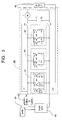
- the device-under-test (DUT) power supply of the present invention is adaptable for use by automatic test equipment, generally designated 10.
- the power supply implements on-tester load circuitry 36 ( Figures 2 and 3) to minimize calibration and validation process times. By providing on-tester load circuitry available to the DUT power supply, costly hardware modifications for calibration/validation procedures are avoided.
- the automatic test equipment or ATE generally includes a computer workstation 12 that couples to a test head 14 via a cable bundle 16.
- the test head houses a plurality of channel cards (not shown) and power supply boards 30 (only one board shown) in relative close proximity to the DUT 40.
- the DUT mounts to a production device-interface-board (DIB) 18, that interfaces with the test head via a tester interface (not shown).
- DIB production device-interface-board
- the tester interface provides an interconnection of signal, ground and power paths between the ATE and the DUT.
- one specific embodiment of the DUT power supply 30 that employs the internal calibration/validation circuitry of the present invention includes digital circuitry 32, power circuitry 34, internal load circuitry 36 and amplifier circuitry 50.
- the digital circuitry 32 provides a digital-to-analog control interface between the tester and the DUT power supply.
- the power circuitry 34 in one embodiment, takes the form of a low-noise switching DC-DC converter.
- the digital circuitry 32, power circuitry 34 and amplifier circuitry 50 of Figure 2 may be thought of collectively as one embodiment of a power generation circuit 60 (in phantom) for purposes of the present invention.
- a current measurement unit 62 coupled to the power generation circuit is a current measurement unit 62 for providing accurate and precise current output information to the power circuitry to effect proper regulation under varying loads and operating conditions.
- the on-tester load circuitry 36 preferably includes internal calibration circuitry in the form of an active load 70, and internal validation circuitry comprising an AC load 80 and a capacitive load 82.
- the active load includes a plurality of FET transistors FC1 - FCN coupled in parallel. Each transistor is regulated by a control circuit C1 - Cn to maintain consistent and stable operation through varying temperatures and other parameters.
- Switching circuitry in the form of a plurality of switches SW1 - SW5 selectively substitutes the DUT 40 for the active load 70 across the power circuitry output in response to software-driver commands.
- the active load 70, the AC load 80 and the capacitive load 82 are coupled to a NIST-traceable current source I.
- the active load 70 is first calibrated using the NIST-traceable current source I.
- the precise value of the current source is stored in a non-volatile RAM memory 64.
- the precise known current value for example 1.000 amperes, is applied to each FET of the active load in sequence. Voltage measurements are taken, for example at the terminals T1 and T2 (by NIST traceable voltage measuring circuitry, not shown) and combined with the known current in accordance with Ohms Law to determine the precise resistance value for each FET transistor.
- the active load resistances for FETs FC1 - FCN may then be activated individually, or in combination, as calibration loads for the current measurement unit 62.
- voltage measurements may be taken (again, using voltage measurement circuitry, not shown) to determine the output current (using basic Ohms law). This measurement is taken in addition to the readings from the current measurement unit itself. The measured current values are then compared. Calibration offsets and gain factors are then calculated, and stored in a calibration memory (not shown) for future current measurements made by the power supply circuitry during normal device testing.
- This combination of circuitry and process achieves a NIST-traceable calibration of the power supply current measurement unit 62 without having to undock the tester (or test head) from a prober or a handler during its normal operating conditions.
- the AC load 80 and the capacitive load 82 emulate the dynamic load currents presented to the power supply by the activity of the DUT and the bulk capacitance usually present on the DIB to minimize voltage droop by supplying instantaneous current to the DUT.
- the varying load of the DUT can be emulated.
- the ability of the power supply to drive the different load capacitances is verified. Validation procedures are highly desirable prior to placing the tester in a production environment.
- the AC load 80 preferably comprises a set of dynamic loads including resistors R1 - Rn to set current levels and FETs FV1 - FVN that are selectively activated to provide a path from the power supply to the load resistors. By implementing several resistors/FETs in parallel, the current level may be varied.
- the capacitive load 82 includes a plurality of FETs F2V1 - F2VN that selectively switch-in respective capacitors C1 - CN. Use of these two circuits in combination allows the load to emulate a wide range of DUT and DIB test conditions, with a wide range of currents and load impedances.
- the inventor has addressed these potential challenges with a unique modification as described below.
- an ATE power supply 100 comprising two power supply units, power supply A 90 and power supply B 92.
- the supplies may be operated individually or in parallel.
- Respective internal loads 94 and 96 are provided for each supply.
- the loads are similar in construction to the selectively switched AC and capacitive loads described earlier, and warrant no further description.
- both supplies are interconnected to the DUT 40 via separate paths 91, 93 (for power supply A 90) and 95, 97 (for power supply B 92).
- the connections allow driving the paths to the DIB 18 from one power supply (for example, power supply A) and connecting the load 96 associated with the other supply (power supply B) to that supply's path to the DIB.
- the path from the overall combined power supply to the load includes the parasitics from the first supply to the DIB and also the parasitics from the DIB back to the load associated with the second power supply.
- the interconnection parasitics and the ability of the power supply to properly supply power through those parasitics may be verified.
- the calibration and validation loads 70, 80 and 82 ( Figure 3) are deactivated by the switching circuitry SWa-SWe, and the DUT 40 switched into the power supply circuit. At this point, the power supply is ready for device testing, where accurate current measurement capability is critically important.
- in-tester as being within the testhead. While this is considered within the scope of the present invention, the "in-tester loads” may be placed anywhere in the tester, including the mainframe and/or the power supply housing.
Landscapes
- Physics & Mathematics (AREA)
- General Physics & Mathematics (AREA)
- Engineering & Computer Science (AREA)
- General Engineering & Computer Science (AREA)
- Tests Of Electronic Circuits (AREA)
Claims (14)
- Stromversorgungsschaltung (30) zur Verwendung in einem Halbleiterprüfgerät (10) zum Speisen eines Messobjekts bzw. Device-Under-Test (40), wobei die Stromversorgungsschaltung umfasst:Stromerzeugungsschaltung (60) mit einem Ausgang zum Erzeugen von Strom für das Messobjekt (Device-Under-Test);Strommessschaltung (62), undLastschaltung (36), die selektiv an den Stromerzeugungsschaltungsausgang (60) gekoppelt und in der Stromversorgungsschaltung (30) angeordnet ist, um die elektrische Last eines Messobjekts selektiv auf die Stromversorgung zu simulieren und dadurch dem Halbleiterprüfgerät zu erlauben, die Stromerzeugungsschaltung (60) unter Verwendung der Strommessschaltung (62) zu validieren und/oder mithilfe einer externen Referenz, die Strommessschaltung zu kalibrieren.
- Stromversorgungsschaltung nach Anspruch 1, wobei die Lastschaltung (36) Kalibrierschaltung (70) für die Kalibrierung von Strommessschaltung umfasst.
- Stromversorgungsschaltung nach Anspruch 2, wobei die Kalibrierschaltung (70) eine aktive kapazitive Last umfasst.
- Stromversorgungsschaltung nach Anspruch 3, wobei die aktive kapazitive Last eine Mehrheit von FETs (Feldeffekttransistors) umfasst, die parallel angeordnet sind, um selektiv zu kooperieren und veränderlichen Widerstand bereitzustellen.
- Stromversorgungsschaltung nach Anspruch 3, die eine NIST-rückverfolgbare Stromquelle (I) umfasst, die selektiv an die aktive kapazitive Last gekoppelt ist.
- Stromversorgungsschaltung nach einem beliebigen vorhergehenden Anspruch, umfassend:ein Stromversorgungsgehäuse (14);die Stromerzeugungsschaltung (60) und die Lastschaltung (36), die innerhalb des Stromversorgungsgehäuses angeordnet ist.
- Stromversorgungsschaltung nach einem beliebigen vorhergehenden Anspruch, wobei:Die Stromerzeugungsschaltung (60) erste und zweite Stromversorgungseinheiten (90, 92) umfasst, die parallel angeordnet sind und jeweilige Ausgänge haben, wobei jede Stromversorgungseinheit jeweilige Kraft- und Messleitungen aufweist, die an das Messobjekt (Device-Under-Test) gekoppelt sind; unddie Lastschaltung (36) erste und zweite Lastschaltungen (94, 96) umfasst, die den ersten und zweiten Stromversorgungseinheiten entsprechen und jeweils an den Stromversorgungseinheitsausgängen angeordnet sind, wobei die Stromversorgungsschaltung weiter Umschaltschaltung umfasst, die funktionsfähig ist, die Lastschaltung selektiv von der zweiten Stromversorgungseinheit in einen geschlossenen Stromkreis mit der ersten Stromversorgungseinheit und den Kraft- und Messleitungen der ersten und zweiten Stromversorgungseinheiten zu platzieren.
- Ein Leistungsstromkreis nach einem beliebigen vorhergehenden Anspruch, wobei die Lastschaltung (36) weiter eine Validierungsschaltung (80, 82) umfasst, die an die Stromerzeugungsschaltung (60) gekoppelt ist, um den dynamischen Betrieb der Stromerzeugungsschaltung (60) bei einer Last zu validieren.
- Stromversorgung nach Anspruch 8, wobei die Validierungsschaltung Widerstandslastschaltung und kapazitive Lastschaltung umfasst.
- Automatische Prüfeinrichtung (10) zum Prüfen eines Messobjekts, die eine Stromversorgungsschaltung nach einem beliebigen vorhergehenden Anspruch umfasst.
- Automatische Prüfeinrichtung zum Prüfen eines Messobjekts, wobei besagtes Messobjekt auf einer Bauelementplatte angeordnet ist und wobei die automatische Prüfeinrichtung umfasst:eine Computer-Workstation;einen Prüfkopf, der an die Computer-Workstation gekoppelt ist; undeine Messobjektstromversorgung, wobei die Messobjektstromversorgung eine Stromversorgungsschaltung (30) nach einem beliebigen der Ansprüche 1 bis 9 umfasst, die im Prüfkopf angeordnet ist, um Strom für das Messobjekt zu generieren.
- Verfahren zum Kalibrieren einer ATE-Stromversorgungsstrommesseinheit (62) ohne Loskoppeln eines Halbleiterprüfgeräts von einer Bauelement-Handhabungsvorrichtung, wobei die Bauelement-Handhabungsvorrichtung ein Messobjekt montiert, die ATE-Stromversorgungsstrommesseinheit anfänglich an das Messobjekt gekoppelt ist und wobei das Verfahren folgende Schritte umfasst:Selektieren einer Prüflast ("In-Tester") Last mit einer bekannten Impedanz;Ersetzen des Messobjekts mit der Prüflast, sodass die ATE-Stromversorgungsstrommesseinheit (62) an die Prüflast gekoppelt ist;Messen des Stroms von der Stromversorgung zur Prüflast mit der Strommesseinheit;Bestimmen einer zweiten Messung des Stroms durch Erkennen der Spannung über die Prüflast und teilen des Spannungswerts durch die bekannte Impedanz;Vergleichen der ersten und zweiten Messungen, um Offsetstrom zu berechnen; undZuordnen von Kalibrierwerten, um für den berechneten Offsetstrom zu kompensieren.
- Verfahren zum Validieren einer Messobjektstromversorgung ohne Loskoppeln eines Halbleiterprüfgeräts von einer Bauelement-Handhabungsvorrichtung, wobei die Bauelement-Handhabungsvorrichtung ein Messobjekt montiert, die Stromversorgung anfänglich an das Messobjekt gekoppelt ist und wobei das Verfahren folgende Schritte umfasst:Selektieren einer dynamischen Prüflast ("In-Tester" Last) mit veränderlichen dynamischen Lastkennwerten; Ersetzen des Messobjekts mit der Prüflast, sodass die Stromversorgung an die Prüflast gekoppelt ist;Antreiben der dynamischen Prüflast mit der Stromversorgung; undBestätigen, dass die Stromversorgung während des Antriebsschritts innerhalb vorbestimmter Performance-Parameter arbeitete.
- Verfahren nach Anspruch 13 der Validierung einer Messobjektstromversorgung, wobei die Stromversorgung erste und zweite parallel angeordnete Stromversorgungseinheiten umfasst, jede Stromversorgungseinheit schaltbar über jeweilige Kraft- und Messleitungen an das Messobjekt gekoppelt ist und jede Einheit jeweilige erste und zweite dynamische Prüflasten aufweist und wobei das Verfahren folgende Schritte umfasst:Selektieren der ersten Stromversorgungseinheit zum Koppeln an das Messobjekt;Ersetzen der Prüflast, die mit der zweiten Stromversorgung assoziiert ist, mit dem Messobjekt;Antreiben der zweiten Prüflast durch die jeweiligen Kraft- und Messleitungen mit der ersten Stromversorgungseinheit; undBestätigen, dass die erste Stromversorgung während des Antriebsschritts innerhalb vorbestimmter Performance-Parameter arbeitete.
Applications Claiming Priority (3)
| Application Number | Priority Date | Filing Date | Title |
|---|---|---|---|
| US943275 | 1986-12-16 | ||
| US09/943,275 US6504395B1 (en) | 2001-08-30 | 2001-08-30 | Method and apparatus for calibration and validation of high performance DUT power supplies |
| PCT/US2002/027616 WO2003021277A2 (en) | 2001-08-30 | 2002-08-28 | Method and apparatus for calibration and validation of high performance dut power supplies |
Publications (2)
| Publication Number | Publication Date |
|---|---|
| EP1440328A2 EP1440328A2 (de) | 2004-07-28 |
| EP1440328B1 true EP1440328B1 (de) | 2007-04-11 |
Family
ID=25479356
Family Applications (1)
| Application Number | Title | Priority Date | Filing Date |
|---|---|---|---|
| EP02757481A Expired - Lifetime EP1440328B1 (de) | 2001-08-30 | 2002-08-28 | Gerät und verfahren zur eichung und validierung von hochleistungs-stromversorgungen für testgeräte |
Country Status (7)
| Country | Link |
|---|---|
| US (1) | US6504395B1 (de) |
| EP (1) | EP1440328B1 (de) |
| AU (1) | AU2002323496A1 (de) |
| DE (1) | DE60219502T2 (de) |
| MY (1) | MY131035A (de) |
| TW (1) | TWI248516B (de) |
| WO (1) | WO2003021277A2 (de) |
Families Citing this family (24)
| Publication number | Priority date | Publication date | Assignee | Title |
|---|---|---|---|---|
| WO2005006101A2 (en) * | 2003-06-30 | 2005-01-20 | Nupower Semiconductor, Inc. | Programmable calibration circuit for power supply current sensing and droop loss compensation |
| US20050046440A1 (en) * | 2003-08-29 | 2005-03-03 | Alcatel | Fault tolerant vital power supply system |
| US6943518B1 (en) * | 2004-04-20 | 2005-09-13 | Delphi Technologies, Inc. | Technique for calibrating a current control circuit |
| US7358625B2 (en) | 2004-12-14 | 2008-04-15 | Woods Industries, Inc. | Power strip with 12 volt outlet |
| US7675310B2 (en) * | 2006-10-23 | 2010-03-09 | Planet Ate, Inc. | Device under test power supply |
| JP5228447B2 (ja) * | 2006-11-07 | 2013-07-03 | 新日鐵住金株式会社 | 高ヤング率鋼板及びその製造方法 |
| TWI367343B (en) * | 2006-11-27 | 2012-07-01 | Hon Hai Prec Ind Co Ltd | Power voltage testing circuit |
| US7888947B2 (en) * | 2007-11-21 | 2011-02-15 | Teradyne, Inc. | Calibrating automatic test equipment |
| US7999530B2 (en) * | 2008-03-21 | 2011-08-16 | Intersil Americas Inc. | Device under test power supply |
| US8242629B2 (en) * | 2009-02-03 | 2012-08-14 | Transistor Devices, Inc. | Hybrid load systems including a dynamic electronic load and passive resistive load modules |
| US20130120010A1 (en) * | 2011-11-10 | 2013-05-16 | Qualcomm Incorporated | Power Measurement System for Battery Powered Microelectronic Chipsets |
| US9645193B2 (en) | 2012-10-23 | 2017-05-09 | Keithley Instruments, Llc | Impedance source ranging apparatus and method |
| US9429629B1 (en) | 2013-03-11 | 2016-08-30 | Magna-Power Electronics, Inc. | Electronic loads |
| US10345418B2 (en) * | 2015-11-20 | 2019-07-09 | Teradyne, Inc. | Calibration device for automatic test equipment |
| US10002317B1 (en) * | 2017-04-10 | 2018-06-19 | Brady Worldwide, Inc. | Label with graphene layer and system for authentication of label |
| WO2018196986A1 (en) * | 2017-04-27 | 2018-11-01 | Advantest Corporation | Calibration arrangement and method for deriving a resistance of a resistor |
| AT520623A1 (de) * | 2017-10-25 | 2019-05-15 | Seibt Kristl & Co Gmbh | Vorrichtung zum Kalibrieren eines Batteriesimulators |
| US10481193B2 (en) * | 2018-02-02 | 2019-11-19 | Texas Instruments Incorporated | Programmable load transient circuit |
| US11243244B2 (en) * | 2019-10-10 | 2022-02-08 | Infineon Technologies Ag | Switched bypass capacitor for component characterization |
| US11221365B2 (en) | 2020-03-11 | 2022-01-11 | Teradyne, Inc. | Calibrating an interface board |
| CN113590390B (zh) * | 2020-04-30 | 2024-12-27 | 鸿富锦精密电子(郑州)有限公司 | 动态智能测试方法、系统、计算机装置及存储介质 |
| US11971434B2 (en) * | 2021-04-30 | 2024-04-30 | Keithley Instruments, Llc | Power source with error detection |
| US12535518B2 (en) | 2022-12-08 | 2026-01-27 | Wolfspeed, Inc. | Multiple transport level tester system |
| CN116299023B (zh) * | 2023-02-10 | 2025-09-02 | 浪潮商用机器有限公司 | 一种电源测试方法、装置、设备及存储介质 |
Family Cites Families (9)
| Publication number | Priority date | Publication date | Assignee | Title |
|---|---|---|---|---|
| JPH0743430A (ja) * | 1993-07-28 | 1995-02-14 | Ando Electric Co Ltd | Icテスタ用校正装置 |
| US5710701A (en) * | 1995-07-31 | 1998-01-20 | Deli Usa, L.P. | Method and apparatus for power supply testing |
| US5773990A (en) * | 1995-09-29 | 1998-06-30 | Megatest Corporation | Integrated circuit test power supply |
| US5917331A (en) * | 1995-10-23 | 1999-06-29 | Megatest Corporation | Integrated circuit test method and structure |
| US5918198A (en) * | 1996-10-22 | 1999-06-29 | Schlumberger Technologies Inc. | Generating pulses in analog channel of ATE tester |
| US6087843A (en) * | 1997-07-14 | 2000-07-11 | Credence Systems Corporation | Integrated circuit tester with test head including regulating capacitor |
| JP3508489B2 (ja) * | 1997-07-29 | 2004-03-22 | 安藤電気株式会社 | プログラマブル比較器のキャリブレーション装置 |
| US6329831B1 (en) * | 1997-08-08 | 2001-12-11 | Advanced Micro Devices, Inc. | Method and apparatus for reliability testing of integrated circuit structures and devices |
| US6339338B1 (en) * | 2000-01-18 | 2002-01-15 | Formfactor, Inc. | Apparatus for reducing power supply noise in an integrated circuit |
-
2001
- 2001-08-30 US US09/943,275 patent/US6504395B1/en not_active Expired - Lifetime
-
2002
- 2002-08-28 EP EP02757481A patent/EP1440328B1/de not_active Expired - Lifetime
- 2002-08-28 WO PCT/US2002/027616 patent/WO2003021277A2/en not_active Ceased
- 2002-08-28 AU AU2002323496A patent/AU2002323496A1/en not_active Abandoned
- 2002-08-28 DE DE60219502T patent/DE60219502T2/de not_active Expired - Fee Related
- 2002-08-30 TW TW091119766A patent/TWI248516B/zh not_active IP Right Cessation
- 2002-08-30 MY MYPI20023244A patent/MY131035A/en unknown
Also Published As
| Publication number | Publication date |
|---|---|
| EP1440328A2 (de) | 2004-07-28 |
| DE60219502T2 (de) | 2008-01-03 |
| WO2003021277A2 (en) | 2003-03-13 |
| WO2003021277A3 (en) | 2003-07-10 |
| DE60219502D1 (de) | 2007-05-24 |
| US6504395B1 (en) | 2003-01-07 |
| AU2002323496A1 (en) | 2003-03-18 |
| TWI248516B (en) | 2006-02-01 |
| MY131035A (en) | 2007-07-31 |
Similar Documents
| Publication | Publication Date | Title |
|---|---|---|
| EP1440328B1 (de) | Gerät und verfahren zur eichung und validierung von hochleistungs-stromversorgungen für testgeräte | |
| US7714603B2 (en) | Predictive, adaptive power supply for an integrated circuit under test | |
| JP4106197B2 (ja) | 半導体テストシステム | |
| US6804620B1 (en) | Calibration method for system performance validation of automatic test equipment | |
| US9939490B2 (en) | Systems and methods mitigating temperature dependence of circuitry in electronic devices | |
| WO2014197208A1 (en) | Calibration device | |
| KR100916762B1 (ko) | 반도체 디바이스 테스트 시스템 | |
| US5875198A (en) | Semiconductor device testing apparatus | |
| US10761130B1 (en) | Voltage driver circuit calibration | |
| US11187745B2 (en) | Stabilizing a voltage at a device under test | |
| JP2000009792A (ja) | テストバーンインシステム、及びテストバーンインシステム校正方法 | |
| KR100483669B1 (ko) | 반도체 집적회로장치를 검사하는 반도체 검사시스템 및 이를 이용한 반도체 검사방법 | |
| US7489123B2 (en) | Calibration control for pin electronics of automatic testing equipment | |
| KR101257246B1 (ko) | 핀 일렉트로닉스 드라이버 | |
| US20040220762A1 (en) | On-site, in-situ application calibration service | |
| KR20080089348A (ko) | 캘리브레이션 회로 | |
| US6703854B2 (en) | Burn-in apparatus having average voltage calculating circuit | |
| KR100916763B1 (ko) | 반도체 디바이스 테스트 시스템 | |
| JP5135611B2 (ja) | テスト装置 | |
| KR20220169901A (ko) | Ic소켓 검사용 다중채널 측정 시스템 및 그 다중채널 측정방법 | |
| KR20020045508A (ko) | 집적회로 테스터 조정방법 및 장치 |
Legal Events
| Date | Code | Title | Description |
|---|---|---|---|
| PUAI | Public reference made under article 153(3) epc to a published international application that has entered the european phase |
Free format text: ORIGINAL CODE: 0009012 |
|
| 17P | Request for examination filed |
Effective date: 20040326 |
|
| AK | Designated contracting states |
Kind code of ref document: A2 Designated state(s): AT BE BG CH CY CZ DE DK EE ES FI FR GB GR IE IT LI LU MC NL PT SE SK TR |
|
| AX | Request for extension of the european patent |
Extension state: AL LT LV MK RO SI |
|
| RIC1 | Information provided on ipc code assigned before grant |
Ipc: G01R 35/00 20060101AFI20060831BHEP Ipc: G01R 31/319 20060101ALI20060831BHEP |
|
| GRAP | Despatch of communication of intention to grant a patent |
Free format text: ORIGINAL CODE: EPIDOSNIGR1 |
|
| RBV | Designated contracting states (corrected) |
Designated state(s): DE FR GB IE IT |
|
| GRAS | Grant fee paid |
Free format text: ORIGINAL CODE: EPIDOSNIGR3 |
|
| GRAA | (expected) grant |
Free format text: ORIGINAL CODE: 0009210 |
|
| AK | Designated contracting states |
Kind code of ref document: B1 Designated state(s): DE FR GB IE IT |
|
| REG | Reference to a national code |
Ref country code: GB Ref legal event code: FG4D |
|
| REG | Reference to a national code |
Ref country code: IE Ref legal event code: FG4D |
|
| REF | Corresponds to: |
Ref document number: 60219502 Country of ref document: DE Date of ref document: 20070524 Kind code of ref document: P |
|
| ET | Fr: translation filed | ||
| PGFP | Annual fee paid to national office [announced via postgrant information from national office to epo] |
Ref country code: DE Payment date: 20071001 Year of fee payment: 6 Ref country code: IT Payment date: 20070828 Year of fee payment: 6 |
|
| PLBE | No opposition filed within time limit |
Free format text: ORIGINAL CODE: 0009261 |
|
| STAA | Information on the status of an ep patent application or granted ep patent |
Free format text: STATUS: NO OPPOSITION FILED WITHIN TIME LIMIT |
|
| 26N | No opposition filed |
Effective date: 20080114 |
|
| GBPC | Gb: european patent ceased through non-payment of renewal fee |
Effective date: 20070828 |
|
| PGFP | Annual fee paid to national office [announced via postgrant information from national office to epo] |
Ref country code: FR Payment date: 20070817 Year of fee payment: 6 |
|
| PG25 | Lapsed in a contracting state [announced via postgrant information from national office to epo] |
Ref country code: IE Free format text: LAPSE BECAUSE OF NON-PAYMENT OF DUE FEES Effective date: 20070828 |
|
| PG25 | Lapsed in a contracting state [announced via postgrant information from national office to epo] |
Ref country code: GB Free format text: LAPSE BECAUSE OF NON-PAYMENT OF DUE FEES Effective date: 20070828 |
|
| REG | Reference to a national code |
Ref country code: FR Ref legal event code: ST Effective date: 20090430 |
|
| PG25 | Lapsed in a contracting state [announced via postgrant information from national office to epo] |
Ref country code: DE Free format text: LAPSE BECAUSE OF NON-PAYMENT OF DUE FEES Effective date: 20090303 Ref country code: IT Free format text: LAPSE BECAUSE OF NON-PAYMENT OF DUE FEES Effective date: 20080828 Ref country code: FR Free format text: LAPSE BECAUSE OF NON-PAYMENT OF DUE FEES Effective date: 20080901 |