EP1438787B1 - Baw-resonator - Google Patents
Baw-resonator Download PDFInfo
- Publication number
- EP1438787B1 EP1438787B1 EP02762340A EP02762340A EP1438787B1 EP 1438787 B1 EP1438787 B1 EP 1438787B1 EP 02762340 A EP02762340 A EP 02762340A EP 02762340 A EP02762340 A EP 02762340A EP 1438787 B1 EP1438787 B1 EP 1438787B1
- Authority
- EP
- European Patent Office
- Prior art keywords
- electrode
- piezoelectric layer
- piezoelectric
- baw
- layers
- Prior art date
- Legal status (The legal status is an assumption and is not a legal conclusion. Google has not performed a legal analysis and makes no representation as to the accuracy of the status listed.)
- Expired - Lifetime
Links
- 239000000463 material Substances 0.000 claims description 24
- 239000000758 substrate Substances 0.000 claims description 20
- 230000005684 electric field Effects 0.000 claims description 14
- 238000004519 manufacturing process Methods 0.000 claims description 2
- 230000010287 polarization Effects 0.000 description 12
- 239000012528 membrane Substances 0.000 description 8
- 239000010409 thin film Substances 0.000 description 7
- 238000006243 chemical reaction Methods 0.000 description 6
- 238000001465 metallisation Methods 0.000 description 5
- 239000004020 conductor Substances 0.000 description 4
- HFGPZNIAWCZYJU-UHFFFAOYSA-N lead zirconate titanate Chemical compound [O-2].[O-2].[O-2].[O-2].[O-2].[Ti+4].[Zr+4].[Pb+2] HFGPZNIAWCZYJU-UHFFFAOYSA-N 0.000 description 4
- 229910052751 metal Inorganic materials 0.000 description 4
- 239000002184 metal Substances 0.000 description 4
- 238000000034 method Methods 0.000 description 4
- 239000013078 crystal Substances 0.000 description 3
- 238000000151 deposition Methods 0.000 description 3
- 230000008021 deposition Effects 0.000 description 3
- 230000000694 effects Effects 0.000 description 3
- 238000001914 filtration Methods 0.000 description 3
- 230000008878 coupling Effects 0.000 description 2
- 238000010168 coupling process Methods 0.000 description 2
- 238000005859 coupling reaction Methods 0.000 description 2
- 239000011810 insulating material Substances 0.000 description 2
- 230000003071 parasitic effect Effects 0.000 description 2
- 230000003542 behavioural effect Effects 0.000 description 1
- 239000003990 capacitor Substances 0.000 description 1
- 239000000919 ceramic Substances 0.000 description 1
- 238000011161 development Methods 0.000 description 1
- 230000018109 developmental process Effects 0.000 description 1
- 238000009826 distribution Methods 0.000 description 1
- 238000005516 engineering process Methods 0.000 description 1
- 239000010408 film Substances 0.000 description 1
- 239000010453 quartz Substances 0.000 description 1
- 230000002336 repolarization Effects 0.000 description 1
- VYPSYNLAJGMNEJ-UHFFFAOYSA-N silicon dioxide Inorganic materials O=[Si]=O VYPSYNLAJGMNEJ-UHFFFAOYSA-N 0.000 description 1
- 239000007787 solid Substances 0.000 description 1
- 238000010897 surface acoustic wave method Methods 0.000 description 1
Images


Classifications
-
- H—ELECTRICITY
- H03—ELECTRONIC CIRCUITRY
- H03H—IMPEDANCE NETWORKS, e.g. RESONANT CIRCUITS; RESONATORS
- H03H9/00—Networks comprising electromechanical or electro-acoustic elements; Electromechanical resonators
- H03H9/46—Filters
- H03H9/54—Filters comprising resonators of piezoelectric or electrostrictive material
- H03H9/58—Multiple crystal filters
- H03H9/582—Multiple crystal filters implemented with thin-film techniques
- H03H9/583—Multiple crystal filters implemented with thin-film techniques comprising a plurality of piezoelectric layers acoustically coupled
-
- H—ELECTRICITY
- H03—ELECTRONIC CIRCUITRY
- H03H—IMPEDANCE NETWORKS, e.g. RESONANT CIRCUITS; RESONATORS
- H03H9/00—Networks comprising electromechanical or electro-acoustic elements; Electromechanical resonators
- H03H9/0023—Networks for transforming balanced signals into unbalanced signals and vice versa, e.g. baluns, or networks having balanced input and output
- H03H9/0095—Networks for transforming balanced signals into unbalanced signals and vice versa, e.g. baluns, or networks having balanced input and output using bulk acoustic wave devices
-
- H—ELECTRICITY
- H03—ELECTRONIC CIRCUITRY
- H03H—IMPEDANCE NETWORKS, e.g. RESONANT CIRCUITS; RESONATORS
- H03H9/00—Networks comprising electromechanical or electro-acoustic elements; Electromechanical resonators
- H03H9/02—Details
- H03H9/02007—Details of bulk acoustic wave devices
- H03H9/02015—Characteristics of piezoelectric layers, e.g. cutting angles
-
- H—ELECTRICITY
- H03—ELECTRONIC CIRCUITRY
- H03H—IMPEDANCE NETWORKS, e.g. RESONANT CIRCUITS; RESONATORS
- H03H9/00—Networks comprising electromechanical or electro-acoustic elements; Electromechanical resonators
- H03H9/15—Constructional features of resonators consisting of piezoelectric or electrostrictive material
- H03H9/17—Constructional features of resonators consisting of piezoelectric or electrostrictive material having a single resonator
- H03H9/171—Constructional features of resonators consisting of piezoelectric or electrostrictive material having a single resonator implemented with thin-film techniques, i.e. of the film bulk acoustic resonator [FBAR] type
- H03H9/172—Means for mounting on a substrate, i.e. means constituting the material interface confining the waves to a volume
- H03H9/174—Membranes
-
- H—ELECTRICITY
- H03—ELECTRONIC CIRCUITRY
- H03H—IMPEDANCE NETWORKS, e.g. RESONANT CIRCUITS; RESONATORS
- H03H9/00—Networks comprising electromechanical or electro-acoustic elements; Electromechanical resonators
- H03H9/15—Constructional features of resonators consisting of piezoelectric or electrostrictive material
- H03H9/17—Constructional features of resonators consisting of piezoelectric or electrostrictive material having a single resonator
- H03H9/171—Constructional features of resonators consisting of piezoelectric or electrostrictive material having a single resonator implemented with thin-film techniques, i.e. of the film bulk acoustic resonator [FBAR] type
- H03H9/172—Means for mounting on a substrate, i.e. means constituting the material interface confining the waves to a volume
- H03H9/175—Acoustic mirrors
-
- H—ELECTRICITY
- H03—ELECTRONIC CIRCUITRY
- H03H—IMPEDANCE NETWORKS, e.g. RESONANT CIRCUITS; RESONATORS
- H03H9/00—Networks comprising electromechanical or electro-acoustic elements; Electromechanical resonators
- H03H9/15—Constructional features of resonators consisting of piezoelectric or electrostrictive material
- H03H9/17—Constructional features of resonators consisting of piezoelectric or electrostrictive material having a single resonator
- H03H9/176—Constructional features of resonators consisting of piezoelectric or electrostrictive material having a single resonator consisting of ceramic material
-
- H—ELECTRICITY
- H03—ELECTRONIC CIRCUITRY
- H03H—IMPEDANCE NETWORKS, e.g. RESONANT CIRCUITS; RESONATORS
- H03H9/00—Networks comprising electromechanical or electro-acoustic elements; Electromechanical resonators
- H03H9/15—Constructional features of resonators consisting of piezoelectric or electrostrictive material
- H03H9/17—Constructional features of resonators consisting of piezoelectric or electrostrictive material having a single resonator
- H03H9/178—Constructional features of resonators consisting of piezoelectric or electrostrictive material having a single resonator of a laminated structure of multiple piezoelectric layers with inner electrodes
-
- H—ELECTRICITY
- H03—ELECTRONIC CIRCUITRY
- H03H—IMPEDANCE NETWORKS, e.g. RESONANT CIRCUITS; RESONATORS
- H03H9/00—Networks comprising electromechanical or electro-acoustic elements; Electromechanical resonators
- H03H9/46—Filters
- H03H9/54—Filters comprising resonators of piezoelectric or electrostrictive material
- H03H9/58—Multiple crystal filters
- H03H9/581—Multiple crystal filters comprising ceramic piezoelectric layers
-
- Y—GENERAL TAGGING OF NEW TECHNOLOGICAL DEVELOPMENTS; GENERAL TAGGING OF CROSS-SECTIONAL TECHNOLOGIES SPANNING OVER SEVERAL SECTIONS OF THE IPC; TECHNICAL SUBJECTS COVERED BY FORMER USPC CROSS-REFERENCE ART COLLECTIONS [XRACs] AND DIGESTS
- Y10—TECHNICAL SUBJECTS COVERED BY FORMER USPC
- Y10T—TECHNICAL SUBJECTS COVERED BY FORMER US CLASSIFICATION
- Y10T29/00—Metal working
- Y10T29/42—Piezoelectric device making
Definitions
- BAW filters comprising one or more BAW resonators, For example, in an interconnection of Ladder type, are in Known in the art.
- the ones used for these BAW filters BAW resonators are so-called thin-film BAW resonators, d. h., resonators that have a piezoelectric Thin film include.
- the disadvantage of these known BAW filters is that no filter topology is known which a signal conversion from unbalanced / balanced (unbalanced / balanced) Signals to balanced / unbalanced (balanced / unbalanced) signals without any restrictions with respect to the common mode load impedance Mass occur or without additional coils or Transformers / converters get along.
- Another disadvantage of these known BAW filter consists in that these are at frequencies greater than 5 GHz piezoelectric layers whose thickness is for a fundamental mode wave (Fundamental mode BAW) are extremely thin ( ⁇ 300 nm).
- Another Disadvantage is that at such frequencies of more than 5 GHz, the resonators having a predetermined impedance level are smaller than this for behavioral reasons (Performance) is desired, since here, for example a poor ratio of area to perimeter of the arrangement which gives rise to strong parasitic effects leads.
- the prior art also includes stacked crystal resonator structures known.
- the present invention is based on the knowledge that the aforementioned disadvantages in known BAW filters or known BAW resonators are thereby avoided can be that the BAW resonators piezoelectric Layers or sections in a piezoelectric material have, their orientations opposite to each other (inverted aligned). This can be on the one hand the range of possible applications of such BAW resonators increase, and there will be an increase in the available Frequency ranges for the use of such BAW resonators allows.
- k mat defines the amplitude and the sign of the voltage for a given electric field and vice versa.
- k mat is directly related to the properties within the (mono- or poly-) crystalline structure of the thin film, such as. B. the preferred orientation, the purity and the grain size of the material used.
- Widely used materials for piezoelectric thin films are z. AlN or ZnO 2 , which may be deposited in a manner which results in polycrystalline layers having a preferred c-axis orientation of the columnar grains, ie orientation.
- the deposition conditions and growth conditions determine whether the c-axis is up-directed, or whether it is down-facing, as described by JA Ruffner. et al., in "Effect of substrate composition on the piezoelectric response of reactively sputtered AlN thin films" in Thin Solid Films 354, 1999, pages 256-261.
- piezoelectric piezoelectric
- B. PZT lead zirconium titanate
- Alignment orientation
- polarization by a polarization process set following the deposition. in this connection becomes a high electric field at elevated temperatures the material is created.
- the orientation of the material of the piezoelectric layer causes the layer when applying an electrical Field in a first direction, the direction of orientation corresponds, contracts, and concerns an electrical Field in a second direction, that of the direction Orientation is opposite, expanding.
- Such a BAW resonator consisting of two layers piezoelectric Material between electrode layers is known from EP-A-0 609 555.
- the present invention is the The object of the invention is to provide an improved BAW resonator, which is a unbalanced input signal into a balanced output signal below Use of such a BAW resonator converts.
- Fig. 1A shows a non-claimed BAW resonator.
- the BAW resonator includes a substrate 100 having a first major surface 102, on which a first connection electrode 104 from a metal or other conductive material is.
- a first connection electrode 104 from a metal or other conductive material is.
- a first piezoelectric Layer 106 disposed on the turn a second piezoelectric Layer 108 is arranged.
- a second electrode 110 made of a metal or another conductive material.
- the first electrode 104 is, for example, an input electrode
- the second electrode 110 is, for example, an output electrode.
- the substrate 100 comprises a recess 112, to form a membrane region 114 on which the BAW resonator is formed to an acoustic decoupling of Resonator of underlying elements or layers to enable.
- the decoupling by a so-called acoustic reflector can be achieved, then disposed between the substrate 100 and the electrode 104 would. Both the decoupling by means of a membrane as well the decoupling using an acoustic reflector are known in the art.
- the first piezoelectric layer 106 has been grown in such a way that the orientation of the material in the same direction takes place in the direction of the arrows shown in FIG. 1A in the layer 106, ie the layer 106 is polarized in this direction.
- the second layer 108 has been formed such that the orientation of the material in this layer, that is the polarization of this material, is in a direction opposite to the polarization in layer 106, as indicated by the opposite arrows in the layer 108 in FIG 1A can be seen.
- the polarization of the layers can also be achieved after application of the same by application of a suitable electric field.
- the piezoelectric layers 106 and 108 are made of, for example, PZT material (lead zirconium titanate). Otherwise, the layers are made of, for example, AlN or ZnO 2 .
- Fig. 1B is another not claimed BAW resonator shown which differs from the described thereby with reference to FIG. 1A differentiates that instead of the two separate piezoelectric Layers 106 and 108 a piezoelectric material 116 is disposed between the electrodes 104 and 110. It Thus, only one piezoelectric layer 116 is provided. However, the layer 116 is made to have a first section 106 and a second section 108, in which the material of the piezoelectric layer 116 has an orientation or orientation (polarization), which is opposite to each other, as by the Arrows is shown. The different sections are separated by the dashed line in Fig. 1B.
- the layer 116 shown in Fig. 1B is so made that initially the first section 106 grown becomes, using process parameters which the enable alignment shown there. Then it will open the thus generated portion 106 of the second section 108 below
- the piezoelectric layer 116 is made of AlN or ZnO 2 .
- the layer 116 may also be made of a ferroelectric material in which polarization is induced using the application of an electric field, in which connection it must be ensured that after deposition of the first portion or layer 106 and polarization thereof the application of another electric field to the overall structure to polarize the layer 108 does not cause repolarization of the portion 106.
- the piezoelectric layers are arranged such that the same are acoustically coupled together.
- the Layers may be contiguous or spaced apart be arranged, in the latter case a or more layers between them can.
- Fig. 2A shows an unstressed high frequency resonator with a 1-port
- the N 4 piezoelectric layers includes with alternating orientation.
- a reflector layer 118 is formed, in the an acoustic mirror or acoustic reflector 120 is arranged, which has a plurality of individual layers 120a to 120c, which alternately a high acoustic.
- Impedance and a low acoustic impedance include.
- the acoustic reflector 120 By the acoustic reflector 120 is arranged above it BAW resonator acoustically decoupled from the substrate.
- the described reflector 120 is known in the art is known, and is therefore not explained in detail.
- the reflector layer 118 is at least partially the first (lower) electrode 104 formed via a wire 128 with a connection 130 is connectable.
- the areas of the main surface 124 of the reflector layer 118, not by the first electrode 104 are covered by an insulating Layer 132 covered.
- the first piezoelectric layer 106 is on the electrode 104 and on a portion of the insulating layer 132 arranged.
- the second piezoelectric layer 108 is arranged, on the turn another piezoelectric Layer 134 and another second piezoelectric layer 136 is arranged.
- Fig. 2A see Figs Arrows in the respective piezoelectric layers
- the second (upper) electrode 110 is arranged, which via a Wire 138 is connectable to a terminal 140.
- the BAW resonator according to FIG. 2A is formed in the area where the lower Electrode 104 and upper electrode 110 overlap, and also over this area, the layers 120a extend to 120c of the acoustic mirror or reflector 120.
- the stacked layer structure of piezoelectric shown in Fig. 2A Layers that have alternating orientations, is especially for high volume acoustic waves Frequencies advantageous.
- Resonator can be between each piezoelectric layers 106, 108, 134, 136 additional Metal layers or other intermediate layers provided However, it is not mandatory to do this Layers for the operation of the same as a resonator electrically connect to.
- the element shown in Fig. 2A has strong series resonances and parallel resonances at frequencies which half the acoustic wavelength in each of the piezoelectric Layer correspond.
- the stack of piezoelectric Layers between the two electrodes 104 and 110 works in overmode mode. The electric field has through the entire stack the same orientation, the changing Orientations of the material, however, ensure that the coupling to this overmode is the strongest compared with every other mode at a lower or a higher level Frequency.
- the standing wave 142 is shown, which is in the stack of piezoelectric layers 106, 108, 134, 136 established.
- the course is the electric fields and the sign of the same indicated.
- N the number of piezoelectric layers
- the element by the acoustic To isolate mirror 120 from substrate may be the same also be arranged on a membrane region (see Fig. 1).
- Fig. 2A which is the acoustic Mirror 120 used is that these acoustic mirrors 120 are easy to manufacture, and at higher frequencies have increased robustness.
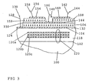
- FIG. 3 Based on the Fig. 3 below, a first embodiment described, which one Conversion from symmetric / unbalanced to unbalanced / symmetric Signals possible.
- elements which have already been described with reference to FIGS. 1 and 2, and have the same or similar effect with the provided the same reference numerals.
- the first (lower) electrode 104 is partially formed, the portion of the surface 124 that is not through the electrode 104 of a metal or a conductive Material is formed by an insulating material 132 is covered.
- the first piezoelectric layer 106 is on a portion of the lower electrode 104 as well as on a Section of the insulating layer 132 is arranged.
- a third electrode 144 disposed via a wire 146 having a reference potential 148, z. B. mass, is connectable. Those Sections of the substrate 100 facing away from the surface first piezoelectric layer 106, not by the third electrode 144 are covered by an insulating Material 150 covered.
- the second piezoelectric layer 108 is on the the first piezoelectric layer 106 is arranged to be the same covers a part of the same, wherein the second piezoelectric Layer 108 at least partially on the third Electrode 144 is arranged.
- Distanced from the second piezoelectric layer 108 is another first piezoelectric Layer 152 on the first piezoelectric Layer 106, wherein the further first piezoelectric Layer 152 at least partially on the third electrode 144 is arranged.
- the second piezoelectric layer 108 and the further first piezoelectric layer 152 are in the embodiment shown in Fig. 3 in such a way on the third electrode 144 and spaced from each other, that the wire 146 between the second piezoelectric Layer 108 and the other first piezoelectric Layer 152 is connected to the third electrode.
- first piezoelectric layer 152 On the further first piezoelectric layer 152 is at least partially disposed a fourth electrode 154, the is connectable via a wire 156 to a terminal 158. Likewise, on the second piezoelectric layer 108 is a fifth electrode 160 which, via a wire 162 with a connection 164 is connectable.
- Fig. 3 By the arrangement shown in Fig. 3 is actually a Pair formed by stacked layers, wherein the in Fig. 3 right-lying portion of the element piezoelectric Layers with opposite orientation (polarization) and piezoelectric in the region on the left in FIG. 3 Has layers with the same orientation (polarization).
- terminal 130 is an input terminal, and are the terminals 158 and 164 two output terminals, so leads the in Fig. 3 structure shown a conversion of unbalanced Signals to symmetric signals through, and further is a Filtering performed. If the terminal 130 is output terminal, and the terminals 158 and 164 are input terminals, so the structure shown next to the filtering leads nor a conversion from balanced signals to unbalanced ones Through signals.
- FIG. 1 which includes a pair of stacked resonators, has a common center electrode 144 (ground) and a common outer electrode 104.
- the piezoelectric layer below one of the remaining electrodes has an inverted orientation (polarization) compared to the other piezoelectric layers ) and thus generates a signal with an inverted sign at this output.
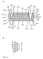
- FIG. 4 is another Embodiment of the present invention explained, wherein also already described here with reference to the preceding figures Elements that have the same or similar effect have the same reference numerals and not described again become.
- FIG. 4A shows a resonator for low frequencies.
- the N 4 piezoelectric layers with alternating orientation (Polarization).
- the Resonator device here using the membrane approach " (see Fig. 1) realized.
- the membrane 114 comprises the insulating portions 132 and the lower or first Electrode 104, on which the first piezoelectric layer 106 is formed.
- a second electrode 166 formed, and the remaining portions the substrate 100 facing away from the surface of the piezoelectric Layer 106 are through an insulating layer 168 covered.
- a third electrode 170 at least partially formed is on the exposed surface turn a third electrode 170 at least partially formed is.
- the remaining areas of the exposed surface the second piezoelectric layer 108 are provided with an insulating Layer 172 covered.
- On the third electrode 170 and the insulating layer 172 is another first piezoelectric Layer 134 formed on the turn in part a fourth electrode 174 is formed.
- another second piezoelectric layer 136 is formed, on the exposed surface at least partially a fifth electrode is formed.
- the first electrode 104, the third electrode 170, and the fifth electrode 178 formed so that they overlap, creating a first electrode group is formed.
- the second electrode 168 and the fourth electrode 174 are also arranged overlapping, and form a second electrode group.
- the first Electrode group and the second electrode group is only partially overlapping, so that the in 4A show areas without conductive material.
- trenches 182 and 184 are formed, one each Metallization 186 and 188 have.
- the trenches 182 and 184 are formed such that the metallizations disposed therein 186 and 188 with the first electrode group (electrodes 104, 172, 178) or the second electrode group (electrodes 166, 174) are connected, as in Fig. 4A to recognize.
- the first metallization 186 is connected via a wire 190 to a Connection 192 connected.
- the second metallization 188 connected via a wire 194 with a port 196.
- the BAW resonator shown in FIG. 4A is optimized to provide the Size of the resonator for applications at lower frequencies or to extremely low impedance levels gain.
- a stack of some piezoelectric Layers with alternating orientation and provided Intermediate electrodes are resonant in the fundamental mode or basic mode. This is achieved by that alternating electric fields to the piezoelectric Layers are created, resulting in a uniform Voltage sign in the entire stack leads.
- electrical Seen N capacitors exist in parallel which means that either the surface of the resonator by a factor of N or one compared to conventional resonators constant area, the impedance around a factor N is reduced.
- Fig. 4B lie the electric fields due to the configuration with the intermediate electrodes alternating so that there is an equal sign of tension through the entire stack results. It is pointed out that the thickness of the piezoelectric layers and Electrodes are not necessarily identical for all n layers have to be. With regard to the desired resonator bandwidth There may not exist an optimal solution same thickness requires, which further the setting of Voltage distribution in the acoustic stack allows. Instead of the realization shown in Fig. 4A by means of "Membrane approach" can also be described with reference to FIG. 2 or 3 Realization using the acoustic reflector be used.
- connection surfaces described above are led out Sections of the associated electrodes.
- the connection surfaces have an area that is sufficient to hold the wire to it to fix.
- the BAW resonators can For example, in flip-chip technology with associated contact surfaces get connected. Others, in the art Known connection methods can also be used become.
- Housing may be provided to complete the BAW resonator include.
- this is achieved in that in the BAW resonator covering section another acoustic reflector is provided.
Landscapes
- Physics & Mathematics (AREA)
- Acoustics & Sound (AREA)
- Chemical & Material Sciences (AREA)
- Engineering & Computer Science (AREA)
- Ceramic Engineering (AREA)
- Crystallography & Structural Chemistry (AREA)
- Piezo-Electric Or Mechanical Vibrators, Or Delay Or Filter Circuits (AREA)
Description
- 100
- Substrat
- 102
- erste Hauptoberfläche des Substrats 100
- 104
- erste Elektrode
- 106
- erste piezoelektrische Schicht
- 108
- zweite piezoelektrische Schicht
- 110
- zweite Elektrode
- 112
- Ausnehmung
- 114
- Membranbereich
- 116
- piezoelektrisches Material
- 118
- Reflektorschicht
- 120
- akustischer Reflektor
- 120a-120c
- Reflektorschichten
- 122
- Abschnitt des Reflektors
- 124
- Hauptoberfläche der Reflektorschicht
- 126
- erste Elektrode
- 128
- Draht
- 130
- Anschluss
- 132
- isolierende Schicht
- 134
- weitere erste piezoelektrische Schicht
- 136
- weitere zweite piezoelektrische Schicht
- 138
- Draht
- 140
- Anschluss
- 142
- stehende Welle
- 144
- dritte Elektrode
- 146
- Draht
- 148
- Bezugspotential
- 150
- isolierende Schicht
- 152
- weitere erste piezoelektrische Schicht
- 154
- vierte Elektrode
- 156
- Draht
- 158
- Anschluss
- 160
- fünfte Elektrode
- 162
- Draht
- 164
- Anschluss
- 166
- zweite Elektrode
- 168
- isolierende Schicht
- 170
- dritte Elektrode
- 172
- isolierende Schicht
- 174
- vierte Elektrode
- 176
- isolierende Schicht
- 178
- fünfte Elektrode
- 180
- freiliegender Bereich
- 182,184
- Gräben
- 186,188
- Metallisierungen
- 190
- Draht
- 192
- Anschluss
- 194
- Draht
- 196
- Anschluss
Claims (9)
- BAW-Resonator, mit
einer ersten piezoelektrischen Schicht (106) aus einem Material, das in eine erste Richtung orientiert ist, und einer zweiten piezoelektrischen Schicht (108) aus einem Material, das in einer zweiten Richtung, die der ersten Richtung entgegengesetzt ist, orientiert ist, wobei die erste piezoelektrische Schicht (106) und die zweite piezoelektrische Schicht (108) akustisch miteinander gekoppelt sind,
einer ersten Elektrode (104) auf der die erste piezoelektrische Schicht (106) zumindest teilweise gebildet ist;
einer zweiten Elektrode (144), die zumindest teilweise auf der ersten piezoelektrischen Schicht (106) gebildet ist, wobei die zweite piezoelektrische Schicht (108) zumindest teilweise auf einem ersten Abschnitt der zweiten Elektrode (144) angeordnet ist;
einer weiteren ersten piezoelektrischen Schicht (152) die zumindest teilweise auf einem zweiten Abschnitt der zweiten Elektrode (144) angeordnet ist, wobei die zweite piezoelektrische Schicht (108) und die weitere erste piezoelektrische Schicht (152) voneinander beabstandet angeordnet sind wobei die weitere erste piezoelektrische Schicht dieselbe Orientierung aufweist wie die erste Piezoelektrische Schicht.
einer dritten Elektrode (160), die zumindest teilweise auf der zweiten piezoelektrischen Schicht (108) angeordnet ist; und
einer vierten Elektrode (154), die zumindest teilweise auf der weiteren ersten piezoelektrischen Schicht (152) angeordnet ist. - BAW-Resonator nach Anspruch 1, mit
einem Substrat (100); und
einem akustischen Reflektor (120), auf dem die piezoelektrischen Schichten angeordnet sind, so dass dieselben akustisch von dem Substrat (100) getrennt sind. - BAW-Resonator nach Anspruch 1, mit
einem Substrat (100), das einen Membranbereich (114) aufweist, wobei die piezoelektrischen Schichten auf dem Membranbereich (114) angeordnet sind, so dass dieselben akustisch von dem Substrat (100) getrennt sind. - BAW-Resonator nach Anspruch 2, mit einem weiteren akustischen Reflektor, auf dem die piezoelektrischen Schichten angeordnet ist.
- BAW-Resonator nach einem der Ansprüche 1 bis 4, bei dem die erste Elektrode (104) eine Eingangselektrode, die zweite Elektrode (144) eine Masseelektrode, und die dritte und vierte Elektrode (160, 154) eine erste und zweite Ausgangselektrode sind.
- BAW-Resonator nach einem der Ansprüche 1 bis 4, bei dem die erste Elektrode (104) eine Ausgangselektrode, die zweite Elektrode (144) eine Masseelektrode, und die dritte und vierte Elektrode (160, 154) eine erste und zweite Eingangselektrode sind.
- BAW-Resonator nach einem der Ansprüche 1 bis 6, bei dem die Orientierung der ersten und/oder der zweiten piezoelektrischen Schicht (106, 108) beim Erzeugen derselben durch Einstellen der Aufwachsbedingungen festgelegt ist.
- BAW-Resonator nach einem der Ansprüche 1 bis 7, bei dem die erste und/oder zweite piezoelektrische Schicht (106, 108) aus einem ferroelektrischen Material bestehen, wobei nach dem Erzeugen der piezoelektrischen Schichten durch Anlegen eines geeigneten elektrischen Feldes die Orientierung derselben festgelegt ist.
- BAW-Filter mit einem oder mehreren BAW-Resonatoren nach einem der Ansprüche 1 bis 8.
Applications Claiming Priority (3)
| Application Number | Priority Date | Filing Date | Title |
|---|---|---|---|
| DE10149542A DE10149542A1 (de) | 2001-10-08 | 2001-10-08 | BAW-Resonator |
| DE10149542 | 2001-10-08 | ||
| PCT/EP2002/007700 WO2003032486A1 (de) | 2001-10-08 | 2002-07-10 | Baw-resonator |
Publications (2)
| Publication Number | Publication Date |
|---|---|
| EP1438787A1 EP1438787A1 (de) | 2004-07-21 |
| EP1438787B1 true EP1438787B1 (de) | 2005-03-02 |
Family
ID=7701766
Family Applications (1)
| Application Number | Title | Priority Date | Filing Date |
|---|---|---|---|
| EP02762340A Expired - Lifetime EP1438787B1 (de) | 2001-10-08 | 2002-07-10 | Baw-resonator |
Country Status (4)
| Country | Link |
|---|---|
| US (1) | US6975183B2 (de) |
| EP (1) | EP1438787B1 (de) |
| DE (2) | DE10149542A1 (de) |
| WO (1) | WO2003032486A1 (de) |
Cited By (1)
| Publication number | Priority date | Publication date | Assignee | Title |
|---|---|---|---|---|
| US7515018B2 (en) | 2006-08-31 | 2009-04-07 | Martin Handtmann | Acoustic resonator |
Families Citing this family (126)
| Publication number | Priority date | Publication date | Assignee | Title |
|---|---|---|---|---|
| DE10246791B4 (de) * | 2002-10-08 | 2017-10-19 | Snaptrack, Inc. | Mit akustischen Volumenwellen arbeitender Resonator und Schaltung mit dem Resonator |
| DE10301261B4 (de) * | 2003-01-15 | 2018-03-22 | Snaptrack, Inc. | Mit akustischen Volumenwellen arbeitendes Bauelement und Verfahren zur Herstellung |
| US7275292B2 (en) | 2003-03-07 | 2007-10-02 | Avago Technologies Wireless Ip (Singapore) Pte. Ltd. | Method for fabricating an acoustical resonator on a substrate |
| US6927651B2 (en) * | 2003-05-12 | 2005-08-09 | Agilent Technologies, Inc. | Acoustic resonator devices having multiple resonant frequencies and methods of making the same |
| US7400217B2 (en) | 2003-10-30 | 2008-07-15 | Avago Technologies Wireless Ip Pte Ltd | Decoupled stacked bulk acoustic resonator band-pass filter with controllable pass bandwith |
| EP1528677B1 (de) | 2003-10-30 | 2006-05-10 | Agilent Technologies, Inc. | Akustisch gekoppelter Dünnschicht-Transformator mit zwei piezoelektrischen Elementen, welche entgegengesetzte C-Axen Orientierung besitzten |
| US7332985B2 (en) | 2003-10-30 | 2008-02-19 | Avago Technologies Wireless Ip (Singapore) Pte Ltd. | Cavity-less film bulk acoustic resonator (FBAR) devices |
| US7019605B2 (en) | 2003-10-30 | 2006-03-28 | Larson Iii John D | Stacked bulk acoustic resonator band-pass filter with controllable pass bandwidth |
| US6946928B2 (en) | 2003-10-30 | 2005-09-20 | Agilent Technologies, Inc. | Thin-film acoustically-coupled transformer |
| US7615833B2 (en) | 2004-07-13 | 2009-11-10 | Avago Technologies Wireless Ip (Singapore) Pte. Ltd. | Film bulk acoustic resonator package and method of fabricating same |
| US7388454B2 (en) | 2004-10-01 | 2008-06-17 | Avago Technologies Wireless Ip Pte Ltd | Acoustic resonator performance enhancement using alternating frame structure |
| US8981876B2 (en) | 2004-11-15 | 2015-03-17 | Avago Technologies General Ip (Singapore) Pte. Ltd. | Piezoelectric resonator structures and electrical filters having frame elements |
| US7202560B2 (en) | 2004-12-15 | 2007-04-10 | Avago Technologies Wireless Ip (Singapore) Pte. Ltd. | Wafer bonding of micro-electro mechanical systems to active circuitry |
| US7791434B2 (en) * | 2004-12-22 | 2010-09-07 | Avago Technologies Wireless Ip (Singapore) Pte. Ltd. | Acoustic resonator performance enhancement using selective metal etch and having a trench in the piezoelectric |
| DE102005004435B4 (de) * | 2005-01-31 | 2006-10-19 | Infineon Technologies Ag | Baw-resonator |
| US7427819B2 (en) | 2005-03-04 | 2008-09-23 | Avago Wireless Ip Pte Ltd | Film-bulk acoustic wave resonator with motion plate and method |
| US7369013B2 (en) | 2005-04-06 | 2008-05-06 | Avago Technologies Wireless Ip Pte Ltd | Acoustic resonator performance enhancement using filled recessed region |
| US7436269B2 (en) | 2005-04-18 | 2008-10-14 | Avago Technologies Wireless Ip (Singapore) Pte. Ltd. | Acoustically coupled resonators and method of making the same |
| DE102005028927B4 (de) | 2005-06-22 | 2007-02-15 | Infineon Technologies Ag | BAW-Vorrichtung |
| US7868522B2 (en) | 2005-09-09 | 2011-01-11 | Avago Technologies Wireless Ip (Singapore) Pte. Ltd. | Adjusted frequency temperature coefficient resonator |
| US7391286B2 (en) | 2005-10-06 | 2008-06-24 | Avago Wireless Ip Pte Ltd | Impedance matching and parasitic capacitor resonance of FBAR resonators and coupled filters |
| US7737807B2 (en) | 2005-10-18 | 2010-06-15 | Avago Technologies Wireless Ip (Singapore) Pte. Ltd. | Acoustic galvanic isolator incorporating series-connected decoupled stacked bulk acoustic resonators |
| US7423503B2 (en) | 2005-10-18 | 2008-09-09 | Avago Technologies Wireless Ip (Singapore) Pte. Ltd. | Acoustic galvanic isolator incorporating film acoustically-coupled transformer |
| US7525398B2 (en) | 2005-10-18 | 2009-04-28 | Avago Technologies General Ip (Singapore) Pte. Ltd. | Acoustically communicating data signals across an electrical isolation barrier |
| US7675390B2 (en) | 2005-10-18 | 2010-03-09 | Avago Technologies Wireless Ip (Singapore) Pte. Ltd. | Acoustic galvanic isolator incorporating single decoupled stacked bulk acoustic resonator |
| US7425787B2 (en) * | 2005-10-18 | 2008-09-16 | Avago Technologies Wireless Ip (Singapore) Pte. Ltd. | Acoustic galvanic isolator incorporating single insulated decoupled stacked bulk acoustic resonator with acoustically-resonant electrical insulator |
| US7463499B2 (en) | 2005-10-31 | 2008-12-09 | Avago Technologies General Ip (Singapore) Pte Ltd. | AC-DC power converter |
| US7561009B2 (en) | 2005-11-30 | 2009-07-14 | Avago Technologies General Ip (Singapore) Pte. Ltd. | Film bulk acoustic resonator (FBAR) devices with temperature compensation |
| US7612636B2 (en) | 2006-01-30 | 2009-11-03 | Avago Technologies Wireless Ip (Singapore) Pte. Ltd. | Impedance transforming bulk acoustic wave baluns |
| US7746677B2 (en) | 2006-03-09 | 2010-06-29 | Avago Technologies Wireless Ip (Singapore) Pte. Ltd. | AC-DC converter circuit and power supply |
| US7479685B2 (en) | 2006-03-10 | 2009-01-20 | Avago Technologies General Ip (Singapore) Pte. Ltd. | Electronic device on substrate with cavity and mitigated parasitic leakage path |
| US7629865B2 (en) | 2006-05-31 | 2009-12-08 | Avago Technologies Wireless Ip (Singapore) Pte. Ltd. | Piezoelectric resonator structures and electrical filters |
| JPWO2007145127A1 (ja) * | 2006-06-15 | 2009-10-29 | 宏一 平間 | 複合共振回路 |
| DE102006032950B4 (de) * | 2006-07-17 | 2010-07-22 | Epcos Ag | Schaltung mit BAW-Resonatoren |
| US7508286B2 (en) | 2006-09-28 | 2009-03-24 | Avago Technologies Wireless Ip (Singapore) Pte. Ltd. | HBAR oscillator and method of manufacture |
| US7791435B2 (en) | 2007-09-28 | 2010-09-07 | Avago Technologies Wireless Ip (Singapore) Pte. Ltd. | Single stack coupled resonators having differential output |
| US7855618B2 (en) | 2008-04-30 | 2010-12-21 | Avago Technologies Wireless Ip (Singapore) Pte. Ltd. | Bulk acoustic resonator electrical impedance transformers |
| US7732977B2 (en) | 2008-04-30 | 2010-06-08 | Avago Technologies Wireless Ip (Singapore) | Transceiver circuit for film bulk acoustic resonator (FBAR) transducers |
| EP2237416A1 (de) * | 2009-03-30 | 2010-10-06 | Nxp B.V. | Vorrichtung mit einem elektroakustischen Balun |
| US8248185B2 (en) | 2009-06-24 | 2012-08-21 | Avago Technologies Wireless Ip (Singapore) Pte. Ltd. | Acoustic resonator structure comprising a bridge |
| US8902023B2 (en) | 2009-06-24 | 2014-12-02 | Avago Technologies General Ip (Singapore) Pte. Ltd. | Acoustic resonator structure having an electrode with a cantilevered portion |
| US8193877B2 (en) | 2009-11-30 | 2012-06-05 | Avago Technologies Wireless Ip (Singapore) Pte. Ltd. | Duplexer with negative phase shifting circuit |
| FR2954626B1 (fr) * | 2009-12-23 | 2013-12-06 | Commissariat Energie Atomique | Resonateur acoustique comprenant un electret, et procede de fabrication de ce resonateur, application aux filtres commutables a resonateurs couples |
| US8796904B2 (en) * | 2011-10-31 | 2014-08-05 | Avago Technologies General Ip (Singapore) Pte. Ltd. | Bulk acoustic resonator comprising piezoelectric layer and inverse piezoelectric layer |
| US9243316B2 (en) | 2010-01-22 | 2016-01-26 | Avago Technologies General Ip (Singapore) Pte. Ltd. | Method of fabricating piezoelectric material with selected c-axis orientation |
| JP5754129B2 (ja) * | 2010-03-11 | 2015-07-29 | セイコーエプソン株式会社 | 圧電素子、圧電センサー、電子機器、および圧電素子の製造方法 |
| FI123640B (fi) | 2010-04-23 | 2013-08-30 | Teknologian Tutkimuskeskus Vtt | Laajakaistainen akustisesti kytketty ohutkalvo-BAW-suodin |
| US8962443B2 (en) | 2011-01-31 | 2015-02-24 | Avago Technologies General Ip (Singapore) Pte. Ltd. | Semiconductor device having an airbridge and method of fabricating the same |
| US9425764B2 (en) | 2012-10-25 | 2016-08-23 | Avago Technologies General Ip (Singapore) Pte. Ltd. | Accoustic resonator having composite electrodes with integrated lateral features |
| US9203374B2 (en) | 2011-02-28 | 2015-12-01 | Avago Technologies General Ip (Singapore) Pte. Ltd. | Film bulk acoustic resonator comprising a bridge |
| US9048812B2 (en) | 2011-02-28 | 2015-06-02 | Avago Technologies General Ip (Singapore) Pte. Ltd. | Bulk acoustic wave resonator comprising bridge formed within piezoelectric layer |
| US9148117B2 (en) | 2011-02-28 | 2015-09-29 | Avago Technologies General Ip (Singapore) Pte. Ltd. | Coupled resonator filter comprising a bridge and frame elements |
| US9136818B2 (en) | 2011-02-28 | 2015-09-15 | Avago Technologies General Ip (Singapore) Pte. Ltd. | Stacked acoustic resonator comprising a bridge |
| US9083302B2 (en) | 2011-02-28 | 2015-07-14 | Avago Technologies General Ip (Singapore) Pte. Ltd. | Stacked bulk acoustic resonator comprising a bridge and an acoustic reflector along a perimeter of the resonator |
| US9154112B2 (en) | 2011-02-28 | 2015-10-06 | Avago Technologies General Ip (Singapore) Pte. Ltd. | Coupled resonator filter comprising a bridge |
| US8575820B2 (en) | 2011-03-29 | 2013-11-05 | Avago Technologies General Ip (Singapore) Pte. Ltd. | Stacked bulk acoustic resonator |
| US9444426B2 (en) | 2012-10-25 | 2016-09-13 | Avago Technologies General Ip (Singapore) Pte. Ltd. | Accoustic resonator having integrated lateral feature and temperature compensation feature |
| US8350445B1 (en) | 2011-06-16 | 2013-01-08 | Avago Technologies Wireless Ip (Singapore) Pte. Ltd. | Bulk acoustic resonator comprising non-piezoelectric layer and bridge |
| US9406865B2 (en) | 2011-08-19 | 2016-08-02 | Qualcomm Incorporated | Composite piezoelectric laterally vibrating resonator |
| US8922302B2 (en) | 2011-08-24 | 2014-12-30 | Avago Technologies General Ip (Singapore) Pte. Ltd. | Acoustic resonator formed on a pedestal |
| FR2981203B1 (fr) * | 2011-10-05 | 2013-12-20 | Centre Nat Rech Scient | Transducteur electroacoustique a polarisation ferroelectrique periodique realise sur une structure verticale micro usinee. |
| FR2996080B1 (fr) * | 2012-09-27 | 2016-01-15 | Thales Sa | Dispositif acoustique comprenant un cristal phononique reglable |
| US10079334B2 (en) | 2012-12-21 | 2018-09-18 | Snaptrack, Inc. | BAW component and method for manufacturing a BAW component |
| WO2014094884A1 (en) * | 2012-12-21 | 2014-06-26 | Epcos Ag | Baw component, lamination for a baw component, and method for manufacturing a baw component, said baw component comprising two stacked piezoelectric materials that differ |
| JP6105084B2 (ja) | 2012-12-21 | 2017-03-29 | エプコス アクチエンゲゼルシャフトEpcos Ag | 窒化アルミニウム及びスカンジウムを有したmems部品の製造方法 |
| US9583704B2 (en) * | 2013-01-16 | 2017-02-28 | Helmholtz-Zentrum Dresden-Rossendorf E.V. | Complementary resistance switch, contact-connected polycrystalline piezo- or ferroelectric thin-film layer, method for encrypting a bit sequence |
| US10333494B2 (en) | 2014-12-24 | 2019-06-25 | Qorvo Us, Inc. | Simplified acoustic RF resonator parallel capacitance compensation |
| US9338147B1 (en) * | 2015-04-24 | 2016-05-10 | Extrahop Networks, Inc. | Secure communication secret sharing |
| US9602076B1 (en) * | 2015-05-19 | 2017-03-21 | Qorvo Us, Inc. | Resonators with balancing capacitor |
| DE102016103959A1 (de) * | 2016-03-04 | 2017-09-07 | Snaptrack, Inc. | BAW-Resonator mit reduzierten Störmoden, BAW-Filter und Verfahren zum Herstellen |
| US10432162B2 (en) | 2016-03-31 | 2019-10-01 | Avago Technologies International Sales Pte. Limited | Acoustic resonator including monolithic piezoelectric layer having opposite polarities |
| US20170288121A1 (en) * | 2016-03-31 | 2017-10-05 | Avago Technologies General Ip (Singapore) Pte. Ltd | Acoustic resonator including composite polarity piezoelectric layer having opposite polarities |
| CN107342357B (zh) * | 2016-04-28 | 2022-08-16 | 新科实业有限公司 | 薄膜压电元件及其制造方法 |
| US10581403B2 (en) | 2016-07-11 | 2020-03-03 | Qorvo Us, Inc. | Device having a titanium-alloyed surface |
| US11050412B2 (en) | 2016-09-09 | 2021-06-29 | Qorvo Us, Inc. | Acoustic filter using acoustic coupling |
| US11736088B2 (en) | 2016-11-15 | 2023-08-22 | Global Communication Semiconductors, Llc | Film bulk acoustic resonator with spurious resonance suppression |
| US11165413B2 (en) | 2017-01-30 | 2021-11-02 | Qorvo Us, Inc. | Coupled resonator structure |
| US11165412B2 (en) | 2017-01-30 | 2021-11-02 | Qorvo Us, Inc. | Zero-output coupled resonator filter and related radio frequency filter circuit |
| US10873318B2 (en) | 2017-06-08 | 2020-12-22 | Qorvo Us, Inc. | Filter circuits having acoustic wave resonators in a transversal configuration |
| US20190089331A1 (en) * | 2017-09-15 | 2019-03-21 | Snaptrack, Inc. | Bulk Acoustic Wave Resonator having a Central Feed |
| JP7037336B2 (ja) * | 2017-11-16 | 2022-03-16 | 太陽誘電株式会社 | 弾性波デバイスおよびその製造方法、フィルタ並びにマルチプレクサ |
| US11152913B2 (en) * | 2018-03-28 | 2021-10-19 | Qorvo Us, Inc. | Bulk acoustic wave (BAW) resonator |
| US11764750B2 (en) | 2018-07-20 | 2023-09-19 | Global Communication Semiconductors, Llc | Support structure for bulk acoustic wave resonator |
| US12155368B2 (en) | 2018-07-20 | 2024-11-26 | Global Communication Semiconductors, Llc | Support structure for bulk acoustic wave resonator |
| US11387802B1 (en) * | 2018-10-25 | 2022-07-12 | National Technology & Engineering Solutions Of Sandia, Llc | Hybrid piezoelectric microresonator |
| JP7247556B2 (ja) * | 2018-11-30 | 2023-03-29 | ブラザー工業株式会社 | 圧電アクチュエータ及び圧電アクチュエータの製造方法 |
| US11509287B2 (en) * | 2018-12-14 | 2022-11-22 | Qorvo Us, Inc. | Bi-polar border region in piezoelectric device |
| KR20200094995A (ko) * | 2019-01-31 | 2020-08-10 | 삼성전기주식회사 | 체적 음향 공진기 |
| US11817839B2 (en) * | 2019-03-28 | 2023-11-14 | Global Communication Semiconductors, Llc | Single-crystal bulk acoustic wave resonator and method of making thereof |
| US11146247B2 (en) | 2019-07-25 | 2021-10-12 | Qorvo Us, Inc. | Stacked crystal filter structures |
| US20230246629A1 (en) * | 2019-07-31 | 2023-08-03 | QXONIX Inc. | Layers, structures, acoustic wave resonators, devices, circuits and systems |
| US12445109B2 (en) | 2019-07-31 | 2025-10-14 | QXONIX Inc. | Structures, acoustic wave resonators, layers, devices and systems |
| US12451860B2 (en) | 2019-07-31 | 2025-10-21 | QXONIX Inc. | Structures, acoustic wave resonators, devices and systems |
| US12431861B2 (en) | 2019-07-31 | 2025-09-30 | Qxoniix Inc. | Layers, structures, acoustic wave resonators, devices and systems |
| EP4005091A4 (de) | 2019-07-31 | 2023-08-30 | Qxonix Inc. | Akustische vorrichtungsstrukturen, filter und systeme |
| US20210111701A1 (en) * | 2019-10-15 | 2021-04-15 | Global Communication Semiconductors, Llc | Bulk Resonator with Symmetrically Positioned Temperature Compensation Layers |
| US11757430B2 (en) | 2020-01-07 | 2023-09-12 | Qorvo Us, Inc. | Acoustic filter circuit for noise suppression outside resonance frequency |
| US11146246B2 (en) | 2020-01-13 | 2021-10-12 | Qorvo Us, Inc. | Phase shift structures for acoustic resonators |
| US11146245B2 (en) | 2020-01-13 | 2021-10-12 | Qorvo Us, Inc. | Mode suppression in acoustic resonators |
| US12206388B2 (en) * | 2020-04-22 | 2025-01-21 | The Regents Of The University Of Michigan | Bulk acoustic wave resonators employing materials with piezoelectric and negative piezoelectric coefficients |
| US11632097B2 (en) | 2020-11-04 | 2023-04-18 | Qorvo Us, Inc. | Coupled resonator filter device |
| US12431862B2 (en) * | 2020-12-30 | 2025-09-30 | Skyworks Solutions, Inc. | Acoustic wave device having multiple piezoelectric layers between electrodes |
| US11575363B2 (en) | 2021-01-19 | 2023-02-07 | Qorvo Us, Inc. | Hybrid bulk acoustic wave filter |
| US12329035B2 (en) | 2021-06-29 | 2025-06-10 | Global Communication Semiconductors, Llc | Bulk acoustic wave resonator with improved structures |
| US12587161B2 (en) * | 2021-07-14 | 2026-03-24 | The Board Of Trustees Of The University Of Illinois | Higher order lamb wave acoustic devices with complementarily-oriented piezoelectric layers |
| US12640705B2 (en) * | 2021-11-02 | 2026-05-26 | Skyworks Global Pte. Ltd. | Steep skirt combination microelectromechanical system cavity filter and bulk acoustic wave filter |
| CN114531126A (zh) * | 2021-12-31 | 2022-05-24 | 河源市艾佛光通科技有限公司 | 一种宽带薄膜体声波谐振器的制备方法 |
| CN114362711A (zh) * | 2021-12-31 | 2022-04-15 | 河源市艾佛光通科技有限公司 | 一种高带宽空腔型薄膜体声波谐振器及其制备方法 |
| US20230223926A1 (en) * | 2022-01-11 | 2023-07-13 | Qorvo Us, Inc. | Bulk acoustic wave resonators with tunable electromechanical coupling |
| US20230223922A1 (en) * | 2022-01-11 | 2023-07-13 | Qorvo Us, Inc. | Acoustic wave resonator with low/zero-electromechanical coupling at border region |
| CN114584096A (zh) * | 2022-01-27 | 2022-06-03 | 河源市艾佛光通科技有限公司 | 一种高带宽硅反面刻蚀型薄膜体声波谐振器及其制备方法 |
| US12170515B2 (en) | 2022-01-31 | 2024-12-17 | Qorvo Us, Inc. | Reversed semilattice filter |
| CN119256489A (zh) * | 2022-08-10 | 2025-01-03 | 华为技术有限公司 | 采用双层压电材料的具有增强功率处理能力的体声波谐振器设备 |
| US20240061307A1 (en) * | 2022-08-16 | 2024-02-22 | Eiji Steven Yafuso | Methods and systems of hyperspectral imaging systems employing fabry-pérot (fp) filter arrays |
| US12506459B2 (en) | 2022-09-22 | 2025-12-23 | Rf360 Singapore Pte. Ltd. | Bulk acoustic wave (BAW) device with oppositely polarized piezoelectric layers for higher order resonance and method of manufacture |
| DE102022213055A1 (de) * | 2022-12-05 | 2024-06-06 | Robert Bosch Gesellschaft mit beschränkter Haftung | Piezoelektrische Wandlervorrichtung |
| US12587172B2 (en) | 2023-03-15 | 2026-03-24 | Qorvo Us, Inc. | Pin reconfigurable baw filters |
| US20240413808A1 (en) * | 2023-06-12 | 2024-12-12 | Rf360 Singapore Pte. Ltd. | Polarization-inverted higher-order plate-mode resonators and methods for making the same |
| WO2025037434A1 (ja) * | 2023-08-16 | 2025-02-20 | 学校法人早稲田大学 | 圧電共振子 |
| DE102023208649A1 (de) * | 2023-09-07 | 2025-03-13 | Robert Bosch Gesellschaft mit beschränkter Haftung | Akustischer Resonator und Herstellungsverfahren für einen akustischen Resonator |
| US20250239991A1 (en) * | 2024-01-19 | 2025-07-24 | Qorvo Us, Inc. | Multi-piezo acoustic wave devices |
| WO2025218886A1 (en) * | 2024-04-17 | 2025-10-23 | Huawei Technologies Co., Ltd. | An acoustic resonator device, an electronic apparatus and a manufacturing method |
| US20250337388A1 (en) * | 2024-04-29 | 2025-10-30 | Avago Technologies International Sales Pte. Limited | Resonator devices with reverse polarized layers |
| CN118660611B (zh) * | 2024-08-22 | 2024-11-15 | 大连芯材薄膜技术有限公司 | 一种双层反向自发极化纤锌矿薄膜并联式压电传感器及制备方法 |
| WO2026090339A1 (en) * | 2024-10-25 | 2026-04-30 | Skyworks Global Pte. Ltd. | Higher order mode bulk acoustic wave device with frame structure |
| CN119582788B (zh) * | 2025-02-08 | 2025-06-06 | 深圳新声半导体有限公司 | 一种用于体声波滤波器的制作方法以及体声波滤波器 |
Family Cites Families (10)
| Publication number | Priority date | Publication date | Assignee | Title |
|---|---|---|---|---|
| GB1207974A (en) * | 1966-11-17 | 1970-10-07 | Clevite Corp | Frequency selective apparatus including a piezoelectric device |
| JP2674049B2 (ja) * | 1988-01-21 | 1997-11-05 | 日本電気株式会社 | パルスレーザ発振器 |
| US5373268A (en) * | 1993-02-01 | 1994-12-13 | Motorola, Inc. | Thin film resonator having stacked acoustic reflecting impedance matching layers and method |
| US5864261A (en) * | 1994-05-23 | 1999-01-26 | Iowa State University Research Foundation | Multiple layer acoustical structures for thin-film resonator based circuits and systems |
| EP0802628B1 (de) * | 1996-04-16 | 2003-07-02 | Matsushita Electric Industrial Co., Ltd. | Piezoelektrischer Resonator und Verfahren zu seiner Herstellung |
| US5872493A (en) * | 1997-03-13 | 1999-02-16 | Nokia Mobile Phones, Ltd. | Bulk acoustic wave (BAW) filter having a top portion that includes a protective acoustic mirror |
| US6437484B1 (en) * | 1998-12-24 | 2002-08-20 | Kyocera Corporation | Piezoelectric resonator |
| JP3531522B2 (ja) * | 1999-04-19 | 2004-05-31 | 株式会社村田製作所 | 圧電共振子 |
| JP2001185984A (ja) | 1999-12-24 | 2001-07-06 | Kyocera Corp | 積層型フィルタ |
| US6670866B2 (en) * | 2002-01-09 | 2003-12-30 | Nokia Corporation | Bulk acoustic wave resonator with two piezoelectric layers as balun in filters and duplexers |
-
2001
- 2001-10-08 DE DE10149542A patent/DE10149542A1/de not_active Withdrawn
-
2002
- 2002-07-10 WO PCT/EP2002/007700 patent/WO2003032486A1/de not_active Ceased
- 2002-07-10 DE DE50202400T patent/DE50202400D1/de not_active Expired - Lifetime
- 2002-07-10 EP EP02762340A patent/EP1438787B1/de not_active Expired - Lifetime
-
2004
- 2004-04-08 US US10/821,116 patent/US6975183B2/en not_active Expired - Lifetime
Cited By (1)
| Publication number | Priority date | Publication date | Assignee | Title |
|---|---|---|---|---|
| US7515018B2 (en) | 2006-08-31 | 2009-04-07 | Martin Handtmann | Acoustic resonator |
Also Published As
| Publication number | Publication date |
|---|---|
| WO2003032486A1 (de) | 2003-04-17 |
| EP1438787A1 (de) | 2004-07-21 |
| US20050012568A1 (en) | 2005-01-20 |
| DE50202400D1 (en) | 2005-04-07 |
| US6975183B2 (en) | 2005-12-13 |
| DE10149542A1 (de) | 2003-04-17 |
Similar Documents
| Publication | Publication Date | Title |
|---|---|---|
| DE10149542A1 (de) | BAW-Resonator | |
| DE102008051243B4 (de) | Volumenakustikwellenvorrichtung | |
| EP1126602B1 (de) | Piezoresonator | |
| DE69836011T2 (de) | Piezoelektrische dünnschichtanordnung | |
| DE10251876B4 (de) | BAW-Resonator mit akustischem Reflektor und Filterschaltung | |
| DE69623094T2 (de) | Dünnfilmanordnung mit akustischen Volumenwellen | |
| DE10256937B4 (de) | Mit akustischen Volumenwellen arbeitendes Bauelement mit unsymmetrisch/symmetrischer Beschaltung | |
| DE602004000851T2 (de) | Akustisch gekoppelter Dünnschicht-Transformator mit zwei piezoelektrischen Elementen, welche entgegengesetzte C-Axen Orientierung besitzten | |
| DE60314715T2 (de) | Piezoelektrischer resonierender Filter und Duplexer | |
| DE60306196T2 (de) | Halterung für akustischen resonator, akustischer resonator und entsprechende integrierte schaltung | |
| DE102004050507B4 (de) | Piezoelektrischer Dünnfilmresonator und diesen nutzendes Filter | |
| DE69835987T2 (de) | Akustische Oberflächenwellenfilter | |
| DE1928682A1 (de) | Gekoppeltes Bandfilter | |
| WO2015135717A1 (de) | Baw-resonator mit temperaturkompensation | |
| DE102010064001A1 (de) | Verfahren zum Herstellen einer Elektrode für einen Bulk-Akustik-Resonator | |
| EP1317797A1 (de) | Akustischer resonator | |
| DE102006020992A1 (de) | Piezoelektrischer Dünnfilmresonator und Filter | |
| WO2006010399A1 (de) | Mit akustischen volumenwellen arbeitender resonator | |
| DE102016109829A1 (de) | Akustischer Resonator-Aufbau mit einer Mehrzahl von Kontakten an Verbindungsseiten | |
| DE10041502B4 (de) | Abzweigfilter | |
| DE102020115436B4 (de) | Elektrodenbegrenzter nicht-hängender akustischer Resonator | |
| EP1419576B1 (de) | Filteranordnung mit volumenwellen-resonator | |
| DE10150253A1 (de) | Piezoelektrisches Bauelement | |
| DE112024001670T5 (de) | Akustikwellenvorrichtung und akustikwellenfiltervorrichtung | |
| DE102018104947B3 (de) | BAW-Resonator mit einem erhöhten Qualitätsfaktor |
Legal Events
| Date | Code | Title | Description |
|---|---|---|---|
| PUAI | Public reference made under article 153(3) epc to a published international application that has entered the european phase |
Free format text: ORIGINAL CODE: 0009012 |
|
| 17P | Request for examination filed |
Effective date: 20040408 |
|
| AK | Designated contracting states |
Kind code of ref document: A1 Designated state(s): AT BE BG CH CY CZ DE DK EE ES FI FR GB GR IE IT LI LU MC NL PT SE SK TR |
|
| GRAP | Despatch of communication of intention to grant a patent |
Free format text: ORIGINAL CODE: EPIDOSNIGR1 |
|
| RBV | Designated contracting states (corrected) |
Designated state(s): DE FR GB |
|
| GRAS | Grant fee paid |
Free format text: ORIGINAL CODE: EPIDOSNIGR3 |
|
| GRAA | (expected) grant |
Free format text: ORIGINAL CODE: 0009210 |
|
| AK | Designated contracting states |
Kind code of ref document: B1 Designated state(s): DE FR GB |
|
| PG25 | Lapsed in a contracting state [announced via postgrant information from national office to epo] |
Ref country code: GB Free format text: LAPSE BECAUSE OF FAILURE TO SUBMIT A TRANSLATION OF THE DESCRIPTION OR TO PAY THE FEE WITHIN THE PRESCRIBED TIME-LIMIT Effective date: 20050302 Ref country code: FR Free format text: LAPSE BECAUSE OF NON-PAYMENT OF DUE FEES Effective date: 20050302 |
|
| REG | Reference to a national code |
Ref country code: GB Ref legal event code: FG4D Free format text: NOT ENGLISH |
|
| RIN1 | Information on inventor provided before grant (corrected) |
Inventor name: AIGNER, ROBERT Inventor name: MARKSTEINER, STEPHAN Inventor name: NESSLER, WINFRIED Inventor name: HANDTMANN, MARTIN |
|
| REG | Reference to a national code |
Ref country code: IE Ref legal event code: FG4D Free format text: GERMAN |
|
| REF | Corresponds to: |
Ref document number: 50202400 Country of ref document: DE Date of ref document: 20050407 Kind code of ref document: P |
|
| GBV | Gb: ep patent (uk) treated as always having been void in accordance with gb section 77(7)/1977 [no translation filed] |
Effective date: 20050302 |
|
| PLBE | No opposition filed within time limit |
Free format text: ORIGINAL CODE: 0009261 |
|
| STAA | Information on the status of an ep patent application or granted ep patent |
Free format text: STATUS: NO OPPOSITION FILED WITHIN TIME LIMIT |
|
| 26N | No opposition filed |
Effective date: 20051205 |
|
| EN | Fr: translation not filed | ||
| REG | Reference to a national code |
Ref country code: DE Ref legal event code: R082 Ref document number: 50202400 Country of ref document: DE Representative=s name: DILG HAEUSLER SCHINDELMANN PATENTANWALTSGESELL, DE |
|
| REG | Reference to a national code |
Ref country code: DE Ref legal event code: R082 Ref document number: 50202400 Country of ref document: DE Representative=s name: DILG HAEUSLER SCHINDELMANN PATENTANWALTSGESELL, DE Effective date: 20130710 Ref country code: DE Ref legal event code: R081 Ref document number: 50202400 Country of ref document: DE Owner name: AVAGO TECHNOLOGIES GENERAL IP (SINGAPORE) PTE., SG Free format text: FORMER OWNER: AVAGO TECHNOLOGIES WIRELESS IP (SINGAPORE) PTE. LTD., SINGAPORE, SG Effective date: 20130710 |
|
| REG | Reference to a national code |
Ref country code: DE Ref legal event code: R081 Ref document number: 50202400 Country of ref document: DE Owner name: AVAGO TECHNOLOGIES INTERNATIONAL SALES PTE. LT, SG Free format text: FORMER OWNER: AVAGO TECHNOLOGIES GENERAL IP (SINGAPORE) PTE. LTD., SINGAPORE, SG Ref country code: DE Ref legal event code: R082 Ref document number: 50202400 Country of ref document: DE Representative=s name: DILG, HAEUSLER, SCHINDELMANN PATENTANWALTSGESE, DE Ref country code: DE Ref legal event code: R082 Ref document number: 50202400 Country of ref document: DE Representative=s name: DILG HAEUSLER SCHINDELMANN PATENTANWALTSGESELL, DE |
|
| PGFP | Annual fee paid to national office [announced via postgrant information from national office to epo] |
Ref country code: DE Payment date: 20200729 Year of fee payment: 19 |
|
| REG | Reference to a national code |
Ref country code: DE Ref legal event code: R119 Ref document number: 50202400 Country of ref document: DE |
|
| PG25 | Lapsed in a contracting state [announced via postgrant information from national office to epo] |
Ref country code: DE Free format text: LAPSE BECAUSE OF NON-PAYMENT OF DUE FEES Effective date: 20220201 |