EP1438446B1 - System and method for electrolytic plating - Google Patents
System and method for electrolytic plating Download PDFInfo
- Publication number
- EP1438446B1 EP1438446B1 EP02786452A EP02786452A EP1438446B1 EP 1438446 B1 EP1438446 B1 EP 1438446B1 EP 02786452 A EP02786452 A EP 02786452A EP 02786452 A EP02786452 A EP 02786452A EP 1438446 B1 EP1438446 B1 EP 1438446B1
- Authority
- EP
- European Patent Office
- Prior art keywords
- printed circuit
- circuit board
- laminar flow
- board
- electrolyte
- Prior art date
- Legal status (The legal status is an assumption and is not a legal conclusion. Google has not performed a legal analysis and makes no representation as to the accuracy of the status listed.)
- Expired - Lifetime
Links
- 238000009713 electroplating Methods 0.000 title claims abstract description 29
- 238000000034 method Methods 0.000 title claims description 15
- 239000003792 electrolyte Substances 0.000 claims abstract description 37
- 238000005192 partition Methods 0.000 claims abstract description 29
- 238000007747 plating Methods 0.000 claims abstract description 25
- 230000007723 transport mechanism Effects 0.000 claims abstract description 16
- 230000000694 effects Effects 0.000 claims description 6
- 230000007246 mechanism Effects 0.000 abstract description 2
- 239000000758 substrate Substances 0.000 description 6
- 235000012431 wafers Nutrition 0.000 description 4
- 239000007788 liquid Substances 0.000 description 3
- 230000008021 deposition Effects 0.000 description 2
- 230000006872 improvement Effects 0.000 description 2
- 238000004519 manufacturing process Methods 0.000 description 2
- 238000012986 modification Methods 0.000 description 2
- 230000004048 modification Effects 0.000 description 2
- 238000010521 absorption reaction Methods 0.000 description 1
- 230000009471 action Effects 0.000 description 1
- 230000015572 biosynthetic process Effects 0.000 description 1
- 239000011248 coating agent Substances 0.000 description 1
- 238000000576 coating method Methods 0.000 description 1
- 238000005516 engineering process Methods 0.000 description 1
- 210000003141 lower extremity Anatomy 0.000 description 1
- 239000002184 metal Substances 0.000 description 1
- 230000009467 reduction Effects 0.000 description 1
- 230000007704 transition Effects 0.000 description 1
- 239000011800 void material Substances 0.000 description 1
Images


Classifications
-
- H—ELECTRICITY
- H05—ELECTRIC TECHNIQUES NOT OTHERWISE PROVIDED FOR
- H05K—PRINTED CIRCUITS; CASINGS OR CONSTRUCTIONAL DETAILS OF ELECTRIC APPARATUS; MANUFACTURE OF ASSEMBLAGES OF ELECTRICAL COMPONENTS
- H05K3/00—Apparatus or processes for manufacturing printed circuits
- H05K3/0085—Apparatus for treatments of printed circuits with liquids not provided for in groups H05K3/02 - H05K3/46; conveyors and holding means therefor
- H05K3/0088—Apparatus for treatments of printed circuits with liquids not provided for in groups H05K3/02 - H05K3/46; conveyors and holding means therefor for treatment of holes
-
- C—CHEMISTRY; METALLURGY
- C25—ELECTROLYTIC OR ELECTROPHORETIC PROCESSES; APPARATUS THEREFOR
- C25D—PROCESSES FOR THE ELECTROLYTIC OR ELECTROPHORETIC PRODUCTION OF COATINGS; ELECTROFORMING; APPARATUS THEREFOR
- C25D17/00—Constructional parts, or assemblies thereof, of cells for electrolytic coating
- C25D17/001—Apparatus specially adapted for electrolytic coating of wafers, e.g. semiconductors or solar cells
-
- C—CHEMISTRY; METALLURGY
- C25—ELECTROLYTIC OR ELECTROPHORETIC PROCESSES; APPARATUS THEREFOR
- C25D—PROCESSES FOR THE ELECTROLYTIC OR ELECTROPHORETIC PRODUCTION OF COATINGS; ELECTROFORMING; APPARATUS THEREFOR
- C25D5/00—Electroplating characterised by the process; Pretreatment or after-treatment of workpieces
- C25D5/02—Electroplating of selected surface areas
- C25D5/024—Electroplating of selected surface areas using locally applied electromagnetic radiation, e.g. lasers
-
- C—CHEMISTRY; METALLURGY
- C25—ELECTROLYTIC OR ELECTROPHORETIC PROCESSES; APPARATUS THEREFOR
- C25D—PROCESSES FOR THE ELECTROLYTIC OR ELECTROPHORETIC PRODUCTION OF COATINGS; ELECTROFORMING; APPARATUS THEREFOR
- C25D5/00—Electroplating characterised by the process; Pretreatment or after-treatment of workpieces
- C25D5/08—Electroplating with moving electrolyte e.g. jet electroplating
-
- C—CHEMISTRY; METALLURGY
- C25—ELECTROLYTIC OR ELECTROPHORETIC PROCESSES; APPARATUS THEREFOR
- C25D—PROCESSES FOR THE ELECTROLYTIC OR ELECTROPHORETIC PRODUCTION OF COATINGS; ELECTROFORMING; APPARATUS THEREFOR
- C25D5/00—Electroplating characterised by the process; Pretreatment or after-treatment of workpieces
- C25D5/20—Electroplating using ultrasonics, vibrations
-
- C—CHEMISTRY; METALLURGY
- C25—ELECTROLYTIC OR ELECTROPHORETIC PROCESSES; APPARATUS THEREFOR
- C25D—PROCESSES FOR THE ELECTROLYTIC OR ELECTROPHORETIC PRODUCTION OF COATINGS; ELECTROFORMING; APPARATUS THEREFOR
- C25D7/00—Electroplating characterised by the article coated
- C25D7/12—Semiconductors
- C25D7/123—Semiconductors first coated with a seed layer or a conductive layer
-
- H—ELECTRICITY
- H05—ELECTRIC TECHNIQUES NOT OTHERWISE PROVIDED FOR
- H05K—PRINTED CIRCUITS; CASINGS OR CONSTRUCTIONAL DETAILS OF ELECTRIC APPARATUS; MANUFACTURE OF ASSEMBLAGES OF ELECTRICAL COMPONENTS
- H05K3/00—Apparatus or processes for manufacturing printed circuits
- H05K3/40—Forming printed elements for providing electric connections to or between printed circuits
- H05K3/42—Plated through-holes or plated via connections
- H05K3/423—Plated through-holes or plated via connections characterised by electroplating method
Definitions
- the present electrolytic plating invention seeks to overcome or minimize these kinds of problems.
- US 4,696,729 discloses an electroplating cell having a cathode assembly which is vertically mounted and which holds a plurality of wafers to be plated, and an anode which is vertically mounted adjacent to the cathode assembly.
- the anode and cathode are spaced apart and form opposite walls of a channel through which the plating bath flows.
- the plating bath is introduced through an isostatic chamber which produces, at its output, a substantially equal flow across the width of the channel so that a substantially vertical laminar flow is produced through the channel and the plated deposits are of uniform thickness within a wafer, from wafer to wafer and from batch to batch.
- DE4337724 discloses a device for coating the wall of holes in electrical printed circuit boards or multilayer printed circuit boards (3), where the objects which are to be treated are moved forwards by a transportation system (6), horizontally aligned underneath the level (13) of a treatment liquid.
- a flow guide box (16) which is divided by partition walls (20, 21) into a plurality of chambers (17, 18, 19).
- the chambers (17, 18, 19) are alternately connected to the pressure side and the suction side of a pump which conveys the treatment liquid.
- the top of the chambers (17, 18, 19) is formed by a perforated plate (24) which has a large number of apertures (25) which are distributed over the entire surface of the perforated plate (24).
- the printed circuit boards (3) alternately have a laminar flow applied to them over a large area from below and are sucked into a laminar flow over a large area from below essentially throughout the entire time during which they are passing through the treatment liquid.
- US 4,879,007 discloses providing floating shield for use in an electrolytic plating bath.
- the shield comprises an elongated trough in which substrates are loaded for plating.
- the substrates are held in the trough with the lower edge of each substrate below the plane of the edges of the trough.
- the trough prior to loading is sufficiently buoyant to float on the surface of the electrolyte but sinks into the bath after loading with substrates.
- the trough is slidably mounted for reciprocating vertical movement in guide members which form part of a mechanical agitator mounted in the bath.
- the floating shield device serves to facilitate deposition of a uniformly thick layer of metal on the substrate and avoids excessive deposition at the lower extremities of the substrate.
- the present invention provides an electrolytic plating system in which the vibrator is mounted on a free, movable part of the flight bar.
- the vibrator is not mounted on one of the massive (rigid) parts of the line.
- a significant loss of vibration energy occurs through absorption by the massive parts on which the vibrator is mounted.
- the mounting of the present invention allows all of the energy to be carried forward to the printed circuit boards in the plating line. Additionally, the energy transfer is more even compared to prior art systems.
- the present invention provides improved flow of the electrolyte through the holes of the printed circuit boards, which generates an improved throwing power of plating inside of the through holes and blind vias.
- the improved flow is accomplished by an increase in laminar flow along the printed circuit boards.
- the laminar flow along the printed circuit boards is increased on one side of the panel and generates an underpressure in the through hole. Because of this underpressure, electrolyte is drawn from the other side of the panel through the hole to generate a better plating distribution. By bath movement, the laminar flow is moved from one side of the panel to the other side. Accordingly, the underpressure is also moved from one side to the other side and the eletrolyte is then drawn through the hole in the opposite direction.
- the increased flow is generated first by an eductor system that is placed under specially designed floating shields.
- the resulting eductor system works like a venturi, so the volume of electrolyte that is pumped through the eductor is increased 5 times when leaving the eductor.
- the floating shield itself also creates a venturi flow because of it special design.
- the electrolyte exiting this floating shield has much higher and better laminar flow as compared to standard plating designs.
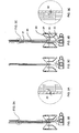
- the electrolytic plating apparatus includes a vibrator 11 attached to upper rod 13.
- the upper rod 13 is mounted with a spring system 12 to the rigid rod 14 that is used to support the v-saddles of the production line.
- the spring system 12 prevents vibration energy from being absorbed by the rigid parts of the apparatus.
- the upper rod 13 carries the vibration energy from vibrator 11 and produces homogeneous vibration energy to carry to lower rod 15.
- Clamps 16, in which the printed circuit boards are fixed, are connected to lower rod 15, as is flexible current-supply connection 17.
- the system includes a special floating shield 20 in which the venturi flow effect is increased. Electrolyte is supplied through piping 21 to eductors 22 so as to draw additional electrolyte from the bath.
- partitions 23 of floating shield 20 are shaped to enhance the venturi effect 25 of the eductors 22.
- Partition 24 is located directly below the printed circuit boards and acts to direct the flow to either side of the boards, depending on the location of the shield 20.
- the partitions 23 also assist in producing the improved laminar flow 26 along the printed circuit boards 31.
- the laminar flow 26 causes the formation of a low pressure region (i.e., Bernoulli effect) to draw an increased flow 33 of electrolyte through the through holes of the printed circuit boards 31, as illustrated in figure 2A .
- a low pressure region i.e., Bernoulli effect
- the laminar flow is directed to and increased on the opposite side of the printed circuit board by partitions 23 and 24 so as to cause the flow 32 of electrolyte in the opposite direction through the through hole.
- Figures 3A-E show the transition of the laminar flow and through hole flow from the having the transport mechanism move the shield and its partitions from the left ( figs. 3A-B ) of the eductors 22, to the middle ( fig. 3C ), and then to the right ( figs. 3D-E ) of the eductors 22.
- the present invention includes any electrolytic plating system with an elecrolytic plating bath, means for positioning the printed circuit boards in the bath, and means to alternately generate a laminar flow of electrolyte on each side of the printed circuit boards.
- a preferred means to alternately generate a laminar flow of electolyte comprises a floating shield with a venturi-shaped partition and an aligned partition below the printed circuit boards, and plurality of eductors below the floating shield.
- the means to alternately generate a laminar flow of electolyte can further comprise a transport mechanism that moves the floating shield and its partitions from side to side relative to the eductors or a mechanism to move the eductors.
- the plating can be further improved by using a vibrator and a spring-mounting system that prevents vibration energy being absorbed by fixed portions of the plating system.
- An exemplary embodiment of the invention is an electrolytic plating system for plating vias and thru-holes in printed circuit boards that includes an electrolyte bath, a lower rod above the bath, a flexible electrical current supply connection attached to the lower rod, at least one printed circuit board clamp attached to the lower rod, a floating shield with v-saddles in contact with the printed circuit boards, the floating shield further comprising a venturi-shaped partition, at least one eductor in a lower portion of the bath below the floating shield for producing a laminar flow of electrolyte across the printed circuit boards, and means to alternate the laminar flow from one side of the printed circuit board to an other side of the printed circuit board.
- This system could also further comprise an upper rod that supports the lower rod, a vibrator on the upper rod, and a spring system to mount the upper rod to a rigid structure.
- the floating shield could further comprise a partition directly below the printed circuit boards to direct flow of electrolyte to either side of the printed circuit boards and the means to alternate the laminar flow can be provided by a transport mechanism that moves the shield and its partitions from side to side relative to the eductors.
- the invention can also be limited to the improvement in vibration energy, such as an electrolytic plating system for printed circuit boards comprising a plating line supporting the printed circuit boards with a lower support rod, an upper rod that supports the lower rod, a vibrator on the upper rod, and a spring system to mount the upper rod to a rigid structure.
- vibration energy such as an electrolytic plating system for printed circuit boards comprising a plating line supporting the printed circuit boards with a lower support rod, an upper rod that supports the lower rod, a vibrator on the upper rod, and a spring system to mount the upper rod to a rigid structure.
- the method of practicing the present invention is an electrolytic plating method for plating vias and thru-holes in printed circuit boards that comprises positioning the printed circuit boards in an electrolytic bath and alternately generating a laminar flow of electrolyte on each side of the printed circuit boards.
- Alternately generating a laminar flow of electolyte can be provided by positioning a floating shield with a venturi-shaped partition and an aligned partition below the printed circuit boards; and operating a plurality of eductors below the floating shield, and can further comprise moving a transport mechanism so as to move the floating shield and its partitions from side to side relative to the eductors.
- the method can further include supplying vibration energy to the printed circuit boards in the bath by mounting a vibrator on the transport mechanism using a spring-mounting system to prevent vibration energy being absorbed by fixed supports.
- the electrolytic plating method for plating vias and thru-holes in printed circuit boards includes providing an electrolyte bath, positioning a lower rod above the bath, providing electrical current to the lower rod with a flexible connection, clamping at least one printed circuit board to the lower rod, transporting the printed circuit boards in a floating shield with v-saddles in contact with the printed circuit boards, the floating shield further positioning a venturi-shaped partition below the printed circuit boards, producing a laminar flow of electrolyte across the printed circuit boards with at least one eductor positioned in a lower portion of the bath below the floating shield, and alternating the laminar flow from one side of the printed circuit board to an other side of the printed circuit board.
- This method can further comprise supporting the lower rod with an upper rod, supplying vibration energy to the upper rod; and isolating the vibration energy from a fixed structure with a spring system, as well as providing a partition directly below the printed circuit boards to direct flow of electrolyte to either side of the printed circuit boards.
- moving a transport mechanism that moves the shield and its partitions from side to side relative to the eductors can be used to alternate the laminar flow.
- the electrolytic plating method for printed circuit boards of the present invention comprises supporting the printed circuit boards with a lower support rod of a plating line, supporting the lower rod with an upper rod, supplying vibration energy to the upper rod, and mounting the upper rod to a rigid structure with a spring system.
Landscapes
- Chemical & Material Sciences (AREA)
- Engineering & Computer Science (AREA)
- Chemical Kinetics & Catalysis (AREA)
- Electrochemistry (AREA)
- Materials Engineering (AREA)
- Metallurgy (AREA)
- Organic Chemistry (AREA)
- Physics & Mathematics (AREA)
- Electromagnetism (AREA)
- Optics & Photonics (AREA)
- Life Sciences & Earth Sciences (AREA)
- Sustainable Development (AREA)
- Manufacturing & Machinery (AREA)
- Microelectronics & Electronic Packaging (AREA)
- Electroplating Methods And Accessories (AREA)
- Manufacturing Of Printed Wiring (AREA)
- Printing Elements For Providing Electric Connections Between Printed Circuits (AREA)
Applications Claiming Priority (3)
| Application Number | Priority Date | Filing Date | Title |
|---|---|---|---|
| US34441701P | 2001-10-19 | 2001-10-19 | |
| US344417P | 2001-10-19 | ||
| PCT/US2002/033530 WO2003033770A2 (en) | 2001-10-19 | 2002-10-21 | System and method for electrolytic plating |
Publications (3)
| Publication Number | Publication Date |
|---|---|
| EP1438446A2 EP1438446A2 (en) | 2004-07-21 |
| EP1438446A4 EP1438446A4 (en) | 2006-03-29 |
| EP1438446B1 true EP1438446B1 (en) | 2012-06-20 |
Family
ID=23350458
Family Applications (1)
| Application Number | Title | Priority Date | Filing Date |
|---|---|---|---|
| EP02786452A Expired - Lifetime EP1438446B1 (en) | 2001-10-19 | 2002-10-21 | System and method for electrolytic plating |
Country Status (8)
| Country | Link |
|---|---|
| US (1) | US6818115B2 (OSRAM) |
| EP (1) | EP1438446B1 (OSRAM) |
| JP (1) | JP2005506447A (OSRAM) |
| KR (1) | KR100660086B1 (OSRAM) |
| CN (3) | CN101570873B (OSRAM) |
| AU (1) | AU2002349972B2 (OSRAM) |
| ES (1) | ES2449076T3 (OSRAM) |
| WO (1) | WO2003033770A2 (OSRAM) |
Families Citing this family (16)
| Publication number | Priority date | Publication date | Assignee | Title |
|---|---|---|---|---|
| JP4759834B2 (ja) * | 2001-04-25 | 2011-08-31 | 凸版印刷株式会社 | フィルムキャリア用電気めっき装置 |
| US20050061660A1 (en) * | 2002-10-18 | 2005-03-24 | Kempen Hein Van | System and method for electrolytic plating |
| EP1903129A1 (en) * | 2003-11-20 | 2008-03-26 | Process Automation International Limited | A liquid delivery system for an electroplating apparatus, an electroplating apparatus with such a liquid delivery system, and a method of operating an electroplating apparatus |
| US7947161B2 (en) * | 2004-03-19 | 2011-05-24 | Faraday Technology, Inc. | Method of operating an electroplating cell with hydrodynamics facilitating more uniform deposition on a workpiece with through holes |
| US7553401B2 (en) * | 2004-03-19 | 2009-06-30 | Faraday Technology, Inc. | Electroplating cell with hydrodynamics facilitating more uniform deposition across a workpiece during plating |
| JP2011256444A (ja) * | 2010-06-10 | 2011-12-22 | Sumitomo Bakelite Co Ltd | 基板の処理方法および処理装置 |
| NL2005480C2 (nl) * | 2010-10-07 | 2012-04-11 | Meco Equip Eng | Inrichting voor het eenzijdig elektrolytisch behandelen van een vlak substraat. |
| CN103590079A (zh) * | 2012-08-14 | 2014-02-19 | 亚洲电镀器材有限公司 | 一种电镀方法 |
| CN103320844A (zh) * | 2013-05-16 | 2013-09-25 | 陈焕宗 | 一种电镀工艺的面铜控制装置 |
| KR101457060B1 (ko) * | 2014-04-30 | 2014-10-31 | (주)네오피엠씨 | 진동전달기능을 갖는 도금장치 |
| CN105862098B (zh) * | 2016-06-22 | 2018-01-12 | 苏州翔邦达机电有限公司 | 适用于pcb板电镀的浮架系统 |
| JP2020147831A (ja) * | 2019-03-15 | 2020-09-17 | 三菱マテリアル株式会社 | 電解めっき装置、及び、電解めっき方法 |
| WO2021071885A1 (en) * | 2019-10-08 | 2021-04-15 | Applied Materials, Inc. | Mechanically-driven oscillating flow agitation |
| CN112822873A (zh) * | 2019-11-15 | 2021-05-18 | 宇泰和股份有限公司 | 高纵深比电路板通孔化学处理/电化学处理装置 |
| CN112111779A (zh) * | 2020-09-04 | 2020-12-22 | 深圳市欣佳宏科技有限公司 | 线路板电镀电源无线感应飞巴机构及电源无线感应方法 |
| KR102751572B1 (ko) * | 2024-05-23 | 2025-01-09 | (주)티피에스일렉콤 | 피도금물의 도금 품질 개선 및 광택 저하 방지를 위한 도금장치 |
Family Cites Families (9)
| Publication number | Priority date | Publication date | Assignee | Title |
|---|---|---|---|---|
| DE3015282C2 (de) * | 1980-04-21 | 1986-07-17 | Siemens AG, 1000 Berlin und 8000 München | Vorrichtung zum partiellen Galvanisieren von leitenden oder leitend gemachten Oberflächen |
| US4634503A (en) * | 1984-06-27 | 1987-01-06 | Daniel Nogavich | Immersion electroplating system |
| US4696729A (en) * | 1986-02-28 | 1987-09-29 | International Business Machines | Electroplating cell |
| JPH04500838A (ja) * | 1988-10-25 | 1992-02-13 | ベロルススキ ポリテフニチェスキ インスティテュト | 電気化学加工のための装置 |
| US4879007B1 (en) * | 1988-12-12 | 1999-05-25 | Process Automation Int L Ltd | Shield for plating bath |
| DE4106733A1 (de) * | 1991-03-02 | 1992-09-03 | Schering Ag | Vorrichtung zum abblenden von feldlinien in einer galvanikanlage (iii) |
| DE4337724A1 (de) * | 1993-11-05 | 1995-05-11 | Hoellmueller Maschbau H | Vorrichtung zur Beschichtung der Wandung von Bohrungen in elektrischen Leiterplatten oder Multilayern |
| JP2002121699A (ja) * | 2000-05-25 | 2002-04-26 | Nippon Techno Kk | めっき浴の振動流動とパルス状めっき電流との組み合わせを用いた電気めっき方法 |
| US20030010625A1 (en) * | 2001-07-16 | 2003-01-16 | Gramarossa Daniel J. | Processing cells for wafers and other planar articles |
-
2002
- 2002-10-18 US US10/273,820 patent/US6818115B2/en not_active Expired - Lifetime
- 2002-10-21 WO PCT/US2002/033530 patent/WO2003033770A2/en not_active Ceased
- 2002-10-21 CN CN2009101458143A patent/CN101570873B/zh not_active Expired - Fee Related
- 2002-10-21 KR KR1020047005787A patent/KR100660086B1/ko not_active Expired - Fee Related
- 2002-10-21 CN CNA2006101467242A patent/CN1962956A/zh active Pending
- 2002-10-21 AU AU2002349972A patent/AU2002349972B2/en not_active Ceased
- 2002-10-21 EP EP02786452A patent/EP1438446B1/en not_active Expired - Lifetime
- 2002-10-21 ES ES02786452.9T patent/ES2449076T3/es not_active Expired - Lifetime
- 2002-10-21 CN CNB028203887A patent/CN100523305C/zh not_active Expired - Fee Related
- 2002-10-21 JP JP2003536487A patent/JP2005506447A/ja active Pending
Also Published As
| Publication number | Publication date |
|---|---|
| KR20040058210A (ko) | 2004-07-03 |
| WO2003033770A2 (en) | 2003-04-24 |
| JP2005506447A (ja) | 2005-03-03 |
| HK1136011A1 (zh) | 2010-06-18 |
| US6818115B2 (en) | 2004-11-16 |
| CN101570873B (zh) | 2011-08-03 |
| US20030196904A1 (en) | 2003-10-23 |
| WO2003033770A3 (en) | 2003-09-18 |
| CN1962956A (zh) | 2007-05-16 |
| CN100523305C (zh) | 2009-08-05 |
| EP1438446A2 (en) | 2004-07-21 |
| ES2449076T3 (es) | 2014-03-18 |
| CN101570873A (zh) | 2009-11-04 |
| CN1571865A (zh) | 2005-01-26 |
| EP1438446A4 (en) | 2006-03-29 |
| AU2002349972B2 (en) | 2006-08-24 |
| KR100660086B1 (ko) | 2006-12-20 |
Similar Documents
| Publication | Publication Date | Title |
|---|---|---|
| EP1438446B1 (en) | System and method for electrolytic plating | |
| US8329006B2 (en) | Electroplating cell with hydrodynamics facilitating more uniform deposition across a workpiece during plating | |
| US7947161B2 (en) | Method of operating an electroplating cell with hydrodynamics facilitating more uniform deposition on a workpiece with through holes | |
| US20100176004A1 (en) | Apparatus and method for the electrolytic treatment of a plate-shaped product | |
| US6398937B1 (en) | Ultrasonically assisted plating bath for vias metallization in printed circuit board manufacturing | |
| AU2002349972A1 (en) | System and method for electrolytic plating | |
| US20250263862A1 (en) | Tsv process window and fill performance enhancement by long pulsing and ramping | |
| WO2019078063A1 (ja) | 表面処理装置 | |
| US20250361642A1 (en) | Plating device for improving plating quality and preventing gloss deterioration of objects to be plated | |
| CA2079033A1 (en) | Electroplating means for perforated printed circuit boards to be treated in a horizontal pass | |
| JP2004339590A (ja) | 表面処理装置 | |
| JPH0354887A (ja) | プリント基板の微小孔処理方法及びその装置 | |
| US12351935B2 (en) | Distribution system for a process fluid for chemical and/or electrolytic surface treatment of a substrate | |
| US20050061660A1 (en) | System and method for electrolytic plating | |
| HK40073051A (en) | Distribution system for a process fluid for chemical and/or electrolytic surface treatment of a substrate | |
| JPH0959797A (ja) | 自動液体処理ライン | |
| HK1136011B (en) | System and method for electrolytic plating | |
| Garich et al. | Effects of Plating Cell Configuration on the Quality of Copper Deposits for Printed Circuit Boards | |
| JPH0748587B2 (ja) | プリント配線板の電気メッキ方法及びその装置 | |
| JPH04354895A (ja) | 配線基板用電気めっき装置 | |
| JPH0361394A (ja) | 電解めっき装置 |
Legal Events
| Date | Code | Title | Description |
|---|---|---|---|
| PUAI | Public reference made under article 153(3) epc to a published international application that has entered the european phase |
Free format text: ORIGINAL CODE: 0009012 |
|
| 17P | Request for examination filed |
Effective date: 20040514 |
|
| AK | Designated contracting states |
Kind code of ref document: A2 Designated state(s): AT BE BG CH CY CZ DE DK EE ES FI FR GB GR IE IT LI LU MC NL PT SE SK TR |
|
| AX | Request for extension of the european patent |
Extension state: AL LT LV MK RO SI |
|
| RIC1 | Information provided on ipc code assigned before grant |
Ipc: 7C 25B 9/00 A |
|
| A4 | Supplementary search report drawn up and despatched |
Effective date: 20060209 |
|
| 17Q | First examination report despatched |
Effective date: 20061030 |
|
| REG | Reference to a national code |
Ref country code: DE Ref legal event code: R079 Ref document number: 60243195 Country of ref document: DE Free format text: PREVIOUS MAIN CLASS: C25B0009000000 Ipc: C25D0005020000 Ref country code: DE Ref legal event code: R079 Ref document number: 60243195 Country of ref document: DE Free format text: PREVIOUS MAIN CLASS: C25D0001000000 Ipc: C25D0005020000 |
|
| RIC1 | Information provided on ipc code assigned before grant |
Ipc: H05K 3/00 20060101ALI20111025BHEP Ipc: C25D 17/00 20060101ALI20111025BHEP Ipc: C25D 5/08 20060101ALI20111025BHEP Ipc: C25D 5/02 20060101AFI20111025BHEP |
|
| GRAP | Despatch of communication of intention to grant a patent |
Free format text: ORIGINAL CODE: EPIDOSNIGR1 |
|
| RAP1 | Party data changed (applicant data changed or rights of an application transferred) |
Owner name: VIASYSTEMS GROUP, INC. |
|
| RAP1 | Party data changed (applicant data changed or rights of an application transferred) |
Owner name: VIASYSTEMS GROUP, INC. |
|
| GRAS | Grant fee paid |
Free format text: ORIGINAL CODE: EPIDOSNIGR3 |
|
| GRAA | (expected) grant |
Free format text: ORIGINAL CODE: 0009210 |
|
| AK | Designated contracting states |
Kind code of ref document: B1 Designated state(s): AT BE BG CH CY CZ DE DK EE ES FI FR GB GR IE IT LI LU MC NL PT SE SK TR |
|
| REG | Reference to a national code |
Ref country code: GB Ref legal event code: FG4D |
|
| REG | Reference to a national code |
Ref country code: CH Ref legal event code: EP |
|
| REG | Reference to a national code |
Ref country code: AT Ref legal event code: REF Ref document number: 563133 Country of ref document: AT Kind code of ref document: T Effective date: 20120715 |
|
| REG | Reference to a national code |
Ref country code: IE Ref legal event code: FG4D |
|
| REG | Reference to a national code |
Ref country code: DE Ref legal event code: R096 Ref document number: 60243195 Country of ref document: DE Effective date: 20120816 |
|
| REG | Reference to a national code |
Ref country code: SE Ref legal event code: TRGR |
|
| REG | Reference to a national code |
Ref country code: NL Ref legal event code: T3 |
|
| PG25 | Lapsed in a contracting state [announced via postgrant information from national office to epo] |
Ref country code: GR Free format text: LAPSE BECAUSE OF FAILURE TO SUBMIT A TRANSLATION OF THE DESCRIPTION OR TO PAY THE FEE WITHIN THE PRESCRIBED TIME-LIMIT Effective date: 20120921 |
|
| PG25 | Lapsed in a contracting state [announced via postgrant information from national office to epo] |
Ref country code: EE Free format text: LAPSE BECAUSE OF FAILURE TO SUBMIT A TRANSLATION OF THE DESCRIPTION OR TO PAY THE FEE WITHIN THE PRESCRIBED TIME-LIMIT Effective date: 20120620 Ref country code: BE Free format text: LAPSE BECAUSE OF FAILURE TO SUBMIT A TRANSLATION OF THE DESCRIPTION OR TO PAY THE FEE WITHIN THE PRESCRIBED TIME-LIMIT Effective date: 20120620 Ref country code: CY Free format text: LAPSE BECAUSE OF FAILURE TO SUBMIT A TRANSLATION OF THE DESCRIPTION OR TO PAY THE FEE WITHIN THE PRESCRIBED TIME-LIMIT Effective date: 20120620 Ref country code: SK Free format text: LAPSE BECAUSE OF FAILURE TO SUBMIT A TRANSLATION OF THE DESCRIPTION OR TO PAY THE FEE WITHIN THE PRESCRIBED TIME-LIMIT Effective date: 20120620 |
|
| PG25 | Lapsed in a contracting state [announced via postgrant information from national office to epo] |
Ref country code: PT Free format text: LAPSE BECAUSE OF FAILURE TO SUBMIT A TRANSLATION OF THE DESCRIPTION OR TO PAY THE FEE WITHIN THE PRESCRIBED TIME-LIMIT Effective date: 20121022 |
|
| PGFP | Annual fee paid to national office [announced via postgrant information from national office to epo] |
Ref country code: AT Payment date: 20120927 Year of fee payment: 11 |
|
| PLBE | No opposition filed within time limit |
Free format text: ORIGINAL CODE: 0009261 |
|
| STAA | Information on the status of an ep patent application or granted ep patent |
Free format text: STATUS: NO OPPOSITION FILED WITHIN TIME LIMIT |
|
| PG25 | Lapsed in a contracting state [announced via postgrant information from national office to epo] |
Ref country code: CZ Free format text: LAPSE BECAUSE OF FAILURE TO SUBMIT A TRANSLATION OF THE DESCRIPTION OR TO PAY THE FEE WITHIN THE PRESCRIBED TIME-LIMIT Effective date: 20120620 Ref country code: DK Free format text: LAPSE BECAUSE OF FAILURE TO SUBMIT A TRANSLATION OF THE DESCRIPTION OR TO PAY THE FEE WITHIN THE PRESCRIBED TIME-LIMIT Effective date: 20120620 |
|
| REG | Reference to a national code |
Ref country code: NL Ref legal event code: V1 Effective date: 20130501 |
|
| 26N | No opposition filed |
Effective date: 20130321 |
|
| PG25 | Lapsed in a contracting state [announced via postgrant information from national office to epo] |
Ref country code: MC Free format text: LAPSE BECAUSE OF NON-PAYMENT OF DUE FEES Effective date: 20121031 |
|
| REG | Reference to a national code |
Ref country code: CH Ref legal event code: PL |
|
| GBPC | Gb: european patent ceased through non-payment of renewal fee |
Effective date: 20121021 |
|
| REG | Reference to a national code |
Ref country code: DE Ref legal event code: R097 Ref document number: 60243195 Country of ref document: DE Effective date: 20130321 |
|
| REG | Reference to a national code |
Ref country code: IE Ref legal event code: MM4A |
|
| REG | Reference to a national code |
Ref country code: FR Ref legal event code: ST Effective date: 20130628 |
|
| PG25 | Lapsed in a contracting state [announced via postgrant information from national office to epo] |
Ref country code: GB Free format text: LAPSE BECAUSE OF NON-PAYMENT OF DUE FEES Effective date: 20121021 Ref country code: DE Free format text: LAPSE BECAUSE OF NON-PAYMENT OF DUE FEES Effective date: 20130501 Ref country code: CH Free format text: LAPSE BECAUSE OF NON-PAYMENT OF DUE FEES Effective date: 20121031 Ref country code: SE Free format text: LAPSE BECAUSE OF NON-PAYMENT OF DUE FEES Effective date: 20121022 Ref country code: LI Free format text: LAPSE BECAUSE OF NON-PAYMENT OF DUE FEES Effective date: 20121031 Ref country code: IE Free format text: LAPSE BECAUSE OF NON-PAYMENT OF DUE FEES Effective date: 20121021 Ref country code: BG Free format text: LAPSE BECAUSE OF FAILURE TO SUBMIT A TRANSLATION OF THE DESCRIPTION OR TO PAY THE FEE WITHIN THE PRESCRIBED TIME-LIMIT Effective date: 20120920 |
|
| REG | Reference to a national code |
Ref country code: DE Ref legal event code: R119 Ref document number: 60243195 Country of ref document: DE Effective date: 20130501 |
|
| PG25 | Lapsed in a contracting state [announced via postgrant information from national office to epo] |
Ref country code: FI Free format text: LAPSE BECAUSE OF NON-PAYMENT OF DUE FEES Effective date: 20121021 Ref country code: IT Free format text: LAPSE BECAUSE OF NON-PAYMENT OF DUE FEES Effective date: 20121021 Ref country code: NL Free format text: LAPSE BECAUSE OF NON-PAYMENT OF DUE FEES Effective date: 20130501 Ref country code: FR Free format text: LAPSE BECAUSE OF NON-PAYMENT OF DUE FEES Effective date: 20121031 |
|
| REG | Reference to a national code |
Ref country code: ES Ref legal event code: FG2A Ref document number: 2449076 Country of ref document: ES Kind code of ref document: T3 Effective date: 20140318 |
|
| REG | Reference to a national code |
Ref country code: ES Ref legal event code: FD2A Effective date: 20140319 |
|
| PG25 | Lapsed in a contracting state [announced via postgrant information from national office to epo] |
Ref country code: TR Free format text: LAPSE BECAUSE OF FAILURE TO SUBMIT A TRANSLATION OF THE DESCRIPTION OR TO PAY THE FEE WITHIN THE PRESCRIBED TIME-LIMIT Effective date: 20120620 |
|
| PG25 | Lapsed in a contracting state [announced via postgrant information from national office to epo] |
Ref country code: ES Free format text: LAPSE BECAUSE OF NON-PAYMENT OF DUE FEES Effective date: 20121022 Ref country code: LU Free format text: LAPSE BECAUSE OF NON-PAYMENT OF DUE FEES Effective date: 20121021 |
|
| REG | Reference to a national code |
Ref country code: AT Ref legal event code: MM01 Ref document number: 563133 Country of ref document: AT Kind code of ref document: T Effective date: 20131021 |
|
| PG25 | Lapsed in a contracting state [announced via postgrant information from national office to epo] |
Ref country code: AT Free format text: LAPSE BECAUSE OF NON-PAYMENT OF DUE FEES Effective date: 20131021 |