EP1434359A1 - Verfahren zur Erzeugung einer mit einem externen Signal synchronisierten Folge sowie Synchronisationsschaltung und Empfänger - Google Patents
Verfahren zur Erzeugung einer mit einem externen Signal synchronisierten Folge sowie Synchronisationsschaltung und Empfänger Download PDFInfo
- Publication number
- EP1434359A1 EP1434359A1 EP02406139A EP02406139A EP1434359A1 EP 1434359 A1 EP1434359 A1 EP 1434359A1 EP 02406139 A EP02406139 A EP 02406139A EP 02406139 A EP02406139 A EP 02406139A EP 1434359 A1 EP1434359 A1 EP 1434359A1
- Authority
- EP
- European Patent Office
- Prior art keywords
- sequence
- feedback
- value
- values
- binary
- Prior art date
- Legal status (The legal status is an assumption and is not a legal conclusion. Google has not performed a legal analysis and makes no representation as to the accuracy of the status listed.)
- Granted
Links
- 238000000034 method Methods 0.000 title claims abstract description 35
- 230000001360 synchronised effect Effects 0.000 title claims abstract description 8
- 230000006870 function Effects 0.000 claims description 25
- PCHJSUWPFVWCPO-UHFFFAOYSA-N gold Chemical group [Au] PCHJSUWPFVWCPO-UHFFFAOYSA-N 0.000 claims description 13
- 230000008859 change Effects 0.000 claims description 3
- 238000002156 mixing Methods 0.000 claims description 2
- 238000011144 upstream manufacturing Methods 0.000 claims 2
- 230000000875 corresponding effect Effects 0.000 description 17
- 239000000872 buffer Substances 0.000 description 8
- 230000005540 biological transmission Effects 0.000 description 5
- 230000002349 favourable effect Effects 0.000 description 4
- 238000005265 energy consumption Methods 0.000 description 3
- 230000006399 behavior Effects 0.000 description 2
- 230000003111 delayed effect Effects 0.000 description 2
- 239000000203 mixture Substances 0.000 description 2
- 230000010363 phase shift Effects 0.000 description 2
- 230000008569 process Effects 0.000 description 2
- OKTJSMMVPCPJKN-UHFFFAOYSA-N Carbon Chemical compound [C] OKTJSMMVPCPJKN-UHFFFAOYSA-N 0.000 description 1
- 230000008901 benefit Effects 0.000 description 1
- 230000001413 cellular effect Effects 0.000 description 1
- 230000002596 correlated effect Effects 0.000 description 1
- 238000001914 filtration Methods 0.000 description 1
- 239000010931 gold Substances 0.000 description 1
- 229910052737 gold Inorganic materials 0.000 description 1
- 238000003384 imaging method Methods 0.000 description 1
- 230000006872 improvement Effects 0.000 description 1
- 230000010354 integration Effects 0.000 description 1
- 230000000737 periodic effect Effects 0.000 description 1
- 238000005070 sampling Methods 0.000 description 1
- 230000007480 spreading Effects 0.000 description 1
- 230000009466 transformation Effects 0.000 description 1
- 230000007704 transition Effects 0.000 description 1
- 230000003313 weakening effect Effects 0.000 description 1
Images





Classifications
-
- H—ELECTRICITY
- H04—ELECTRIC COMMUNICATION TECHNIQUE
- H04B—TRANSMISSION
- H04B1/00—Details of transmission systems, not covered by a single one of groups H04B3/00 - H04B13/00; Details of transmission systems not characterised by the medium used for transmission
- H04B1/69—Spread spectrum techniques
- H04B1/707—Spread spectrum techniques using direct sequence modulation
- H04B1/7073—Synchronisation aspects
- H04B1/7075—Synchronisation aspects with code phase acquisition
-
- G—PHYSICS
- G01—MEASURING; TESTING
- G01S—RADIO DIRECTION-FINDING; RADIO NAVIGATION; DETERMINING DISTANCE OR VELOCITY BY USE OF RADIO WAVES; LOCATING OR PRESENCE-DETECTING BY USE OF THE REFLECTION OR RERADIATION OF RADIO WAVES; ANALOGOUS ARRANGEMENTS USING OTHER WAVES
- G01S19/00—Satellite radio beacon positioning systems; Determining position, velocity or attitude using signals transmitted by such systems
- G01S19/01—Satellite radio beacon positioning systems transmitting time-stamped messages, e.g. GPS [Global Positioning System], GLONASS [Global Orbiting Navigation Satellite System] or GALILEO
- G01S19/13—Receivers
- G01S19/24—Acquisition or tracking or demodulation of signals transmitted by the system
- G01S19/30—Acquisition or tracking or demodulation of signals transmitted by the system code related
-
- H—ELECTRICITY
- H04—ELECTRIC COMMUNICATION TECHNIQUE
- H04J—MULTIPLEX COMMUNICATION
- H04J13/00—Code division multiplex systems
- H04J13/10—Code generation
Definitions
- the invention relates to a method for generating a internal sequence of analog values with a certain Period encoding one in a received signal corresponds to the external sequence and is synchronized with it, according to the preamble of claim 1, also a Synchronization circuit for performing the method and at least one such synchronization circuit comprehensive recipient.
- a Synchronization circuit for performing the method and at least one such synchronization circuit comprehensive recipient.
- the following as an example several of satellites must be used emitted signals assigned to the satellites and their Phase positions can be determined precisely, so that the running times and thus the distance of the receiver from the satellites can be determined.
- the transmission time of the The basic sequence is 1 ms, so the transmission time is one Chip of 1,023. Part of a millisecond, a little less than 1 ⁇ s.
- the satellite also transmits digital data by one Data bits with 20 in direct succession sent copies of the basic sequence is linked. Since the The transmission of the basic sequence takes 1 ms, the Data transmission at a rate of 50 bit / s.
- the received Signal therefore consists of a sequence of Repetitions of 20 times the basic sequence, being 20 times Depending on the data bit, the basic sequence is inverted or Not.
- the basic sequence is a so-called gold sequence.
- the signal is usually very weak and open a very negative signal-to-noise ratio on the decibel scale.
- the invention is based on the object to specify the generic method that with relatively little circuitry and low energy consumption a quick and reliable Identification of the basic sequence and determination of the External signal phase allowed. This task is characterized by the features in the characterizing part of the Claim 1 solved.
- Olsen Nonlinear binary sequences with asymptotically optimum periodic cross-correlation (dissertation University of California 1977). Also the ones described below Devices are, at most with insignificant Adjustments, in a far beyond the GPS system beyond the range of use.
- m-sequences gold sequences, Kasami sequences, etc., reference is made to the literature, for example EH Dinan, B. Jabbari: Spreading Codes for Direct Sequence CDMA and Wideband CDMA Cellular Networks, IEEE Communications Magazine 9/1998, Pp. 48-54.
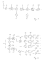
- the designed according to the invention shown in Fig. 1-4 GPS receiver has a high-frequency part (Fig. 1) with an antenna 1 for receiving the GPS satellites emitted signals on which a low noise self-regulating amplifier 2 and a bandpass filter 3 consequences.
- a first mixer stage with a Mixer 4, the amplified and filtered received Signal with a generated by an oscillator 5 Mixes a sinusoidal signal of 1,391.82 MHz and a bandpass filter 6 and a basically the same second Mixer stage with a mixer 7, the signal with a sine signal of frequency generated by an oscillator 8 180.6 MHz mixes and a bandpass filter 9.
- mixer stages are followed by an A / D converter 10.
- the signal path branches into an I and a Q path with one more each Mixing stage.
- the I path there is a mixer 11 in which the Signal with a generated by an oscillator 12 Sinusoidal signal of approximately 3 MHz is mixed while in the second there is another mixer 13, which is otherwise the same, in which the same signal with that through a Phase shifter 14 by 90 ° phase-shifted sinusoidal signal Oscillator 12 is mixed.
- the mixer 11 follows Low pass filter 15, behind which the path is in turn branches, namely to scanning elements 16, 17, to the first directly and secondly via a delay element 18, the the signal is delayed by a ⁇ T of approx. 0.5 ⁇ s.
- To the mixer 13 connects a circuit of exactly the same structure.
- the baseband section has a total of eight outputs, from which everyone with the receipt of a number of their own Synchronization circuits are connected, each one is assigned to certain satellites and to those of it used basic sequence synchronized.
- the buffer 19 comprises (FIG. 3) an adder 21 and a shift register 22 with 1,023 storage locations for analog values.
- the output of the shift register 22 is fed back to the second input of the adder 21.
- Each synchronization circuit (FIG. 4) comprises a logic element 23 following the input, which is followed by an adder 24 and further an analog feedback shift register 25 with ten memory locations.
- a feedback circuit 26 is connected to taps at the tenth memory location and one or more additional memory locations. In the example, (5), there is only one additional tap at the third memory location.
- the tapped analog values are linked in the feedback circuit 26 in accordance with a feedback function.
- the graph of a possible feedback function with two arguments f (x 1 , x 2 ) is shown in FIG. 5.
- the output of the feedback circuit 26 is connected to the second input of the adder 24 via a scaler 27.
- the adder 24 thus forms a superimposition circuit for superimposing a feedback value with an intermediate value coming from the logic element 23
- the output of the scaler 27 is also a Discriminator 28 connected to a square or a others the input signal in the positive range imaging circuit, a low pass filter and one Contains threshold detector and emits a binary signal.
- the discriminator can also be anywhere else that of the shift register 25, the feedback circuit 26, the scaler 27 and the adder 24 formed loop be connected.
- a shift register 29 provided that one of all in the shift register 25th stored determination derived binary Values are fed and its output with the second Input of the logic circuit 23 is connected.
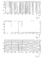
- FIG. 6 shows a section of the basic sequence of the GPS satellite with the number 1 that lasts 100 ⁇ s.
- This basic sequence is a gold sequence, which consists of a first generating m-sequence p 1 , ..., p 1 '023 , which is defined by the feedback according to (5), and a second generating m-sequence q 1 , .. ., q 1 '023 can be generated.
- FIG. 7 shows the first 10 ⁇ s of the detail from FIG. 6.
- the basic sequence is coded in the satellite in a carrier signal with a frequency of 1,575.42 MHz, in such a way that each change in the binary value in the same by a phase jump by 180 ° is represented in the carrier signal.
- the signal thus prepared that shown in FIG Section corresponds to that shown in FIG. 8.
- the signal is in the A / D converter 10 with a certain bit width, e.g. 12 bits for the amount and an additional bit for the Sign digitized.
- the values can be as Floating point numbers or as whole numbers. However, they will be used to distinguish from binary Values referred to as analog values. In the figures are noisy signals are shown, while actually the very weak signals are very noisy in the antenna with a typical signal-to-noise ratio of approx. -35dB.
- mixers 11 and 12 are now mixed with Sinusoidal signals of approximately 3 MHz that in FIGS. 9 and 10 shown signals generated.
- the frequency of the oscillator 12 is controllable. Because depending the current state of motion of a satellite Carrier frequency must be Doppler shifted by a few kHz a corresponding frequency range, e.g. be swept gradually. For this purpose, then the frequency of the oscillator 12 can be varied in a targeted manner.
- the signal is now in the I- as well as in the Q-path via one Low pass filter 15, the high-frequency components filtered out, fed directly to the sensing element 16 and over the delay element 18 the sensing element 17.
- a ⁇ T of approx. 0.5 ⁇ s which is a corresponds to half the chip length in the delay element 18 ensures that at least one scan at well-defined signal.
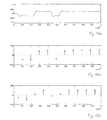
- 11a is the signal of the 1-path after the low-pass filter 15, i.e. before the 11b shows the sequence of the analog Values that the scanning element 16 generates therefrom and in FIG. 11c the analog values at the output of the scanning element 17.
- Figures 12a-c are the corresponding signals of the Q path shown.
- the corresponding analog values are now stored in the buffer 19.
- the basic sequence stored in the buffer 19 now becomes Generation of an external sequence read out repeatedly and each to the inputs of two synchronization circuits (Fig. 4) directed to the one directly and to the other, since the basic sequence is linked to the Data bit can be inverted, via an inverter 20.
- the external sequence corresponds to repetitions of the basic sequence which contains the noisy basic sequence s 1 , ..., s 1 '023 , the same according to (6) by linking the first generating m-sequence p 1 , ..., p 1' 023 and the second generating m-sequence q 1 , ..., q 1'023 is generated.
- the shift register 25 generates the first generating m-sequence in the synchronized state.
- the content of the shift register 25, a i-10, ..., ai-1 thus corresponds to a section of this m-sequence, ie P i-10, ..., P i-1 for any i with 1 ⁇ i ⁇ 1,023.
- this i can be clearly determined and thus the corresponding value q i of the second generating sequence.
- This value is read from the memory 29, which is structured as a table with 1,023 storage locations, the sign bits of the values p i-10, ... p i-1 being used as a determination record, which is then used as the address of the Table space of q i serves.
- the next link of the external sequence which, apart from a noise component, essentially corresponds to s i , is linked in the link 23 with q i , which according to (6) in conjunction with (1) essentially results in p i as an intermediate value.
- This value is added in the adder 24 to the feedback value from the feedback circuit 26 scaled in the scaler 27.
- this latter value is also substantially p i, since he through which the first generating sequence defining feedback from the substantially P i-10, ..., p i-1, corresponding values of a i-10, ... , a i-1 , in the specific case by linking a i-10 with a i-3 .
- the superimposition of the feedback value with the intermediate value thus corresponds to a i and is fed into the shift register 25 as a new input value.
- the system is obviously consistent.
- the sequence of a i generated in the analog feedback shift register 25 essentially corresponds to repetitions of the first generating m sequence p 1 ,..., P 1 '023 .
- By linking them with the second generating m-sequence q 1 , ..., q 1 '023 a repetition of the basic sequence s 1 , ..., s 1' 023 can be generated.
- the amount of the feedback value should be slightly less than 1, preferably between 0.90 and 0.99. It is favorable if the feedback function supplies a value of 1 for arguments of the amount 1, ie (7)
- 1 for
- 1, applies and the function value is then multiplied by a selectable factor k ⁇ 1, in particular 0.90 ⁇ k ⁇ 0.99. This multiplication is carried out by the adjustable scaler 27, which is connected downstream of the feedback circuit 26 evaluating the feedback function.
- the feedback function f is invariant by swapping the arguments. As a function of each individual argument, i.e. if the the rest, it should be antisymmetric and monotone.
- This function is a linear combination of the arguments with coefficients of +1 or -1 in each sector, except for a scaling that ensures that (7) is fulfilled.
- the criterion for successful synchronization is the power of the generated internal sequence, which is taken off at the output of the scaler 27. While the elements of the internal sequence have approximately the same value as those of the external sequence before a synchronization, the latter is amplified by a factor 1 / (1-k), that is usually between 10 and 100, when synchronization has taken place.
- the performance of the internal sequence (a i ) i 1 , ..., 1'023 accordingly rises sharply, as shown in FIG. 13.
- the discriminator 28 in which the power is determined by squaring and filtering is smoothed by a low-pass filter and averaged over a longer period of time and finally the result is compared with a threshold value. It emits a corresponding binary signal that indicates the synchronization that has taken place.
- the lack of synchronization can be random, e.g. a particularly unfavorable form of Are due to an unfavorable phase position of the received signal or an unfavorable Sampling time before a data bit change, which leads to that in the buffers 19 (FIG. 2), copies of sequences are added in which the one containing the basic sequence sought Proportion with different signs occurs, which leads to a serious weakening of the said portion can lead to the noise component. In such cases it is useful to fill the buffers 19 with new basic sequences and to restart the synchronization process with them.
- the GPS system uses up to 32 satellites each, the basic sequences of which differ. Since the signals from all satellites in the reception area should be used, the receiver should contain all types of synchronization circuits corresponding to all satellites in use, each type synchronizing with the basic sequence of one of the satellites. The types differ either in the content of the memory, which determines the second generating m-sequence q 1 , ..., q 1 '023 .
- the branching to the different types can instead of at the end of the baseband part, where 32 different synchronization circuits can be connected to each output, also lie further ahead in the signal path, for example at the end of the high-frequency part. This has the advantage that the frequency of the oscillator 12 can be adjusted more specifically to the orbit of the respective satellite using further information. On the other hand, a multiplication of the entire baseband part is of course necessary.
- the described embodiment can of course many species are modified. For example, other than the intermediate frequencies mentioned are selected or the Intermediate stages are completely or partially eliminated.
- the shift registers can e.g. each from a corresponding memory with linear addressing and a write and a read pointer are formed.
Landscapes
- Engineering & Computer Science (AREA)
- Computer Networks & Wireless Communication (AREA)
- Radar, Positioning & Navigation (AREA)
- Remote Sensing (AREA)
- Signal Processing (AREA)
- Physics & Mathematics (AREA)
- General Physics & Mathematics (AREA)
- Position Fixing By Use Of Radio Waves (AREA)
- Mobile Radio Communication Systems (AREA)
- Synchronisation In Digital Transmission Systems (AREA)
Abstract
Description
- Fig. 1
- im wesentlichen ein Hochfrequenzteil eines erfindungsgemässen Empfängers,
- Fig. 2
- ein Basisbandteil des besagten Empfängers,
- Fig. 3
- eine Komponente des Basisbandteils,
- Fig. 4
- eine erfindungsgemässe Synchronisationsschaltung,
- Fig. 5
- den Graphen einer im erfindungsgemässen Verfahren verwendeten Rückkopplungsfunktion,
- Fig. 6
- einen Ausschnitt aus einer Gold-Folge, wie sie im Signal eines GPS-Satelliten codiert ist,
- Fig. 7
- vergrössert einen Ausschnitt aus der Gold-Folge von Fig. 6,
- Fig. 8
- einen dem Ausschnitt von Fig. 6 entsprechenden Ausschnitt des Signals am Ende des Hochfrequenzteils,
- Fig.9, 10
- dem Ausschnitt von Fig. 6 entsprechende Ausschnitte des Signals an bestimmten Punkten des Basisbandteils,
- Fig. 11a-c, 12a-c
- dem Ausschnitt von Fig. 6 entsprechende Ausschnitte des Signals an weiteren Punkten des Basisbandteils und
- Fig. 13
- die Entwicklung der Leistung eines Rückkopplungssignals im Basisbandteil während einer Synchronisation.
| b2\b1 | 0 | 1 |
| 0 | 0 | 1 |
| 1 | 1 | 0 |
| P2\P1 | -1 | 1 |
| - 1 | -1 | 1 |
| 1 | 1 | -1 |
- 1
- Antenne
- 2
- Verstärker
- 3
- Bandpassfilter
- 4
- Mischer
- 5
- Oszillator
- 6
- Bandpassfilter
- 7
- Mischer
- 8
- Oszillator
- 9
- Bandpassfilter
- 10
- A/D-Wandler
- 11
- Mischer
- 12
- Oszillator
- 13
- Mischer
- 14
- Phasenschieber
- 15
- Tiefpassfilter
- 16
- Abtastglied
- 17
- Abtastglied
- 18
- Verzögerungsglied
- 19
- Puffer
- 20
- Invertierer
- 21
- Addierer
- 22
- Schieberegister
- 23
- Verknüpfungsglied
- 24
- Addierer
- 25
- Schieberegister
- 26
- Rückkopplungsschaltung
- 27
- Skalierer
- 28
- Diskriminator
- 29
- Speicher
Claims (23)
- Verfahren zur Erzeugung einer internen Folge von analogen Werten mit einer bestimmten Periode, welche einer in einem empfangenen Signal codierten externen Folge entspricht und mit ihr synchron ist, wobei die externe Folge Wiederholungen einer Grundfolge (s1,...,sN) der Länge N umfasst, welche im wesentlichen einer Folge von binären Werten entspricht, die durch Verknüpfung einer ersten erzeugenden Binärfolge (p1,...,pN) der Länge N mit einer nicht konstanten zweiten erzeugenden Binärfolge (q1,...,qN) der Länge N herstellbar ist und wobei die erste erzeugende Binärfolge (p1,...,pN) durch ein binäres rückgekoppeltes Schieberegister der Länge n, in welchem ein nächster Wert (pi) jeweils durch binäre Verknüpfung des ältesten Wertes (pi-n) mit mindestens einem der auf diesen folgenden Werte (Pi-n+1,....,Pi-1) gemäss einem festen Rückkopplungsmuster hergestellt wird, erzeugbar ist und in der kein Abschnitt der Länge n öfter als ein Mal auftritt, so dass gegebenenfalls die Position eines derartigen Abschnitts innerhalb der Grundfolge (s1,...,sN) eindeutig bestimmt ist, dadurch gekennzeichnet, dass dem Eingang eines analogen rückgekoppelten Schieberegisters der Länge n mit einem demjenigen des besagten binären rückgekoppelten Schieberegisters entsprechenden Rückkopplungsmuster jeweils ein neuer Eingangswert (ai) zugeführt wird, welcher durch Ueberlagerung eines aus den Werten (ai-n,...,ai-1) im analogen rückgekoppelten Schieberegister gemäss einer Rückkopplungsfunktion abgeleiteten analogen Rückkopplungswerts mit einem Zwischenwert hergestellt wird, der gegebenenfalls durch Verknüpfung des aktuellen Wertes der externen Folge mit einem aktuellen Wert (qi) der zweiten erzeugenden Folge (q1,...,qN) hergestellt wurde, dessen Position (i) in derselben auf die Position eines Abschnitts in der ersten erzeugenden Folge (p1,...,pN) folgt, welcher aus einem Bestimmungssatz von n binären Werten besteht, die aus den analogen Werten (ai-n,...,ai-1) im analogen rückgekoppelten Schieberegister abgeleitet wurden.
- Verfahren nach Anspruch 1, dadurch gekennzeichnet, dass die erste erzeugende Folge (p1,...,pN) eine m-Folge der Länge N=2n-1 ist, derart, dass jeder Satz von n binären Werten ausser einem genau ein Mal als Abschnitt der Länge n in derselben vorkommt.
- Verfahren nach Anspruch 2, dadurch gekennzeichnet, dass es sich bei der Grundfolge um eine Gold-Folge handelt.
- Verfahren nach einem der Ansprüche 1 bis 3, dadurch gekennzeichnet, dass der aktuelle Wert (qi) der zweiten erzeugenden Binärfolge (q1,...,qN) jeweils mit dem Bestimmungssatz als Adresse aus einer Tabelle ausgelesen wird.
- Verfahren nach einem der Ansprüche 1 bis 4, dadurch gekennzeichnet, dass die binären Folgen jeweils aus den Werten +1 und -1 bestehen und die Verknüpfung bis auf einen allfälligen Vorzeichenwechsel die Multiplikation ist.
- Verfahren nach Anspruch 5, dadurch gekennzeichnet, dass der Betrag der Rückkopplungsfunktion 1 ist, wenn die Beträge der Argumente jeweils 1 sind.
- Verfahren nach Anspruch 5 oder 6, dadurch gekennzeichnet, dass das Vorzeichen der Rückkopplungsfunktion stets dem Vorzeichen der Verknüpfung der Argumente entspricht.
- Verfahren nach einem der Ansprüche 5 bis 7, dadurch gekennzeichnet, dass die Rückkopplungsfunktion invariant unter Vertauschung der Argumente ist.
- Verfahren nach einem der Ansprüche 5 bis 8, dadurch gekennzeichnet, dass die Rückkopplungsfunktion als Funktion eines jeden Argumentes antisymmetrisch und monoton ist.
- Verfahren nach einem der Ansprüche 5 bis 9, dadurch gekennzeichnet, dass die Rückkopplungsfunktion im wesentlichen innerhalb eines jeden durch bestimmte Werte der Vorzeichen der Argumente gekennzeichneten Sektors im wesentlichen eine Linearkombination der Argumente ist.
- Verfahren nach Anspruch 10, dadurch gekennzeichnet, dass der Betrag der Rückkopplungsfunktion im wesentlichen dem Mittelwert der Beträge der Argumente entspricht.
- Verfahren nach einem der Ansprüche 6 bis 11, dadurch gekennzeichnet, dass der Rückkopplungswert durch Multiplikation des Wertes der Rückkopplungsfunktion mit einem Faktor k<1, der vorzugsweise zwischen 0,90 und 0,99 liegt, hergestellt wird.
- Verfahren nach einem der Ansprüche 5 bis 12, dadurch gekennzeichnet, dass der Bestimmungssatz aus den binären Werten besteht, welche jeweils das gleiche Vorzeichen haben wie der entsprechende analoge Wert (ai-n;...;ai-1) im Schieberegister.
- Verfahren nach einem der Ansprüche 1 bis 13, dadurch gekennzeichnet, dass die externe Folge mehrere zeitlich unmittelbar aufeinanderfolgende Kopien einer aus dem empfangenen Signal abgeleiteten Basisfolge umfasst, deren Länge der Länge N der Grundfolge entspricht.
- Verfahren nach Anspruch 14, dadurch gekennzeichnet, dass die Basisfolge erzeugt wird, indem die Werte mehrerer in zeitlicher Aufeinanderfolge vom empfangenen Signal abgeleiteter Folgen der Länge N aufaddiert werden.
- Verfahren nach einem der Ansprüche 1 bis 15, dadurch gekennzeichnet, dass ein erfolgte Synchronisation anzeigendes binäres Ausgangssignal erzeugt wird, wenn die Beträge der Werte (ai) der internen Folge einen Schwellwert überschreiten.
- Synchronisationsschaltung zur Durchführung des Verfahrens nach einem der Ansprüche 1 bis 16, mit einem Eingang zur Aufnahme einer von einem empfangenen Signal abgeleiteten externen Folge von analogen Werten und einem analogen rückgekoppelten Schieberegister (25), einer nach einem bestimmten Rückkopplungsmuster mit Abgriffen desselben verbundenen Rückkopplungsschaltung (26) zur Auswertung einer Rückkopplungsfunktion für die Bestimmung eines Rückkopplungswertes und einer Ueberlagerungsschaltung zur Ueberlagerung des Rückkopplungswertes mit einem Zwischenwert, dadurch gekennzeichnet, dass sie ausserdem einen Speicher (29) umfasst, aus dem jeweils gemäss einer Tabelle mit einer von den im analogen rückgekoppelten Schieberegister (25) gespeicherten Werten abgeleiteten Bestimmungssatz als Adresse ein Wert auslesbar ist, sowie ein Verknüpfungsglied (23) zur Herstellung des Zwischenwerts durch Verknüpfung des ausgelesenen Wertes mit dem am Eingang anliegenden Wert.
- Synchronisationsschaltung nach Anspruch 17, dadurch gekennzeichnet, dass der Rückkopplungsschaltung (26) ein Skalierer (27) zur Herstellung des Rückkopplungswertes aus ihrem Ausgangswert nachgeschaltet ist und die Ueberlagerungsschaltung als Addierer (24) zur Addition des Rückkopplungswertes zum Zwischenwert ausgebildet ist.
- Synchronisationsschaltung nach Anspruch 17 oder 18, dadurch gekennzeichnet, dass sie einen Diskriminator (28) zur Erzeugung eines erfolgte Synchronisation anzeigenden binären Ausgangssignals umfasst, dessen Eingang mit dem Ausgang der Rückkopplungsschaltung (26) verbunden ist und der vorzugsweise einen Quadrierer, einen Tiefpassfilter und einen Schwellwertdetektor umfasst.
- Empfänger zum Empfang eines Signals, welcher mindestens eine Synchronisationsschaltung nach einem der Ansprüche 17 bis 19 zur Ableitung einer internen Folge aus dem empfangenen Signal umfasst.
- Empfänger nach Anspruch 20, dadurch gekennzeichnet, dass er mindestens ein Paar von gleichen Synchronisationsschaltungen umfasst, von denen die eine über einen Invertierer (20) und die andere direkt mit einem gemeinsamen Eingang verbunden sind.
- Empfänger nach Anspruch 20 oder 21, dadurch gekennzeichnet, dass er mindestens ein Paar von gleichen Synchronisationsschaltungen umfasst, welche jeweils über ein Abtastglied (16; 17) mit einem gemeinsamen Eingang verbunden sind, wobei mindestens einem Abtastglied (17) ein Verzögerungsglied (18) vorgeschaltet ist, welches die abgetasteten Werte jeweils um einen Teil einer Chiplänge verschiebt.
- Empfänger nach einem der Ansprüche 20 bis 22, dadurch gekennzeichnet, dass er einen Oszillator (12) zur Erzeugung eines ersten sinusförmigen Signals und eines gegenüber demselben um 90° phasenverschobenen zweiten sinusförmigen Signals umfasst sowie mindestens ein Paar von gleichen Synchronisationsschaltungen, jeweils mit einem vorgeschalteten Mischer (11; 13) zur Mischung des empfangenen Signals mit dem ersten sinusförmiges Signal bzw. dem zweiten sinusförmigen Signal.
Priority Applications (5)
| Application Number | Priority Date | Filing Date | Title |
|---|---|---|---|
| ES02406139T ES2245725T3 (es) | 2002-12-24 | 2002-12-24 | Procedimiento para generar una sucesion sincronizable con una señal externa, asi como circuito de sincronizacion y receptor. |
| DE50203698T DE50203698D1 (de) | 2002-12-24 | 2002-12-24 | Verfahren zur Erzeugung einer mit einem externen Signal synchronisierten Folge sowie Synchronisationsschaltung und Empfänger |
| AT02406139T ATE300125T1 (de) | 2002-12-24 | 2002-12-24 | Verfahren zur erzeugung einer mit einem externen signal synchronisierten folge sowie synchronisationsschaltung und empfänger |
| EP02406139A EP1434359B1 (de) | 2002-12-24 | 2002-12-24 | Verfahren zur Erzeugung einer mit einem externen Signal synchronisierten Folge sowie Synchronisationsschaltung und Empfänger |
| US10/617,657 US7212565B2 (en) | 2002-12-24 | 2003-07-14 | Method for producing a sequence synchronized with an external signal and synchronization circuit and receiver |
Applications Claiming Priority (1)
| Application Number | Priority Date | Filing Date | Title |
|---|---|---|---|
| EP02406139A EP1434359B1 (de) | 2002-12-24 | 2002-12-24 | Verfahren zur Erzeugung einer mit einem externen Signal synchronisierten Folge sowie Synchronisationsschaltung und Empfänger |
Publications (2)
| Publication Number | Publication Date |
|---|---|
| EP1434359A1 true EP1434359A1 (de) | 2004-06-30 |
| EP1434359B1 EP1434359B1 (de) | 2005-07-20 |
Family
ID=32405828
Family Applications (1)
| Application Number | Title | Priority Date | Filing Date |
|---|---|---|---|
| EP02406139A Expired - Lifetime EP1434359B1 (de) | 2002-12-24 | 2002-12-24 | Verfahren zur Erzeugung einer mit einem externen Signal synchronisierten Folge sowie Synchronisationsschaltung und Empfänger |
Country Status (5)
| Country | Link |
|---|---|
| US (1) | US7212565B2 (de) |
| EP (1) | EP1434359B1 (de) |
| AT (1) | ATE300125T1 (de) |
| DE (1) | DE50203698D1 (de) |
| ES (1) | ES2245725T3 (de) |
Families Citing this family (1)
| Publication number | Priority date | Publication date | Assignee | Title |
|---|---|---|---|---|
| JP4282520B2 (ja) * | 2004-03-24 | 2009-06-24 | シャープ株式会社 | 信号処理方法、信号出力装置、信号処理装置、画像処理装置、及び画像形成装置 |
Citations (2)
| Publication number | Priority date | Publication date | Assignee | Title |
|---|---|---|---|---|
| US5737360A (en) * | 1995-06-19 | 1998-04-07 | International Business Machines, Corp. | System employing continuous-time dissipative pseudorandom dynamics for communications and measurement |
| WO2001037441A2 (en) * | 1999-11-15 | 2001-05-25 | Massachusetts Institute Of Technology | A nonlinear dynamic system for spread spectrum code generation and acquisition |
Family Cites Families (2)
| Publication number | Priority date | Publication date | Assignee | Title |
|---|---|---|---|---|
| US4114155A (en) * | 1976-07-30 | 1978-09-12 | Cincinnati Electronics Corporation | Position determining apparatus and method |
| US7529291B2 (en) * | 2004-04-13 | 2009-05-05 | Raytheon Company | Methods and structures for rapid code acquisition in spread spectrum communications |
-
2002
- 2002-12-24 DE DE50203698T patent/DE50203698D1/de not_active Expired - Lifetime
- 2002-12-24 EP EP02406139A patent/EP1434359B1/de not_active Expired - Lifetime
- 2002-12-24 ES ES02406139T patent/ES2245725T3/es not_active Expired - Lifetime
- 2002-12-24 AT AT02406139T patent/ATE300125T1/de active
-
2003
- 2003-07-14 US US10/617,657 patent/US7212565B2/en not_active Expired - Lifetime
Patent Citations (2)
| Publication number | Priority date | Publication date | Assignee | Title |
|---|---|---|---|---|
| US5737360A (en) * | 1995-06-19 | 1998-04-07 | International Business Machines, Corp. | System employing continuous-time dissipative pseudorandom dynamics for communications and measurement |
| WO2001037441A2 (en) * | 1999-11-15 | 2001-05-25 | Massachusetts Institute Of Technology | A nonlinear dynamic system for spread spectrum code generation and acquisition |
Non-Patent Citations (1)
| Title |
|---|
| VIGODA BENJAMIN: "A Nonlinear Dynamic System for Spread Spectrum Code Acquisition", MASTERS THESIS; MIT MEDIA LAB, 9 August 1999 (1999-08-09), Boston, US, pages 1 - 90, XP002167577, Retrieved from the Internet <URL:www.media.mit.edu/physics/publications/theses/99.06.vigoda.pdf> [retrieved on 20010516] * |
Also Published As
| Publication number | Publication date |
|---|---|
| EP1434359B1 (de) | 2005-07-20 |
| ES2245725T3 (es) | 2006-01-16 |
| DE50203698D1 (de) | 2005-08-25 |
| ATE300125T1 (de) | 2005-08-15 |
| US20040120439A1 (en) | 2004-06-24 |
| US7212565B2 (en) | 2007-05-01 |
Similar Documents
| Publication | Publication Date | Title |
|---|---|---|
| DE69734693T2 (de) | Sequenzerzeugung für asynchrone Spreizspektrumübertragung | |
| EP1825631B1 (de) | Synchronisationsvorrichtung und vorrichtung zum erzeugen eines synchronisationssignals | |
| DE69628885T2 (de) | Empfänger und verfahren zur erzeugung von spreizcodes in einem empfänger | |
| DE69635370T2 (de) | Cdma datenübertragungsverfahren, sender und empfänger mit benutzung eines supersymbols zur interferenzeliminierung | |
| DE2800898A1 (de) | Mit gedehntem frequenzspektrum arbeitendes nachrichtenuebertragungssystem | |
| WO2008000428A1 (de) | Empfänger und verfahren zum empfangen eines ersten nutzfrequenzbandes und eines zweiten nutzfrequenzbandes | |
| DE3047942A1 (de) | Verfahren zum schalten eines empfaengers und korrelators | |
| DE60303185T2 (de) | Verfahren, System und elektronisches Gerät zur Synchronisation eines Empfängers | |
| DE69924277T2 (de) | Verfahren und schaltung für die erzeugung einer variablen taktfrequenz | |
| DE102007003796B4 (de) | Verfahren und Vorrichtung für das Bestimmen von Grenzen von Informationselementen | |
| DE3546307A1 (de) | Digitale speichereinrichtung | |
| DE60021019T2 (de) | Spreizspektrumempfänger | |
| EP1434359B1 (de) | Verfahren zur Erzeugung einer mit einem externen Signal synchronisierten Folge sowie Synchronisationsschaltung und Empfänger | |
| DE19958613B4 (de) | Codephaseneinstellverfahren und -Codierer | |
| EP1252725B1 (de) | Einrichtung zur durchführung von suchprozeduren in einem mobilfunkempfänger | |
| DE10049525B4 (de) | Vorrichtung und Verfahren zur Berechnung eines Korrelationswertes entsprechend einem Frequenzfehler und Speichermedium mit einem gespeicherten Korrelationswert-Berechnungsprogramm | |
| DE60124817T2 (de) | Synchronisationdetektionsgerät | |
| WO2006063765A1 (de) | Vorrichtung und verfahren zum bestimmen eines korrelationswertes | |
| WO2006063768A1 (de) | Vorrichtung und verfahren zum bestimmen eines eintreffzeitpunktes einer empfangsfolge | |
| EP1434360B1 (de) | Synchronisationsschaltung | |
| DE19919545B4 (de) | Verfahren zur Bildung einer Signalfolge | |
| DE2824444A1 (de) | Schaltungsanordnung zum dekodieren | |
| DE60001481T2 (de) | Verfahren zur partiellen Korrelation in einem CDMA-Empfänger | |
| DE60206501T2 (de) | Mehrzweigigdiskriminatormodul für ein navigationssystem | |
| DE102005034009B4 (de) | Verfahren und Vorrichtung zum Verkürzen von pseudozufälligen Spreizsequenzen auf eine vorgegebene Länge für ein Codemultiplex-Zugriffsverfahren |
Legal Events
| Date | Code | Title | Description |
|---|---|---|---|
| PUAI | Public reference made under article 153(3) epc to a published international application that has entered the european phase |
Free format text: ORIGINAL CODE: 0009012 |
|
| 17P | Request for examination filed |
Effective date: 20040122 |
|
| AK | Designated contracting states |
Kind code of ref document: A1 Designated state(s): AT BE BG CH CY CZ DE DK EE ES FI FR GB GR IE IT LI LU MC NL PT SE SI SK TR |
|
| AX | Request for extension of the european patent |
Extension state: AL LT LV MK RO |
|
| GRAP | Despatch of communication of intention to grant a patent |
Free format text: ORIGINAL CODE: EPIDOSNIGR1 |
|
| AKX | Designation fees paid |
Designated state(s): AT BE BG CH CY CZ DE DK EE ES FI FR GB GR IE IT LI LU MC NL PT SE SI SK TR |
|
| GRAS | Grant fee paid |
Free format text: ORIGINAL CODE: EPIDOSNIGR3 |
|
| GRAA | (expected) grant |
Free format text: ORIGINAL CODE: 0009210 |
|
| AK | Designated contracting states |
Kind code of ref document: B1 Designated state(s): AT BE BG CH CY CZ DE DK EE ES FI FR GB GR IE IT LI LU MC NL PT SE SI SK TR |
|
| PG25 | Lapsed in a contracting state [announced via postgrant information from national office to epo] |
Ref country code: SI Free format text: LAPSE BECAUSE OF FAILURE TO SUBMIT A TRANSLATION OF THE DESCRIPTION OR TO PAY THE FEE WITHIN THE PRESCRIBED TIME-LIMIT Effective date: 20050720 Ref country code: NL Free format text: LAPSE BECAUSE OF FAILURE TO SUBMIT A TRANSLATION OF THE DESCRIPTION OR TO PAY THE FEE WITHIN THE PRESCRIBED TIME-LIMIT Effective date: 20050720 Ref country code: SK Free format text: LAPSE BECAUSE OF FAILURE TO SUBMIT A TRANSLATION OF THE DESCRIPTION OR TO PAY THE FEE WITHIN THE PRESCRIBED TIME-LIMIT Effective date: 20050720 Ref country code: CZ Free format text: LAPSE BECAUSE OF FAILURE TO SUBMIT A TRANSLATION OF THE DESCRIPTION OR TO PAY THE FEE WITHIN THE PRESCRIBED TIME-LIMIT Effective date: 20050720 Ref country code: EE Free format text: LAPSE BECAUSE OF FAILURE TO SUBMIT A TRANSLATION OF THE DESCRIPTION OR TO PAY THE FEE WITHIN THE PRESCRIBED TIME-LIMIT Effective date: 20050720 Ref country code: TR Free format text: LAPSE BECAUSE OF FAILURE TO SUBMIT A TRANSLATION OF THE DESCRIPTION OR TO PAY THE FEE WITHIN THE PRESCRIBED TIME-LIMIT Effective date: 20050720 |
|
| REG | Reference to a national code |
Ref country code: GB Ref legal event code: FG4D Free format text: NOT ENGLISH |
|
| REG | Reference to a national code |
Ref country code: CH Ref legal event code: EP |
|
| REG | Reference to a national code |
Ref country code: IE Ref legal event code: FG4D Free format text: LANGUAGE OF EP DOCUMENT: GERMAN |
|
| REF | Corresponds to: |
Ref document number: 50203698 Country of ref document: DE Date of ref document: 20050825 Kind code of ref document: P |
|
| REG | Reference to a national code |
Ref country code: CH Ref legal event code: NV Representative=s name: ZIMMERLI, WAGNER & PARTNER AG |
|
| PG25 | Lapsed in a contracting state [announced via postgrant information from national office to epo] |
Ref country code: GR Free format text: LAPSE BECAUSE OF FAILURE TO SUBMIT A TRANSLATION OF THE DESCRIPTION OR TO PAY THE FEE WITHIN THE PRESCRIBED TIME-LIMIT Effective date: 20051020 Ref country code: DK Free format text: LAPSE BECAUSE OF FAILURE TO SUBMIT A TRANSLATION OF THE DESCRIPTION OR TO PAY THE FEE WITHIN THE PRESCRIBED TIME-LIMIT Effective date: 20051020 Ref country code: BG Free format text: LAPSE BECAUSE OF FAILURE TO SUBMIT A TRANSLATION OF THE DESCRIPTION OR TO PAY THE FEE WITHIN THE PRESCRIBED TIME-LIMIT Effective date: 20051020 |
|
| GBT | Gb: translation of ep patent filed (gb section 77(6)(a)/1977) |
Effective date: 20051010 |
|
| REG | Reference to a national code |
Ref country code: SE Ref legal event code: TRGR |
|
| RAP2 | Party data changed (patent owner data changed or rights of a patent transferred) |
Owner name: U-BLOX AG |
|
| PG25 | Lapsed in a contracting state [announced via postgrant information from national office to epo] |
Ref country code: PT Free format text: LAPSE BECAUSE OF FAILURE TO SUBMIT A TRANSLATION OF THE DESCRIPTION OR TO PAY THE FEE WITHIN THE PRESCRIBED TIME-LIMIT Effective date: 20051221 |
|
| PG25 | Lapsed in a contracting state [announced via postgrant information from national office to epo] |
Ref country code: CY Free format text: LAPSE BECAUSE OF FAILURE TO SUBMIT A TRANSLATION OF THE DESCRIPTION OR TO PAY THE FEE WITHIN THE PRESCRIBED TIME-LIMIT Effective date: 20051224 |
|
| PG25 | Lapsed in a contracting state [announced via postgrant information from national office to epo] |
Ref country code: LU Free format text: LAPSE BECAUSE OF NON-PAYMENT OF DUE FEES Effective date: 20051231 Ref country code: MC Free format text: LAPSE BECAUSE OF NON-PAYMENT OF DUE FEES Effective date: 20051231 |
|
| NLT2 | Nl: modifications (of names), taken from the european patent patent bulletin |
Owner name: U-BLOX AG Effective date: 20051109 |
|
| REG | Reference to a national code |
Ref country code: ES Ref legal event code: FG2A Ref document number: 2245725 Country of ref document: ES Kind code of ref document: T3 |
|
| NLV1 | Nl: lapsed or annulled due to failure to fulfill the requirements of art. 29p and 29m of the patents act | ||
| ET | Fr: translation filed | ||
| PLBE | No opposition filed within time limit |
Free format text: ORIGINAL CODE: 0009261 |
|
| STAA | Information on the status of an ep patent application or granted ep patent |
Free format text: STATUS: NO OPPOSITION FILED WITHIN TIME LIMIT |
|
| 26N | No opposition filed |
Effective date: 20060421 |
|
| REG | Reference to a national code |
Ref country code: CH Ref legal event code: PFA Owner name: U-BLOX-AG Free format text: U-BLOX-AG#ZUERCHERSTRASSE 68#8800 THALWIL (CH) -TRANSFER TO- U-BLOX-AG#ZUERCHERSTRASSE 68#8800 THALWIL (CH) |
|
| REG | Reference to a national code |
Ref country code: CH Ref legal event code: NV Representative=s name: WAGNER PATENT AG, CH |
|
| PGFP | Annual fee paid to national office [announced via postgrant information from national office to epo] |
Ref country code: CH Payment date: 20141219 Year of fee payment: 13 Ref country code: ES Payment date: 20141226 Year of fee payment: 13 Ref country code: SE Payment date: 20141219 Year of fee payment: 13 Ref country code: IE Payment date: 20141222 Year of fee payment: 13 Ref country code: FI Payment date: 20141211 Year of fee payment: 13 |
|
| PGFP | Annual fee paid to national office [announced via postgrant information from national office to epo] |
Ref country code: AT Payment date: 20141222 Year of fee payment: 13 |
|
| PGFP | Annual fee paid to national office [announced via postgrant information from national office to epo] |
Ref country code: IT Payment date: 20141219 Year of fee payment: 13 |
|
| PGFP | Annual fee paid to national office [announced via postgrant information from national office to epo] |
Ref country code: BE Payment date: 20141219 Year of fee payment: 13 |
|
| REG | Reference to a national code |
Ref country code: FR Ref legal event code: PLFP Year of fee payment: 14 |
|
| PG25 | Lapsed in a contracting state [announced via postgrant information from national office to epo] |
Ref country code: BE Free format text: LAPSE BECAUSE OF NON-PAYMENT OF DUE FEES Effective date: 20151231 |
|
| REG | Reference to a national code |
Ref country code: CH Ref legal event code: PL |
|
| REG | Reference to a national code |
Ref country code: SE Ref legal event code: EUG |
|
| REG | Reference to a national code |
Ref country code: AT Ref legal event code: MM01 Ref document number: 300125 Country of ref document: AT Kind code of ref document: T Effective date: 20151224 |
|
| PG25 | Lapsed in a contracting state [announced via postgrant information from national office to epo] |
Ref country code: SE Free format text: LAPSE BECAUSE OF NON-PAYMENT OF DUE FEES Effective date: 20151225 |
|
| REG | Reference to a national code |
Ref country code: IE Ref legal event code: MM4A |
|
| PG25 | Lapsed in a contracting state [announced via postgrant information from national office to epo] |
Ref country code: CH Free format text: LAPSE BECAUSE OF NON-PAYMENT OF DUE FEES Effective date: 20151231 Ref country code: IE Free format text: LAPSE BECAUSE OF NON-PAYMENT OF DUE FEES Effective date: 20151224 Ref country code: LI Free format text: LAPSE BECAUSE OF NON-PAYMENT OF DUE FEES Effective date: 20151231 |
|
| PG25 | Lapsed in a contracting state [announced via postgrant information from national office to epo] |
Ref country code: AT Free format text: LAPSE BECAUSE OF NON-PAYMENT OF DUE FEES Effective date: 20151224 |
|
| REG | Reference to a national code |
Ref country code: FR Ref legal event code: PLFP Year of fee payment: 15 |
|
| PG25 | Lapsed in a contracting state [announced via postgrant information from national office to epo] |
Ref country code: IT Free format text: LAPSE BECAUSE OF NON-PAYMENT OF DUE FEES Effective date: 20151224 |
|
| REG | Reference to a national code |
Ref country code: ES Ref legal event code: FD2A Effective date: 20170203 |
|
| PG25 | Lapsed in a contracting state [announced via postgrant information from national office to epo] |
Ref country code: ES Free format text: LAPSE BECAUSE OF NON-PAYMENT OF DUE FEES Effective date: 20151225 |
|
| PG25 | Lapsed in a contracting state [announced via postgrant information from national office to epo] |
Ref country code: FI Free format text: LAPSE BECAUSE OF NON-PAYMENT OF DUE FEES Effective date: 20151224 |
|
| REG | Reference to a national code |
Ref country code: FR Ref legal event code: PLFP Year of fee payment: 16 |
|
| PGFP | Annual fee paid to national office [announced via postgrant information from national office to epo] |
Ref country code: DE Payment date: 20191210 Year of fee payment: 18 |
|
| PGFP | Annual fee paid to national office [announced via postgrant information from national office to epo] |
Ref country code: FR Payment date: 20191219 Year of fee payment: 18 |
|
| PGFP | Annual fee paid to national office [announced via postgrant information from national office to epo] |
Ref country code: GB Payment date: 20191220 Year of fee payment: 18 |
|
| REG | Reference to a national code |
Ref country code: DE Ref legal event code: R119 Ref document number: 50203698 Country of ref document: DE |
|
| GBPC | Gb: european patent ceased through non-payment of renewal fee |
Effective date: 20201224 |
|
| PG25 | Lapsed in a contracting state [announced via postgrant information from national office to epo] |
Ref country code: FR Free format text: LAPSE BECAUSE OF NON-PAYMENT OF DUE FEES Effective date: 20201231 |
|
| PG25 | Lapsed in a contracting state [announced via postgrant information from national office to epo] |
Ref country code: DE Free format text: LAPSE BECAUSE OF NON-PAYMENT OF DUE FEES Effective date: 20210701 Ref country code: GB Free format text: LAPSE BECAUSE OF NON-PAYMENT OF DUE FEES Effective date: 20201224 |