EP1432023A1 - Semiconductor device and production method therefor - Google Patents
Semiconductor device and production method therefor Download PDFInfo
- Publication number
- EP1432023A1 EP1432023A1 EP02770176A EP02770176A EP1432023A1 EP 1432023 A1 EP1432023 A1 EP 1432023A1 EP 02770176 A EP02770176 A EP 02770176A EP 02770176 A EP02770176 A EP 02770176A EP 1432023 A1 EP1432023 A1 EP 1432023A1
- Authority
- EP
- European Patent Office
- Prior art keywords
- semiconductor device
- hole
- groove
- layer
- manufacturing
- Prior art date
- Legal status (The legal status is an assumption and is not a legal conclusion. Google has not performed a legal analysis and makes no representation as to the accuracy of the status listed.)
- Ceased
Links
Images



Classifications
-
- H—ELECTRICITY
- H10—SEMICONDUCTOR DEVICES; ELECTRIC SOLID-STATE DEVICES NOT OTHERWISE PROVIDED FOR
- H10W—GENERIC PACKAGES, INTERCONNECTIONS, CONNECTORS OR OTHER CONSTRUCTIONAL DETAILS OF DEVICES COVERED BY CLASS H10
- H10W20/00—Interconnections in chips, wafers or substrates
- H10W20/01—Manufacture or treatment
- H10W20/071—Manufacture or treatment of dielectric parts thereof
- H10W20/074—Manufacture or treatment of dielectric parts thereof of dielectric parts comprising thin functional dielectric layers, e.g. dielectric etch-stop, barrier, capping or liner layers
- H10W20/077—Manufacture or treatment of dielectric parts thereof of dielectric parts comprising thin functional dielectric layers, e.g. dielectric etch-stop, barrier, capping or liner layers on sidewalls or on top surfaces of conductors
-
- H—ELECTRICITY
- H10—SEMICONDUCTOR DEVICES; ELECTRIC SOLID-STATE DEVICES NOT OTHERWISE PROVIDED FOR
- H10W—GENERIC PACKAGES, INTERCONNECTIONS, CONNECTORS OR OTHER CONSTRUCTIONAL DETAILS OF DEVICES COVERED BY CLASS H10
- H10W20/00—Interconnections in chips, wafers or substrates
- H10W20/01—Manufacture or treatment
-
- H—ELECTRICITY
- H10—SEMICONDUCTOR DEVICES; ELECTRIC SOLID-STATE DEVICES NOT OTHERWISE PROVIDED FOR
- H10P—GENERIC PROCESSES OR APPARATUS FOR THE MANUFACTURE OR TREATMENT OF DEVICES COVERED BY CLASS H10
- H10P14/00—Formation of materials, e.g. in the shape of layers or pillars
- H10P14/60—Formation of materials, e.g. in the shape of layers or pillars of insulating materials
- H10P14/65—Formation of materials, e.g. in the shape of layers or pillars of insulating materials characterised by treatments performed before or after the formation of the materials
- H10P14/6516—Formation of materials, e.g. in the shape of layers or pillars of insulating materials characterised by treatments performed before or after the formation of the materials of treatments performed after formation of the materials
- H10P14/6518—Formation of materials, e.g. in the shape of layers or pillars of insulating materials characterised by treatments performed before or after the formation of the materials of treatments performed after formation of the materials by introduction of substances into an already-existing insulating layer
- H10P14/6524—Formation of materials, e.g. in the shape of layers or pillars of insulating materials characterised by treatments performed before or after the formation of the materials of treatments performed after formation of the materials by introduction of substances into an already-existing insulating layer the substance being nitrogen
- H10P14/6526—Formation of materials, e.g. in the shape of layers or pillars of insulating materials characterised by treatments performed before or after the formation of the materials of treatments performed after formation of the materials by introduction of substances into an already-existing insulating layer the substance being nitrogen introduced into an oxide material, e.g. changing SiO to SiON
-
- H—ELECTRICITY
- H10—SEMICONDUCTOR DEVICES; ELECTRIC SOLID-STATE DEVICES NOT OTHERWISE PROVIDED FOR
- H10P—GENERIC PROCESSES OR APPARATUS FOR THE MANUFACTURE OR TREATMENT OF DEVICES COVERED BY CLASS H10
- H10P14/00—Formation of materials, e.g. in the shape of layers or pillars
- H10P14/60—Formation of materials, e.g. in the shape of layers or pillars of insulating materials
- H10P14/65—Formation of materials, e.g. in the shape of layers or pillars of insulating materials characterised by treatments performed before or after the formation of the materials
- H10P14/6516—Formation of materials, e.g. in the shape of layers or pillars of insulating materials characterised by treatments performed before or after the formation of the materials of treatments performed after formation of the materials
- H10P14/6529—Formation of materials, e.g. in the shape of layers or pillars of insulating materials characterised by treatments performed before or after the formation of the materials of treatments performed after formation of the materials by exposure to a gas or vapour
- H10P14/6532—Formation of materials, e.g. in the shape of layers or pillars of insulating materials characterised by treatments performed before or after the formation of the materials of treatments performed after formation of the materials by exposure to a gas or vapour by exposure to a plasma
-
- H—ELECTRICITY
- H10—SEMICONDUCTOR DEVICES; ELECTRIC SOLID-STATE DEVICES NOT OTHERWISE PROVIDED FOR
- H10P—GENERIC PROCESSES OR APPARATUS FOR THE MANUFACTURE OR TREATMENT OF DEVICES COVERED BY CLASS H10
- H10P95/00—Generic processes or apparatus for manufacture or treatments not covered by the other groups of this subclass
-
- H—ELECTRICITY
- H10—SEMICONDUCTOR DEVICES; ELECTRIC SOLID-STATE DEVICES NOT OTHERWISE PROVIDED FOR
- H10W—GENERIC PACKAGES, INTERCONNECTIONS, CONNECTORS OR OTHER CONSTRUCTIONAL DETAILS OF DEVICES COVERED BY CLASS H10
- H10W20/00—Interconnections in chips, wafers or substrates
- H10W20/01—Manufacture or treatment
- H10W20/071—Manufacture or treatment of dielectric parts thereof
-
- H—ELECTRICITY
- H10—SEMICONDUCTOR DEVICES; ELECTRIC SOLID-STATE DEVICES NOT OTHERWISE PROVIDED FOR
- H10W—GENERIC PACKAGES, INTERCONNECTIONS, CONNECTORS OR OTHER CONSTRUCTIONAL DETAILS OF DEVICES COVERED BY CLASS H10
- H10W20/00—Interconnections in chips, wafers or substrates
- H10W20/01—Manufacture or treatment
- H10W20/071—Manufacture or treatment of dielectric parts thereof
- H10W20/074—Manufacture or treatment of dielectric parts thereof of dielectric parts comprising thin functional dielectric layers, e.g. dielectric etch-stop, barrier, capping or liner layers
-
- H—ELECTRICITY
- H10—SEMICONDUCTOR DEVICES; ELECTRIC SOLID-STATE DEVICES NOT OTHERWISE PROVIDED FOR
- H10W—GENERIC PACKAGES, INTERCONNECTIONS, CONNECTORS OR OTHER CONSTRUCTIONAL DETAILS OF DEVICES COVERED BY CLASS H10
- H10W20/00—Interconnections in chips, wafers or substrates
- H10W20/01—Manufacture or treatment
- H10W20/071—Manufacture or treatment of dielectric parts thereof
- H10W20/074—Manufacture or treatment of dielectric parts thereof of dielectric parts comprising thin functional dielectric layers, e.g. dielectric etch-stop, barrier, capping or liner layers
- H10W20/076—Manufacture or treatment of dielectric parts thereof of dielectric parts comprising thin functional dielectric layers, e.g. dielectric etch-stop, barrier, capping or liner layers in via holes or trenches
-
- H—ELECTRICITY
- H10—SEMICONDUCTOR DEVICES; ELECTRIC SOLID-STATE DEVICES NOT OTHERWISE PROVIDED FOR
- H10W—GENERIC PACKAGES, INTERCONNECTIONS, CONNECTORS OR OTHER CONSTRUCTIONAL DETAILS OF DEVICES COVERED BY CLASS H10
- H10W20/00—Interconnections in chips, wafers or substrates
- H10W20/01—Manufacture or treatment
- H10W20/071—Manufacture or treatment of dielectric parts thereof
- H10W20/081—Manufacture or treatment of dielectric parts thereof by forming openings in the dielectric parts
- H10W20/084—Manufacture or treatment of dielectric parts thereof by forming openings in the dielectric parts for dual-damascene structures
-
- H—ELECTRICITY
- H10—SEMICONDUCTOR DEVICES; ELECTRIC SOLID-STATE DEVICES NOT OTHERWISE PROVIDED FOR
- H10W—GENERIC PACKAGES, INTERCONNECTIONS, CONNECTORS OR OTHER CONSTRUCTIONAL DETAILS OF DEVICES COVERED BY CLASS H10
- H10W20/00—Interconnections in chips, wafers or substrates
- H10W20/01—Manufacture or treatment
- H10W20/071—Manufacture or treatment of dielectric parts thereof
- H10W20/093—Manufacture or treatment of dielectric parts thereof by modifying materials of the dielectric parts
- H10W20/096—Manufacture or treatment of dielectric parts thereof by modifying materials of the dielectric parts by contacting with gases, liquids or plasmas
-
- H—ELECTRICITY
- H10—SEMICONDUCTOR DEVICES; ELECTRIC SOLID-STATE DEVICES NOT OTHERWISE PROVIDED FOR
- H10P—GENERIC PROCESSES OR APPARATUS FOR THE MANUFACTURE OR TREATMENT OF DEVICES COVERED BY CLASS H10
- H10P14/00—Formation of materials, e.g. in the shape of layers or pillars
- H10P14/60—Formation of materials, e.g. in the shape of layers or pillars of insulating materials
- H10P14/63—Formation of materials, e.g. in the shape of layers or pillars of insulating materials characterised by the formation processes
- H10P14/6302—Non-deposition formation processes
- H10P14/6319—Formation by plasma treatments, e.g. plasma oxidation of the substrate
-
- H—ELECTRICITY
- H10—SEMICONDUCTOR DEVICES; ELECTRIC SOLID-STATE DEVICES NOT OTHERWISE PROVIDED FOR
- H10P—GENERIC PROCESSES OR APPARATUS FOR THE MANUFACTURE OR TREATMENT OF DEVICES COVERED BY CLASS H10
- H10P14/00—Formation of materials, e.g. in the shape of layers or pillars
- H10P14/60—Formation of materials, e.g. in the shape of layers or pillars of insulating materials
- H10P14/63—Formation of materials, e.g. in the shape of layers or pillars of insulating materials characterised by the formation processes
- H10P14/6326—Deposition processes
- H10P14/6328—Deposition from the gas or vapour phase
- H10P14/6334—Deposition from the gas or vapour phase using decomposition or reaction of gaseous or vapour phase compounds, i.e. chemical vapour deposition
- H10P14/6336—Deposition from the gas or vapour phase using decomposition or reaction of gaseous or vapour phase compounds, i.e. chemical vapour deposition in the presence of a plasma [PECVD]
-
- H—ELECTRICITY
- H10—SEMICONDUCTOR DEVICES; ELECTRIC SOLID-STATE DEVICES NOT OTHERWISE PROVIDED FOR
- H10P—GENERIC PROCESSES OR APPARATUS FOR THE MANUFACTURE OR TREATMENT OF DEVICES COVERED BY CLASS H10
- H10P14/00—Formation of materials, e.g. in the shape of layers or pillars
- H10P14/60—Formation of materials, e.g. in the shape of layers or pillars of insulating materials
- H10P14/69—Inorganic materials
- H10P14/692—Inorganic materials composed of oxides, glassy oxides or oxide-based glasses
- H10P14/6921—Inorganic materials composed of oxides, glassy oxides or oxide-based glasses containing silicon
- H10P14/6922—Inorganic materials composed of oxides, glassy oxides or oxide-based glasses containing silicon the material containing Si, O and at least one of H, N, C, F or other non-metal elements, e.g. SiOC, SiOC:H or SiONC
- H10P14/6927—Inorganic materials composed of oxides, glassy oxides or oxide-based glasses containing silicon the material containing Si, O and at least one of H, N, C, F or other non-metal elements, e.g. SiOC, SiOC:H or SiONC the material being a silicon oxynitride, e.g. SiON or SiON:H
-
- H—ELECTRICITY
- H10—SEMICONDUCTOR DEVICES; ELECTRIC SOLID-STATE DEVICES NOT OTHERWISE PROVIDED FOR
- H10P—GENERIC PROCESSES OR APPARATUS FOR THE MANUFACTURE OR TREATMENT OF DEVICES COVERED BY CLASS H10
- H10P14/00—Formation of materials, e.g. in the shape of layers or pillars
- H10P14/60—Formation of materials, e.g. in the shape of layers or pillars of insulating materials
- H10P14/69—Inorganic materials
- H10P14/694—Inorganic materials composed of nitrides
- H10P14/6943—Inorganic materials composed of nitrides containing silicon
- H10P14/69433—Inorganic materials composed of nitrides containing silicon the material being a silicon nitride not containing oxygen, e.g. SixNy or SixByNz
Definitions
- the present invention relates to a semiconductor device with a high reliability, and a manufacturing method thereof.
- Speeding up of signal processing is necessary, for achieving high efficiency of large-scale integration circuits (LSIs).
- Speeding up of signal processing can be carried out by miniaturization of circuits and reducing signal delay on interconnection.
- miniaturizing has progressed, and designing rule of LSI has reached to 0.13 micrometers, and reduction in signal delay on interconnection is especially important in this kind of LSI.
- Reduction in a resistance of interconnections is the effective means for reducing the above signal delay on interconnections.
- copper which has a high electro-migration tolerance and has a low resistance, is used instead of aluminum which has been conventionally used. Because processing of the conventional etching is difficult in a case where copper interconnection (wiring) is used, the so called Dual Damascene method is used for realizing multi-layered interconnection, without etching the copper.
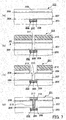
- a process of manufacturing a semiconductor device 201, which comprises a multi-layered interconnection layer, using the Dual Damascene method will be described with reference to FIGS. 7 (a) to (d).
- a cap layer 204 made of silicon nitride, etc. is formed on a first insulating layer 203 made of silicon oxide, etc., where an interconnection (wiring) layer 202 is embedded.
- the interconnection layer 202 surrounds a conductor layer 205 made of copper, and a conductor layer 205, and comprises a barrier layer 206 made of tantalum nitride, etc.
- a second insulating layer 207 made of silicon oxide, etc. is formed on the cap layer 204.
- result abstructures shown in FIG. 7 (a) can be obtained.
- a resist pattern 210 is formed on the third insulating layer 209, and a hole 211 having the conductor layer 205 as bottom, by etching, is formed. At this time, etching is carried out on the condition that the second and third insulating films 207 and 209, the stopper film 208, and the cap layer 204 are etched. After etching, the resist pattern 210 is removed by ashing, etc.
- a resists pattern 212 is formed on the third insulating film 209. And an interconnection groove 213 which overlaps with the hole 211 and has the stopper film 208 as the bottom, is formed on the third insulating film 209.
- the interconnection groove 213, and the interconnection hole 214 that connects the interconnection groove 213 and the interconnection layer 202 is formed.
- etching is carried out on the condition that the third insulating film 209 is etched, but the stopper film 208 is not. Therefore, etching is stopped at the stopper film 208. After etching, the resist pattern 212 is removed by ashing, etc.
- the barrier layer 215 is provided to prevent diffusion of copper, which is interconnection material. Because copper is highly diffusive, and is inclined to deteriorate the characteristic of the semiconductor, the barrier layer 215 is a necessity in forming interconnection layers made of copper. Especially, in recent years, because the porous films that are preferably used for the reason that the dielectric constant is low, has many holes in the interior, copper atoms are likely to penetrate (diffuse).
- the barrier layer 215 is generally structured singularly by metal material such as titanium nitride, and tantalum nitride, etc., or by being laminated, and is formed by CVD, etc.
- metal material such as titanium nitride, and tantalum nitride, etc.
- CVD etc.
- the interconnection hole 214 is extremely minute, infilteration of precursors (organic metal, etc.) of the barrier layer 215 is physically prevented, and deposition speed in the lower part becomes slower than the upper part of the interconnection hole 214.
- a barrier layer 215 with enough thickness is not formed in the lower part of the interconnection hole 214, and barrier characteristic deteriorates.
- the barrier layer 215 is uneven, void becomes likely to occur in the latter copper embedding process.
- the thickness of the barrier layer 215 becomes thinner, and the adhesiveness to the surface of the interconnection groove 213 and the interconnection hole 214 is deteriorated.
- peeling off, etc., of the barrier layer 215 becomes likely to occur, and reliability of the barrier layer 215 and the semiconductor device 201 degrades. In this way, it is difficult to form a highly reliable barrier layer at the inner wall of a highly miniaturized (with a high aspect ratio) groove or hole.
- the stopper film 208 of etching is used. As shown in FIG. 7 (d), the stopper film 208 forms the bottom part of the interconnection groove 213. Accompanying the progress of miniaturization, thinning of the stopper film 208 is also being sought. Therefore, in the same way as the above barrier layer 215, in a case where a thin film stopper film 208 formed by CVD, etc., is used, adhesiveness with the second insulating film 207 deteriorates, and peeling off becomes likely to occur. In the case where the stopper film 208 is peeled off, etc., the barrier layer 215 stacked thereon becomes uneven, and lowly reliable.
- an object of the present invention is to provide a highly reliable semiconductor device and manufacturing method thereof.
- Another object of the present invention is to provide a semiconductor device which comprises a highly reliable barrier layer, and manufacturing method thereof.
- Still another object of the present invention is to provide a semiconductor device which comprises a highly reliable stopper film, and manufacturing method thereof.
- a manufacturing method of a semiconductor device is characterized by comprising:
- a barrier layer made of silicon nitride film is formed at the inner wall of an interconnection groove and an interconnection hole, where interconnection material (especially copper) is embedded.
- Silicon nitride film that constitutes the barrier layer is formed by reforming the surface region of the insulating layers made of a film including silicon, by plasma of nitrogen gas. In this way, by directly reforming the surface of the insulating layers, a thin barrier layer can be formed with a high reliability at the inner wall of a groove and hole, which is minute and has a high aspect ratio. By this, a highly reliable semiconductor device where diffusion of interconnection material is reduced, can be provided.
- the barrier layer forming step comprises a step of nitriding the surface region of the groove and the hole by exposing the surface of the inner wall of the groove and the hole to the plasma of gas including nitrogen.
- the barrier layer by forming the barrier layer by direct nitriding of the insulating layers, a thin barrier layer with little peeling off, etc., can be formed.
- the plasma of gas including nitrogen is generated by irradiating microwave from a plane antenna that comprises a plurality of slits to gas including nitrogen.
- a thin barrier layer can be formed, reducing plasma damage provided to other film surfaces.
- the insulating layers may be structured by porous dielectric film.
- metal precursor such as organic metal, etc.
- the barrier layer metal precursor such as organic metal, etc.
- metal precursors, etc. do not enter the hole in the insulating layers.
- deterioration of insulating layers occurred by reaction, etc., of metal precursors and etching gas in the hole is prevented, and a highly reliable semiconductor device can be obtained.
- a manufacturing method of a semiconductor device is characterized by comprising:
- the stopper film made of silicon nitride film is formed by surface modification by plasma.
- the formed stopper film is a film with little plasma damage on the surface and of high quality.
- the stopper film that comprises the bottom part of the interconnection groove can be formed with at high reliability.
- the step of forming the stopper film comprises a step of nitriding the surface region of the first insulating layer by exposing the surface of the first insulating layer to the plasma of gas including nitrogen.
- the stopper film by forming the stopper film by direct nitriding of the insulating films, a thin stopper film with little peeling off, can be formed controlling surface damage.
- the first and second insulating layers may be structured by porous dielectric film.
- copper may be used as the main component, as the conductive material.
- the silicon nitride film has barrier characteristics towards copper, and functions effectively as the barrier layer.
- gas including hydrogen may be further used as the above gas.
- hydrogen can be combined with the dangling bond of silicon that exists at the surface region of the insulating layers, so that the film can be stabilized.
- the forming of the barrier layer is carried out at room temperature to 600°C.
- the barrier layer may be formed in a thickness of 1nm to 20nm.
- the stopper film may be formed in a thickness of 1nm to 20nm.
- a semiconductor device is characterized by comprising:
- a semiconductor device is characterized by comprising:
- a barrier layer made of silicon nitride film is formed at the inner wall of an interconnection groove and an interconnection hole, where interconnection material (especially copper) is embedded.
- a silicon nitride film that constitutes the barrier layer is formed in the surface region of the insulating layers made of a film including silicon by microwave plasma applying radial line slot antenna (RLSA).
- RLSA radial line slot antenna
- a semiconductor device is characterized by comprising:
- the stopper film made of silicon nitride film is formed by RLSA plasma.
- the stopper film formed by RLSA plasma is a high quality film with little damage on the surface.
- the stopper film that structures the bottom part of the interconnection groove can be formed with high reliability.
- the semiconductor device of the present embodiment comprises a transistor that is provided on a semiconductor substrate, elements such as a memory, etc., and a multi-layered interconnection (wiring) layer connected thereto.
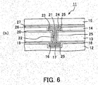
- FIG. 1 is a partial cross section view showing multi-layered interconnection (wiring) at the top layer of a semiconductor device 11 of the present embodiment.
- the semiconductor device 11 comprises a first insulating layer 12, a second insulating layer 13, a third insulating layer 14, and a passivation film 15.
- the first insulating layer 12 comprises a low dielectric constant silicon oxide (SiO 2 ) film, which is formed by having a predetermined porous density.
- the first insulating layer 12 comprises a first groove 16, and a first interconnection (wiring) layer 17 made of copper, is embedded in the first groove 16.
- a film 18 made of silicon nitride (SiN) is provided on the surface of the first insulating layer 12.
- the second insulating layer 13 is placed on the first insulating layer 12.
- the second insulating layer 13 comprises a porous low dielectric constant silicon oxide film.
- the second insulating layer 13 comprises a first and second stopper film 19 and 20 made of SiN, at the surface that contacts the first insulating layer 12 and the surface opposite thereof.
- the first and second stopper films 19 and 20 are provided at a thickness of, for example, 10 to 30nm.
- An interconnection hole 21 is provided penetrating through the second insulating layer 13, which is upwards of the first groove 16.
- a plug layer 22 made of copper is embedded in the interconnection bole 21.
- the third insulating layer 14 is provided on the second insulating layer 13.
- the third insulating layer 14 comprises a porous low dielectric constant silicon oxide film.
- Asecond groove 23 is provided penetrating through the third insulating layer 14, which is on top of the interconnection hole 21.
- a second interconnection layer 24 made of copper is embedded in the second groove 23.
- the multi-layered interconnection layer is formed by the first interconnection layer 17, the plug layer 22, and the second interconnection layer 24.
- a barrier layer 25 is formed in the inner wall of the first groove 16, the interconnection hole 21, and the second groove 23, a barrier layer 25 is formed.
- the barrier layer 25 comprises SiN, and is formed in a thickness of, for example, 5 to 10nm.
- the barrier layer 25 is provided to prevent diffusion of copper, which is the material of interconnection (wiring).
- the first and second stopper films 19, 20 and the barrier layer 25, which are made of SiN, are formed by direct nitriding of the silicon oxide film using an RLSA type plasma processing device, which will be later described.
- An SiN film 26 is provided on the surface of the third insulating layer 14.
- the passivaition film 15 is stacked on the third insulating layer 14, through an SiN film 27.
- the passivation film 15 comprises silicon oxide, and FSG, etc., and functions as an overcoat of the semiconductor device 11.
- the SiN layer 27 that separates the passivation film 15 and the third insualting layer 14, prevents diffusion of copper which is the material of interconnection.
- the plasma processing device used for forming the barrier layer 25 of the above semiconductor device 11 will be described with reference to the drawings.
- the plasma processing device used for forming the barrier layer 25 is an RLSA (Radial Line Slot Antenna) type.
- the plasma processing device generates plasma of the gas to be processed using microwave energy, and modifies the surface of the target to be processed (material including silicon) by the plasma.
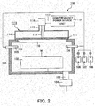
- FIG. 2 shows a cross-sectional structure of a plasma processing device 100.
- the plasma processing device 100 comprises an approximately cylindrical chamber 101.
- the chamber 101 comprises Aluminum, etc.
- a placing base 102 for a semiconductor wafer (hereinafter referred to as wafer W), which is a target to be processed, is placed.
- a temperature controller which is not shown, is embedded in the placing base 102, and the wafer W is heated to a predetermined temperature, for example, room temperature to 600°C, by the temperature controller.
- an exhaust pipe 103 In the bottom part of the chamber 101, one end of an exhaust pipe 103 is connected, and the other end is, connected to an exhaust device 104, such as a vacuum pump, etc.
- the interior of the chamber 101 is set to a predetermined pressure, for example of 4.0Pa to 0.13kPa (30mTorr to 1 Torr), by the exhaust device 104, etc.
- Gas supply lines 105 are provided on the upper side of the chamber 101.
- the gas supply lines 105 are connected to Nitrogen (N 2 ) gas source 106, Hydrogen gas source (H 2 ), and Argon (Ar) gas source 108.
- the gas supply lines 105 are placed evenly spaced apart, for example, in 16 places, in a circumferential direction of the side wall of the chamber 101. By being placed in this way, the gas supplied from the gas supply lines 105 is evenly provided upwards of the wafer W on a placing base 102.
- An opening 109 is provided at the upper part of the chamber 101.
- a window 110 is provided in the inner side of the opening 109.
- the window 110 comprises transmission material, inorganic material such as quartz, SiO 2 glass, Si 3 N 4 , NaCl, KCl, LiF, CaF 2 , BaF 2 , Al 2 O 3 , AlN, and MgO, and a film and a sheet of organic material, such as polyethylene, polyester, polycarbonate, celluloseacetate, polypropylene, polyvinylchloride, polyvinylidenechloride, polystyrene, polyamide, and polyimide.
- inorganic material such as quartz, SiO 2 glass, Si 3 N 4 , NaCl, KCl, LiF, CaF 2 , BaF 2 , Al 2 O 3 , AlN, and MgO
- a film and a sheet of organic material such as polyethylene, polyester, polycarbonate, celluloseacetate, polypropylene, polyvinylchlor
- a radial line slot antenna (hereinafter referred to as RLSA) 111 is provided on the window 110.
- a waveguide 113 connected to a high frequency power source unit 112 is provided on the RLSA 111.
- the waveguide 113 comprises a planiform circular waveguide duct (tube) 114, which the bottom end thereof is connected to the RLSA 111, a cylindrical waveguide duct 115, which one end thereof is connected to the upper surface of the circular waveguide duct 114, a coaxial waveguide modulation 116, which is connected to the upper surface of the cylindrical waveguide duct (tube) 115, and a rectangular waveguide duct (tube) 117, which one end thereof is connected perpendicular to the side surface of the coaxial waveguide modulation 116, and the other end thereof is connected to to the high frequency power source unit 112.
- the RLSA 111 and the waveguide 113 are formed by copper plates.
- a coaxial waveguide duct (tube) 118 is placed in the interior of the circular waveguide duct 114.
- the coaxial waveguide duct 118 is made of axis material, which is made of conducting material, and one end thereof is connected to approximately the center of the upper surface of the RLSA 111, and the other end thereof is connected to the upper surface of the circular waveguide duct 114, on the same axis.
- FIG. 3 shows a plane view of the RLSA 111.
- the RLSA 111 comprises on the surface, a plurality of slots 111a, 111a, ... which are provided concentrically.
- Each slot 111a is an approximately rectangle through hole, and is arranged so that the adjacent slots 111a intersect with each other, to form an approximate alphabet T.
- the length and arrangement interval of the slots 111a are determined according to the wavelength of the radio-frequency wave generated by the high frequency power source unit 112.
- the high frequency power source unit 112 generates a microwave of, for example, 2.45GHz, at an electric power of for eiample 500W to 5kW.
- the microwave generated from the high frequency power source unit 112 is transmitted through the rectangular waveguide duct 117 in a rectangular mode. Furthermore, the microwave is converted to a circular mode from the rectangular mode, in the coaxial waveguide modulation 116, and transferred to the cylindrical waveguide duct 115 in the circular mode.
- the microwave is further transferred in a state, extended in the circular waveguide duct 114, and is emitted by the slots 111a of the RLSA 111.
- the emitted microwave is supplied to the chamber 101, transmitting the window 110.
- High frequency radio wave energy is transmitted to the mixed gas in the chamber 101, and high frequency radio wave plasma is generated.
- the microwave is emitted from the many slots 111a of the RLSA 111, a high density plasma is generated.
- Direct nitriding the surface of the wafer W is carried out by the generated high density plasma.
- nitrogen (N) radical in the generated plasma acts on the surface of the silicon oxide film (SiO 2 film), which is formed on the wafer, and cuts the bond of Si and O and replaces the O to N. In this way, a few nm of the surface of the silicon oxide film is modified to SiN.
- the temperature of the wafer W is room temperature to 600°C, and the pressure in the chamber 101 is 4.0 Pa to 0.13kPa.
- Ar in the mixed gas works as diluted gas, and improves controllability of the reaction.
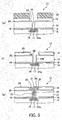
- FIGS. 4 (a) to (d), 5 (e) to (g) and 6 (h) shows the forming process of the interconnection layer of the semiconductor device 11.
- a first insulating layer 12 comprising a first groove 16 in which a first interconnection layer 17 made of copper has been embedded, is prepared.
- the first insulating layer 12 is made of silicon oxide and is provided on the substrate of the semiconductor.
- a barrier layer 25 made of SiN is provided, and on the surface of the first insulating layer 12, an insulating film made of SiN is formed.
- the first groove 16, and the barrier layer 25a, etc., are formed by the latter described Dual-Damascene method.
- a first stopper film 19 made of SiN is formed on the first insulating layer 12 by the CVD method, etc. Furthermore, a second insulating layer 13 made of silicon oxide is formed on the first stopper film 19 by the CVD method, etc. In this case, the thickness of the second insulating layer 13 is set so that it is the height of the interconnection hole 21.
- nitriding is carried out by using an RLSA type plasma processing device 100, and a second stopper film 20 made of SiN is formed on the surface of the second insulating layer 13. Furthermore, as shown in FIG. 4 (c), a third insulating layer 14 made of silicon oxide is formed on the second stopper film 20. In this case, the thickness of the third insulating layer 14 is set so that it is the same height as the second groove 23.
- a resist pattern 30 is formed on the third insulating layer 14, and anisotropic etching is carried out on the condition that etching of the first and second stopper films 19 and 20, and the third insulating layer 14 are carried out at approximately the same speed.
- the etching can be carried out by using for example, mixed gas of CF 4 and O 2 .
- a resist patter 32 is formed on the third insulating layer 14, and the anisotropic etching is carried out on the condition that third insulating layer 14 is etched, but the second stopper film 20 is not.
- the above etching can be carried out by using for example, mixed gas of C 4 F 8 and CO.
- nitrding of the entire surface, including the side walls of the interconnection hole 21 and the second groove 23 is carried out. Nitriding is carried out using the above described RLSA type plasma processing device 100, and a SiN film 33 is formed thinly, on the entire surface of the silicon oxide film.
- the SiN film 33 formed on inner walls of the interconnection hole 21 and the second groove 23 constitutes the barrier layer 25b and the SiN layer 26 for preventing diffusion of the interconnection material.
- a multi-layered interconnection (wiring) layer with two or more layers can be formed.
- an SiN film which prevents diffusion of copper, is formed on the surface of the semiconductor device 11 by CVD, etc.
- a passivation film 15 made of SiO 2 and FSG, etc. is formed on the SiN film by CVD, etc.
- Overcoat such as SiN film, etc., may be further formed on the passivation film 15. In this way, passivation layer is formed on the multi-layered interconnection layer, and the manufacturing process of the semiconductor device 11 is completed.
- the barrier layer 25 that controls the diffusion of interconnection material is formed by direct nitriding of the insulating layer, using the RLSA type plasma processing device 100.
- the barrier layer 25, which is thin and is hard to be peeled off is formed on the side wall of minute interconnection grooves 16, 23, and interconnection hole 21.
- the barrier layer 25 is formed by direct nitriding of the insulating layer, blockage, etc., of the grooves by the formed film does not occur, and the barrier layer 25 can be formed in grooves with a high aspect ratio, without degrading the embedded characteristic.
- first and second stopper films 19 and 20 which are etching stopper films, are formed using the RLSA type plasma processing device 100.
- stopper films which are thin and hard to be peeled off, can be formed in the interlayer dielectric film.
- first and second stopper films 19 and 20 By forming the barrier layer 25, first and second stopper films 19 and 20 by directly nitriding silicon films using the RLSA type plasma processing device 100, a highly reliable semiconductor device 11 can be obtained.
- a nitriding process is carried out at relatively low temperature of room temperature to 600°C. Therefore, the electron temperature of the activated species in the generated plasma is approximately 1.5eV, and low.
- forming of the barrier layer 25 and stopper films 19, 20 can be carried out, controlling the damage to the surface of the film, and preventing degradation of element characteristic due to difference diffusion, etc., of impurities in the element. Therefore, a highly reliable semiconductor device 11, which is prevented degradation of the element characteristic, can be formed.
- the barrier layer 25 is structured by SiN, and not metal materials such as, tantalum nitride, or titanium nitride, etc.
- metal precursor organic metal, etc.
- reaction with the etching residue fluorine, etc.
- destruction of the barrier layer 25, and deterioration of the low dielectric constant film is prevented, and a higher reliability of the semiconductor device 11 can be obtained.
- the RLSA 111 and the waveguide 113 are structured by a copper plate.
- materials such as Al, Cu, and Ag/Cu coated stainless steel, which have a high electric conductivity, can be preferably used as the material which structures the RLSA 111 and the waveguide 113 for controlling propagation loss of microwave.
- the direction of the feed port to the circular waveguide 113 used in the present invention can be a direction of feeding the microwave parallel to the H-plane, such as H-plane T-branch or tangent, or a direction of feeding the microwave orthogonal to the H-plane, such as E-plane T-branch, as long as microwave is effectively fed to the microwave propagation space in the circular waveguide 113.
- the slot interval of the microwave direction is most appropriate at 1/2 or 1/4 the wavelength in the duct.
- high density plasma is generated using a microwave having a wavelength of 2.45GHz.
- microwave frequency can be arbitrarily selected from the range of 0.8GHz to 20 GHz.
- copper is used as material that structures the interconnection.
- metal such as Aluminum or alloyed metal thereof may be used.
- a plug, Tungsten, etc. that is a refractory metal may be used.
- the first, second and third insulating layers 12, 13 and 14 are structured by low dielectric constant silicon oxide films that have a predetermined porous density.
- any kind of insulating film can be used as long as the film having silicon as the main component, and especially having a low dielectric constant.
- a silicon film can be applied to, such as FSG (Fluorinated Silicate Glass), an SiC film, an SiCN film, or an SiOCH film, etc.
- mixed gas of N 2 , H 2 , and Ar is used for directly nitriding the silicon oxide film.
- other gas may be used for nitriding.
- nitrogen included gas such as NH 3 , N 2 O, NO, NO 2 , etc.
- rare gas such as Ne, Xe, and Kr, etc.
- the energy of the activated Ar prevents damage of the film surface, and makes possible activation of silicon (Si), the energy is suitable and preferable.
- reaction conditions such as wafer temperature and reaction pressure, etc., are not limited to the above, and may be of any kind as long as a high quality SiN film can be formed.
- the first and second stopper films 19 and 20 may be formed by CVD, or PVD, etc., instead of the RLSA type plasma processing device 100.
- the stopper films 19 and 20 may be formed SiC, or SiCN, etc., besides SiN.
- the RLSA type plasma processing device 100 used in the present invention may be used as a cluster system, combining a CVD device, an etching device, and a sputtering device for forming seed layers.
- the present invention is applicable in the manufacturing of electronic devices such as semiconductor devices, etc.
Landscapes
- Internal Circuitry In Semiconductor Integrated Circuit Devices (AREA)
- Drying Of Semiconductors (AREA)
- Formation Of Insulating Films (AREA)
Abstract
A hole which is to be a part of an interconnection (wiring) hole (21) is formed
penetrating through a second insulating layer (13) and a third insulating layer (14)
made of porous silicon oxide film, by etching. Further, a second groove (23) is
formed on the third insulating layer (14) using a second stopper film (20), by etching.
Further, direct nitriding of a silicon oxide film applying an RLSA plasma processing
deice is carried out on the side wall of the interconnection hole (21) and the second
groove (23), and a barrier layer (25) made of SiN film is formed. Here, the second
stopper film (20) and the bazrier layer (25) are formed by the same direct nitriding.
Description
The present invention relates to a semiconductor device with a high reliability,
and a manufacturing method thereof.
Speeding up of signal processing is necessary, for achieving high efficiency
of large-scale integration circuits (LSIs). Speeding up of signal processing can be
carried out by miniaturization of circuits and reducing signal delay on interconnection.
In recent years, miniaturizing has progressed, and designing rule of LSI has reached to
0.13 micrometers, and reduction in signal delay on interconnection is especially
important in this kind of LSI.
Reduction in a resistance of interconnections is the effective means for
reducing the above signal delay on interconnections. To reduce in a resistance of
interconnection, copper, which has a high electro-migration tolerance and has a low
resistance, is used instead of aluminum which has been conventionally used.
Because processing of the conventional etching is difficult in a case where copper
interconnection (wiring) is used, the so called Dual Damascene method is used for
realizing multi-layered interconnection, without etching the copper.
A process of manufacturing a semiconductor device 201, which comprises a
multi-layered interconnection layer, using the Dual Damascene method will be
described with reference to FIGS. 7 (a) to (d). First, a cap layer 204 made of silicon
nitride, etc., is formed on a first insulating layer 203 made of silicon oxide, etc., where
an interconnection (wiring) layer 202 is embedded. The interconnection layer 202
surrounds a conductor layer 205 made of copper, and a conductor layer 205, and
comprises a barrier layer 206 made of tantalum nitride, etc. Next, a second
insulating layer 207 made of silicon oxide, etc., is formed on the cap layer 204.
Further, a stopper film 208 made of silicon nitride, etc., is formed on the second
insulating layer 207, and a third insulating layer 209 made of silicon oxide, etc., is
stacked thereon. By this, result abstructures shown in FIG. 7 (a) can be obtained.
Sequentially, as shown in FIG. 7 (b), a resist pattern 210 is formed on the
third insulating layer 209, and a hole 211 having the conductor layer 205 as bottom,
by etching, is formed. At this time, etching is carried out on the condition that the
second and third insulating films 207 and 209, the stopper film 208, and the cap layer
204 are etched. After etching, the resist pattern 210 is removed by ashing, etc.
Sequentially, as shown in FIG. 7 (c), a resists pattern 212 is formed on the
third insulating film 209. And an interconnection groove 213 which overlaps with
the hole 211 and has the stopper film 208 as the bottom, is formed on the third
insulating film 209. By this, the interconnection groove 213, and the interconnection
hole 214 that connects the interconnection groove 213 and the interconnection layer
202 is formed. Here, etching is carried out on the condition that the third insulating
film 209 is etched, but the stopper film 208 is not. Therefore, etching is stopped at
the stopper film 208. After etching, the resist pattern 212 is removed by ashing, etc.
Sequentially, a barrier layer 215 made of tantalum nitride, etc., by CVD, etc.,
to the inner wall of the interconnection groove 213 and the interconnection hole 214,
is formed. Further, after the interior of the interconnection groove 213 and the
interconnection hole 214 are embedded by the plating method, additional copper is
removed by CMP. By the above process, as shown in FIG. 7 (d), a plug layer 216,
and a conductive layer 217 connected to the conductive layer 205 by the plug layer
216 are formed.
In the semiconductor device 201 formed by the above Dual Damascene
method, the barrier layer 215 is provided to prevent diffusion of copper, which is
interconnection material. Because copper is highly diffusive, and is inclined to
deteriorate the characteristic of the semiconductor, the barrier layer 215 is a necessity
in forming interconnection layers made of copper. Especially, in recent years,
because the porous films that are preferably used for the reason that the dielectric
constant is low, has many holes in the interior, copper atoms are likely to penetrate
(diffuse).
The barrier layer 215 is generally structured singularly by metal material such
as titanium nitride, and tantalum nitride, etc., or by being laminated, and is formed by
CVD, etc. However, accompanying the development of miniaturization, if an
interconnection hole 214 such as shown in FIG. 7(c) is further miniaturized, it
becomes difficult to form a highly reliable barrier layer 215 to the entire inner wall of
the interconnection hole 214.
Namely, for example, if the interconnection hole 214 is extremely minute,
infilteration of precursors (organic metal, etc.) of the barrier layer 215 is physically
prevented, and deposition speed in the lower part becomes slower than the upper part
of the interconnection hole 214. By this a barrier layer 215 with enough thickness is
not formed in the lower part of the interconnection hole 214, and barrier characteristic
deteriorates. Further, if the barrier layer 215 is uneven, void becomes likely to occur
in the latter copper embedding process.
At this time, in a case where porous insulating films are used as interlayer
dielectric films 207 and 209, precursors infilterate through the hole in the insulation
film, when forming the barrier-layer 215 by CVD. These react with etching gas at
the time of etching, and leads to deterioration of the insulating film.
Accompanying miniaturization, the thickness of the barrier layer 215
becomes thinner, and the adhesiveness to the surface of the interconnection groove
213 and the interconnection hole 214 is deteriorated. By this, peeling off, etc., of the
barrier layer 215 becomes likely to occur, and reliability of the barrier layer 215 and
the semiconductor device 201 degrades. In this way, it is difficult to form a highly
reliable barrier layer at the inner wall of a highly miniaturized (with a high aspect
ratio) groove or hole.
On the other hand, as described above, in the Dual Damascene method, the
stopper film 208 of etching is used. As shown in FIG. 7 (d), the stopper film 208
forms the bottom part of the interconnection groove 213. Accompanying the
progress of miniaturization, thinning of the stopper film 208 is also being sought.
Therefore, in the same way as the above barrier layer 215, in a case where a thin film
stopper film 208 formed by CVD, etc., is used, adhesiveness with the second
insulating film 207 deteriorates, and peeling off becomes likely to occur. In the case
where the stopper film 208 is peeled off, etc., the barrier layer 215 stacked thereon
becomes uneven, and lowly reliable.
In this way, it is hard to form highly reliable barrier layers and stopper films
by conventional PVD or CVD, on the inner wall of the miniaturized interconnection
grooves and interconnection holes, and there was a risk of deteriorating the reliability
of the semiconductor device, by the diffusion, etc., of interconnection material.
In consideration of the above, an object of the present invention is to provide
a highly reliable semiconductor device and manufacturing method thereof.
Another object of the present invention is to provide a semiconductor device
which comprises a highly reliable barrier layer, and manufacturing method thereof.
Still another object of the present invention is to provide a semiconductor
device which comprises a highly reliable stopper film, and manufacturing method
thereof.
To achieve the above objects, a manufacturing method of a semiconductor
device according to a first aspect is characterized by comprising:
In the above structure, a barrier layer made of silicon nitride film is formed at
the inner wall of an interconnection groove and an interconnection hole, where
interconnection material (especially copper) is embedded. Silicon nitride film that
constitutes the barrier layer is formed by reforming the surface region of the insulating
layers made of a film including silicon, by plasma of nitrogen gas. In this way, by
directly reforming the surface of the insulating layers, a thin barrier layer can be
formed with a high reliability at the inner wall of a groove and hole, which is minute
and has a high aspect ratio. By this, a highly reliable semiconductor device where
diffusion of interconnection material is reduced, can be provided.
In the above structure, it is preferable that the barrier layer forming step
comprises a step of nitriding the surface region of the groove and the hole by exposing
the surface of the inner wall of the groove and the hole to the plasma of gas including
nitrogen. In this way, by forming the barrier layer by direct nitriding of the
insulating layers, a thin barrier layer with little peeling off, etc., can be formed.
In the above structure, it is preferable that the plasma of gas including nitrogen
is generated by irradiating microwave from a plane antenna that comprises a plurality
of slits to gas including nitrogen. By this, a thin barrier layer can be formed,
reducing plasma damage provided to other film surfaces.
In the above structure, the insulating layers may be structured by porous
dielectric film. In the forming of the barrier layer, metal precursor such as organic
metal, etc., are not used, and even in a case where a porous dielectric film is used to
the insulating layers, metal precursors, etc., do not enter the hole in the insulating
layers. By this, deterioration of insulating layers occurred by reaction, etc., of metal
precursors and etching gas in the hole is prevented, and a highly reliable
semiconductor device can be obtained.
To achieve the above objects, a manufacturing method of a semiconductor
device according to a second aspect is characterized by comprising:
According to the above structure, the stopper film made of silicon nitride film
is formed by surface modification by plasma. The formed stopper film is a film with
little plasma damage on the surface and of high quality. By this, the stopper film that
comprises the bottom part of the interconnection groove can be formed with at high
reliability.
In the above structure, it is preferable that the step of forming the stopper film
comprises a step of nitriding the surface region of the first insulating layer by
exposing the surface of the first insulating layer to the plasma of gas including
nitrogen. In this way, by forming the stopper film by direct nitriding of the
insulating films, a thin stopper film with little peeling off, can be formed controlling
surface damage.
In the above structure, the first and second insulating layers may be structured
by porous dielectric film.
In the above structure, copper may be used as the main component, as the
conductive material. Namely, the silicon nitride film has barrier characteristics
towards copper, and functions effectively as the barrier layer.
In the above structure, gas including hydrogen may be further used as the
above gas. By this, at the same time as the forming of the silicon nitride film,
hydrogen can be combined with the dangling bond of silicon that exists at the surface
region of the insulating layers, so that the film can be stabilized.
In the above structure, it is preferable that the forming of the barrier layer is
carried out at room temperature to 600°C. By carrying out processing at a relatively
low temperature, diffusion of impurities can be preverited, and deterioration of device
characteristic can be prevented.
In the above structure, the barrier layer may be formed in a thickness of 1nm
to 20nm. Also, the stopper film may be formed in a thickness of 1nm to 20nm.
To achieve the above objects, a semiconductor device according to a third
aspect of the present invention is characterized by comprising:
According to the above structure, by applying silicon nitride film as the
barrier layer, substantially, metal precursors do not enter the hole in the insulating
layers at the time of forming the barrier film, as in the case of forming a barrier film
including metal. Therefore, destruction and deterioration of insulating layers after
processes of etching, etc., can be prevented, and a highly reliable semiconductor
device can be obtained.
To achieve the above objects, a semiconductor device according to a fourth
aspect of the present invention is characterized by comprising:
In the above structure, a barrier layer made of silicon nitride film is formed at
the inner wall of an interconnection groove and an interconnection hole, where
interconnection material (especially copper) is embedded. A silicon nitride film that
constitutes the barrier layer is formed in the surface region of the insulating layers
made of a film including silicon by microwave plasma applying radial line slot
antenna (RLSA). In this way, by applying RLSA plasma, a thin barrier layer can be
formed with a high reliability at the inner wall of a groove and hole, which is minute
and has a high aspect ratio. By this, a highly reliable semiconductor device where
diffusion of interconnection material is reduced can be provided.
To achieve the above objects, a semiconductor device according to a fifth
aspect of the present invention is characterized by comprising:
According to the above structure, the stopper film made of silicon nitride
film is formed by RLSA plasma. The stopper film formed by RLSA plasma is a high
quality film with little damage on the surface. By this, the stopper film that
structures the bottom part of the interconnection groove can be formed with high
reliability.
A semiconductor device according to the present embodiment will be
described with reference to the drawings. The semiconductor device of the present
embodiment comprises a transistor that is provided on a semiconductor substrate,
elements such as a memory, etc., and a multi-layered interconnection (wiring) layer
connected thereto.
FIG. 1 is a partial cross section view showing multi-layered interconnection
(wiring) at the top layer of a semiconductor device 11 of the present embodiment.
As shown in FIG. 1, the semiconductor device 11 comprises a first insulating layer 12,
a second insulating layer 13, a third insulating layer 14, and a passivation film 15.
The first insulating layer 12 comprises a low dielectric constant silicon oxide
(SiO2) film, which is formed by having a predetermined porous density. The first
insulating layer 12 comprises a first groove 16, and a first interconnection (wiring)
layer 17 made of copper, is embedded in the first groove 16. A film 18 made of
silicon nitride (SiN) is provided on the surface of the first insulating layer 12.
The second insulating layer 13 is placed on the first insulating layer 12. The
second insulating layer 13 comprises a porous low dielectric constant silicon oxide
film. The second insulating layer 13 comprises a first and second stopper film 19
and 20 made of SiN, at the surface that contacts the first insulating layer 12 and the
surface opposite thereof. The first and second stopper films 19 and 20 are provided
at a thickness of, for example, 10 to 30nm.
An interconnection hole 21 is provided penetrating through the second
insulating layer 13, which is upwards of the first groove 16. A plug layer 22 made of
copper is embedded in the interconnection bole 21.
The third insulating layer 14 is provided on the second insulating layer 13.
The third insulating layer 14 comprises a porous low dielectric constant silicon oxide
film. Asecond groove 23 is provided penetrating through the third insulating layer
14, which is on top of the interconnection hole 21. A second interconnection layer
24 made of copper is embedded in the second groove 23.
In this way, the multi-layered interconnection layer is formed by the first
interconnection layer 17, the plug layer 22, and the second interconnection layer 24.
In the inner wall of the first groove 16, the interconnection hole 21, and the second
groove 23, a barrier layer 25 is formed. The barrier layer 25 comprises SiN, and is
formed in a thickness of, for example, 5 to 10nm. The barrier layer 25 is provided to
prevent diffusion of copper, which is the material of interconnection (wiring).
Here, the first and second stopper films 19, 20 and the barrier layer 25, which
are made of SiN, are formed by direct nitriding of the silicon oxide film using an
RLSA type plasma processing device, which will be later described.
An SiN film 26 is provided on the surface of the third insulating layer 14.
The passivaition film 15 is stacked on the third insulating layer 14, through an SiN
film 27. The passivation film 15 comprises silicon oxide, and FSG, etc., and
functions as an overcoat of the semiconductor device 11. The SiN layer 27 that
separates the passivation film 15 and the third insualting layer 14, prevents diffusion
of copper which is the material of interconnection.
A plasma processing device used for forming the barrier layer 25 of the above
semiconductor device 11 will be described with reference to the drawings. The
plasma processing device used for forming the barrier layer 25 is an RLSA (Radial
Line Slot Antenna) type. The plasma processing device generates plasma of the gas
to be processed using microwave energy, and modifies the surface of the target to be
processed (material including silicon) by the plasma.
FIG. 2 shows a cross-sectional structure of a plasma processing device 100.
As shown in FIG. 2, the plasma processing device 100 comprises an approximately
cylindrical chamber 101. The chamber 101 comprises Aluminum, etc.
In the center of the chamber 101, a placing base 102 for a semiconductor
wafer (hereinafter referred to as wafer W), which is a target to be processed, is placed.
A temperature controller, which is not shown, is embedded in the placing base 102,
and the wafer W is heated to a predetermined temperature, for example, room
temperature to 600°C, by the temperature controller.
In the bottom part of the chamber 101, one end of an exhaust pipe 103 is
connected, and the other end is, connected to an exhaust device 104, such as a vacuum
pump, etc. The interior of the chamber 101 is set to a predetermined pressure, for
example of 4.0Pa to 0.13kPa (30mTorr to 1 Torr), by the exhaust device 104, etc.
An opening 109 is provided at the upper part of the chamber 101. A
window 110 is provided in the inner side of the opening 109. The window 110
comprises transmission material, inorganic material such as quartz, SiO2 glass, Si3N4,
NaCl, KCl, LiF, CaF2, BaF2, Al2O3, AlN, and MgO, and a film and a sheet of organic
material, such as polyethylene, polyester, polycarbonate, celluloseacetate,
polypropylene, polyvinylchloride, polyvinylidenechloride, polystyrene, polyamide,
and polyimide.
For example, a radial line slot antenna (hereinafter referred to as RLSA) 111
is provided on the window 110. A waveguide 113 connected to a high frequency
power source unit 112 is provided on the RLSA 111. The waveguide 113 comprises
a planiform circular waveguide duct (tube) 114, which the bottom end thereof is
connected to the RLSA 111, a cylindrical waveguide duct 115, which one end thereof
is connected to the upper surface of the circular waveguide duct 114, a coaxial
waveguide modulation 116, which is connected to the upper surface of the cylindrical
waveguide duct (tube) 115, and a rectangular waveguide duct (tube) 117, which one
end thereof is connected perpendicular to the side surface of the coaxial waveguide
modulation 116, and the other end thereof is connected to to the high frequency power
source unit 112. The RLSA 111 and the waveguide 113 are formed by copper plates.
In the interior of the circular waveguide duct 114, a coaxial waveguide duct
(tube) 118 is placed. The coaxial waveguide duct 118 is made of axis material,
which is made of conducting material, and one end thereof is connected to
approximately the center of the upper surface of the RLSA 111, and the other end
thereof is connected to the upper surface of the circular waveguide duct 114, on the
same axis.
FIG. 3 shows a plane view of the RLSA 111. As shown in FIG. 3, the
RLSA 111 comprises on the surface, a plurality of slots 111a, 111a, ... which are
provided concentrically. Each slot 111a is an approximately rectangle through hole,
and is arranged so that the adjacent slots 111a intersect with each other, to form an
approximate alphabet T. The length and arrangement interval of the slots 111a are
determined according to the wavelength of the radio-frequency wave generated by the
high frequency power source unit 112.
The high frequency power source unit 112 generates a microwave of, for
example, 2.45GHz, at an electric power of for eiample 500W to 5kW. The
microwave generated from the high frequency power source unit 112 is transmitted
through the rectangular waveguide duct 117 in a rectangular mode. Furthermore, the
microwave is converted to a circular mode from the rectangular mode, in the coaxial
waveguide modulation 116, and transferred to the cylindrical waveguide duct 115 in
the circular mode. The microwave is further transferred in a state, extended in the
circular waveguide duct 114, and is emitted by the slots 111a of the RLSA 111. The
emitted microwave is supplied to the chamber 101, transmitting the window 110.
The interior of the chamber 101 is set at a predetermined vacuum pressure,
and mixed gas of Ar, N2, and H2 is supplied to the interior of the chamber through a
gas supply lines 105, at for example, Ar/ N2/ H2/ = 10: 1: 1. High frequency radio
wave energy is transmitted to the mixed gas in the chamber 101, and high frequency
radio wave plasma is generated. At this time, because the microwave is emitted from
the many slots 111a of the RLSA 111, a high density plasma is generated.
Direct nitriding the surface of the wafer W is carried out by the generated
high density plasma. Namely, nitrogen (N) radical in the generated plasma, acts on
the surface of the silicon oxide film (SiO2 film), which is formed on the wafer, and
cuts the bond of Si and O and replaces the O to N. In this way, a few nm of the
surface of the silicon oxide film is modified to SiN. At this time, the temperature of
the wafer W is room temperature to 600°C, and the pressure in the chamber 101 is 4.0
Pa to 0.13kPa.
At this time, Ar in the mixed gas, works as diluted gas, and improves
controllability of the reaction. The H radical generated from H2 bonds with the
dangling bond of Si, and stabilizes the SiN film formed by modifying, and improves
the film quality.
Manufacturing method of the above described semiconductor device 11 will
be described with reference to the drawings. In the present embodiment, a
semiconductor device 11 comprising a barrier layer 25 is manufactured by the
Dual-Damascene method. FIGS. 4 (a) to (d), 5 (e) to (g) and 6 (h) shows the forming
process of the interconnection layer of the semiconductor device 11.
First, a first insulating layer 12, comprising a first groove 16 in which a first
interconnection layer 17 made of copper has been embedded, is prepared. The first
insulating layer 12 is made of silicon oxide and is provided on the substrate of the
semiconductor. In the circumference of the first groove 16, a barrier layer 25 made
of SiN is provided, and on the surface of the first insulating layer 12, an insulating
film made of SiN is formed. The first groove 16, and the barrier layer 25a, etc., are
formed by the latter described Dual-Damascene method.
Next, as shown in FIG. 4 (a), a first stopper film 19 made of SiN is formed on
the first insulating layer 12 by the CVD method, etc. Furthermore, a second
insulating layer 13 made of silicon oxide is formed on the first stopper film 19 by the
CVD method, etc. In this case, the thickness of the second insulating layer 13 is set
so that it is the height of the interconnection hole 21.
Sequentially, as shown in FIG. 4 (b), nitriding is carried out by using an
RLSA type plasma processing device 100, and a second stopper film 20 made of SiN
is formed on the surface of the second insulating layer 13. Furthermore, as shown in
FIG. 4 (c), a third insulating layer 14 made of silicon oxide is formed on the second
stopper film 20. In this case, the thickness of the third insulating layer 14 is set so
that it is the same height as the second groove 23.
Then, as shown in FIG. 4 (d), a resist pattern 30 is formed on the third
insulating layer 14, and anisotropic etching is carried out on the condition that etching
of the first and second stopper films 19 and 20, and the third insulating layer 14 are
carried out at approximately the same speed. The etching can be carried out by using
for example, mixed gas of CF4 and O2. By etching the resist pattern 30, the hole 31
that structures the interconnection hole 21 is formed.
After the resist pattern 30 is removed by ashing, etc., as shown in FIG. 5 (e),
a resist patter 32 is formed on the third insulating layer 14, and the anisotropic etching
is carried out on the condition that third insulating layer 14 is etched, but the second
stopper film 20 is not. The above etching can be carried out by using for example,
mixed gas of C4F8 and CO. By the etching using the resist pattern 32, the second
groove 23 is formed.
After the resist pattern 32 is removed by ashing, etc., as shown in FIG. 5 (f),
nitrding of the entire surface, including the side walls of the interconnection hole 21
and the second groove 23 is carried out. Nitriding is carried out using the above
described RLSA type plasma processing device 100, and a SiN film 33 is formed
thinly, on the entire surface of the silicon oxide film. The SiN film 33 formed on
inner walls of the interconnection hole 21 and the second groove 23 constitutes the
barrier layer 25b and the SiN layer 26 for preventing diffusion of the interconnection
material.
Sequentially, plating of copper is carried, after a seed layer made of copper is
thinly formed by PVD, etc. After the interior of the interconnection hole 21 and the
groove 23 is completely embedded by plating copper, an unnecessary metal film at the
top surface is removed by CMP (Chemical Mechanical Polishing). By this, as shown
in FIG. 5 (g), a double layer interconnect, where the first interconnection layer 17 and
the second interconnection layer 24 are connected by the plug layer 22, is formed.
By repeating the above process predetermined times, a multi-layered
interconnection (wiring) layer with two or more layers can be formed.
Finally, an SiN film, which prevents diffusion of copper, is formed on the
surface of the semiconductor device 11 by CVD, etc. Then, as shown in FIG. 6 (h), a
passivation film 15 made of SiO2 and FSG, etc., is formed on the SiN film by CVD,
etc. Overcoat such as SiN film, etc., may be further formed on the passivation film
15. In this way, passivation layer is formed on the multi-layered interconnection
layer, and the manufacturing process of the semiconductor device 11 is completed.
As described above, in the semiconductor device 11 of the above embodiment,
the barrier layer 25 that controls the diffusion of interconnection material is formed by
direct nitriding of the insulating layer, using the RLSA type plasma processing device
100. By this, the barrier layer 25, which is thin and is hard to be peeled off is formed
on the side wall of minute interconnection grooves 16, 23, and interconnection hole 21.
Furthermore, because the barrier layer 25 is formed by direct nitriding of the
insulating layer, blockage, etc., of the grooves by the formed film does not occur, and
the barrier layer 25 can be formed in grooves with a high aspect ratio, without
degrading the embedded characteristic.
In the same way, first and second stopper films 19 and 20, which are etching
stopper films, are formed using the RLSA type plasma processing device 100. By
this, stopper films, which are thin and hard to be peeled off, can be formed in the
interlayer dielectric film.
By forming the barrier layer 25, first and second stopper films 19 and 20 by
directly nitriding silicon films using the RLSA type plasma processing device 100, a
highly reliable semiconductor device 11 can be obtained.
In the RLSA type plasma processing device 100, a nitriding process is carried
out at relatively low temperature of room temperature to 600°C. Therefore, the
electron temperature of the activated species in the generated plasma is approximately
1.5eV, and low. By this, forming of the barrier layer 25 and stopper films 19, 20 can
be carried out, controlling the damage to the surface of the film, and preventing
degradation of element characteristic due to difference diffusion, etc., of impurities in
the element. Therefore, a highly reliable semiconductor device 11, which is
prevented degradation of the element characteristic, can be formed.
Furthermore, the barrier layer 25 is structured by SiN, and not metal materials
such as, tantalum nitride, or titanium nitride, etc. By this, substantially, there is no
infilteration of metal precursor (organic metal, etc.) to the porous silicon oxide films
13 and 14, and reaction with the etching residue (fluorine, etc.), which is infilterated to
the interior of the insulating film at the time of etching, can be prevented. By this,
destruction of the barrier layer 25, and deterioration of the low dielectric constant film
is prevented, and a higher reliability of the semiconductor device 11 can be obtained.
The present invention is not limited to the above embodiment, and various
modifications and applications are possible. Below, an applicable modification mode
of the above embodiment will be described.
In the above embodiment, the RLSA 111 and the waveguide 113 are
structured by a copper plate. Here, materials such as Al, Cu, and Ag/Cu coated
stainless steel, which have a high electric conductivity, can be preferably used as the
material which structures the RLSA 111 and the waveguide 113 for controlling
propagation loss of microwave.
The direction of the feed port to the circular waveguide 113 used in the
present invention, can be a direction of feeding the microwave parallel to the H-plane,
such as H-plane T-branch or tangent, or a direction of feeding the microwave
orthogonal to the H-plane, such as E-plane T-branch, as long as microwave is
effectively fed to the microwave propagation space in the circular waveguide 113.
The slot interval of the microwave direction is most appropriate at 1/2 or 1/4 the
wavelength in the duct.
In the above embodiment, high density plasma is generated using a
microwave having a wavelength of 2.45GHz. However, it is not limited to this, and
microwave frequency can be arbitrarily selected from the range of 0.8GHz to 20 GHz.
In the above embodiment, copper is used as material that structures the
interconnection. However it is not limited to copper, and metal such as Aluminum
or alloyed metal thereof may be used. Especially, as a plug, Tungsten, etc., that is a
refractory metal may be used.
In the above embodiment, the first, second and third insulating layers 12, 13
and 14, are structured by low dielectric constant silicon oxide films that have a
predetermined porous density. However, it is not limited to this, in the present
invention, any kind of insulating film can be used as long as the film having silicon as
the main component, and especially having a low dielectric constant. For example,
in the present invention, a silicon film can be applied to, such as FSG (Fluorinated
Silicate Glass), an SiC film, an SiCN film, or an SiOCH film, etc.
In the above embodiment, mixed gas of N2, H2, and Ar is used for directly
nitriding the silicon oxide film. However, other gas may be used for nitriding. For
example nitrogen included gas such as NH3, N2O, NO, NO2, etc., can be used instead
of N2, and rare gas such as Ne, Xe, and Kr, etc., can be used instead of Ar. However,
because the energy of the activated Ar prevents damage of the film surface, and makes
possible activation of silicon (Si), the energy is suitable and preferable.
The mixing ratio of the above mixed gas is not limited to the above (Ar/N2/H2
= 10: 1: 1), and the abundance ratio of N2 and H2 can be changed in the range of for
example, 0.05 to 5. Furthermore, reaction conditions such as wafer temperature and
reaction pressure, etc., are not limited to the above, and may be of any kind as long as
a high quality SiN film can be formed.
In the above semiconductor device 11, the first and second stopper films 19
and 20 may be formed by CVD, or PVD, etc., instead of the RLSA type plasma
processing device 100. In this case, the stopper films 19 and 20 may be formed SiC,
or SiCN, etc., besides SiN. However, from the point of productivity, it is preferable
to form the barrier layer 25 and first and second stopper films 19 and 20 by the RLSA
type plasma processing device 100.
The RLSA type plasma processing device 100 used in the present invention
may be used as a cluster system, combining a CVD device, an etching device, and a
sputtering device for forming seed layers.
As described above according to the present invention, a highly reliable
semiconductor device, and manufacturing method thereof is provided.
The present invention is applicable in the manufacturing of electronic devices
such as semiconductor devices, etc.
The patent application is based on Japanese Patent Application No. 2001-260181
filed with the Japan Patent Office on August 29, 2001, and including claims, drawings
and summary, the entire disclosure of which is hereby incorporated by reference.
Claims (21)
- A manufacturing method of a semiconductor device (11) characterized by comprising:a step of forming insulating layers (13, 14) that are structured by silicon as the main component, and comprises a groove (23) at one side, and a hole (21) that penetrates from the bottom part of said groove (23) to the other side;a barrier layer forming step of exposing the surface of the inner wall of said groove (23) and said hole (21) to the plasma of gas including nitrogen, and forming a barrier layer (25) that is structured by silicon nitride film, on the surface region of the inner wall of the groove (23) and the hole (21);a step of embedding an interconnection (wiring) layer (24) made of conductive material, to the inner side of the groove (23) and the hole (21) through the barrier layer (25).
- The manufacturing method of the semiconductor device (11) according to claim 1, characterized in that the barrier layer forming step comprises nitriding the surface region of the groove (23) and the hole (21) by exposing the surface of the inner wall of the groove (23) and the hole (21) to the plasma of gas including nitrogen.
- The manufacturing method of the semiconductor device (11) according to claim 1, characterized in that said plasma of gas including nitrogen is generated by irradiating microwave from a plane antenna (111) that comprises a plurality of slits (111a).
- The manufacturing method of the semiconductor device (11) according to claim 1, characterized in that said insulating layers (13, 14) are structured by porous dielectric films.
- A manufacturing method of a semiconductor device (11) characterized by comprising:a step of forming a first insulating layer (13) structured by silicon as the main component,a step of exposing the surface of the insulating layer (13) to the plasma of gas including nitrogen, and forming a stopper film (20) that is structured by a silicon nitride film, on the surface region of the first insulating layer (13);a step of forming a second insulating layer (14) on the stopper film (20);a step of forming a hole (31) that penetrates the first insulating layer (13) and the second insulating layer (14);a step of forming a hole or groove (23) that overlaps with said hole (31) in said second insulating layer (14), using said stopper film (20) as an etching stopper.
- The manufacturing method of the semiconductor device (11) according to claim 5, characterized in that the step of forming said stopper film (20) comprises nitriding the surface region of the first insulating layer (13) by exposing the surface of the first insulating layer (13) to the plasma of gas including nitrogen.
- The manufacturing method of the semiconductor device (11) according to claim 5, characterized in that the plasma of gas including nitrogen is generated by irradiating microwave from a plane antenna (111) comprising a plurality of slits (111a) to the gas including nitrogen.
- The manufacturing method of the semiconductor device (11) according to claim 5, characterized in that the first and second insulating layers (13, 14) are structured by porous dielectric films.
- The manufacturing method of the semiconductor device (11) according to claim 1, characterized in that copper is used as the main component, for said conductive material.
- The manufacturing method of the semiconductor device (11) according to claim 5, characterized in that copper is used as the main component, for said conductive material.
- The manufacturing method of the semiconductor device (11) according to claim 1, characterized in that gas including hydrogen is further used as said gas.
- The manufacturing method of the semiconductor device (11) according to claim 5, characterized in that gas including hydrogen is further used as said gas.
- The manufacturing method of the semiconductor device (11) according to claim 1, characterized in that the forming of said barrier layer (25) is carried out at room temperature to 600°C.
- The manufacturing method of the semiconductor device (11) according to claim 5, characterized in that the forming of said barrier layer (25) is carried out at room temperature to 600°C.
- The manufacturing method of the semiconductor device (11) according to claim 1, characterized in that the barrier layer (25) is formed in a thickness of 1nm to 20nm.
- The manufacturing method of the semiconductor device (11) according to claim 5, characterized un that the barrier layer (25) is formed in a thickness of 1nm to 20nm.
- The manufacturing method of the semiconductor device (11) according to claim 1, characterized in that the stopper film (20) is formed in a thickness of 1nm to 20nm.
- The manufacturing method of the semiconductor device (11) according to claim 5, characterized in that the stopper film (20) is formed in a thickness of 1nm to 20nm.
- A semiconductor device (11) characterized by comprising:insulating layers (13, 14) that are structured by silicon as the main component, and comprise a groove (23) at one side, and a hole (21) that penetrates from the bottom part of said groove (23) to the other side;an interconnection layer (24), which is embedded in said groove (23) and said hole (21), and is made of conductive material; anda barrier layer (25) which comprises a silicon nitride film, and is provided at the interface with the insulating layers (13, 14) and the interconnection layer (24), and which prevents diffusion of said conductive material, to said insulating layers (13, 14).
- A semiconductor device (11) characterized by comprising:insulating layers (13, 14) that are structured by silicon as the main component, and comprise a groove (23) at one side, and a hole (21) that penetrates from the bottom part of said groove (23) to the other side;an interconnection layer (24), which is embedded in said groove (23) and said hole (21), and is made of conductive material,a barrier layer (25) which is provided at the interface with the insulating layers (13, 14) and the interconnection layer (24), and which prevents diffusion of said conductive material, to said insulating layers (13, 14); whereinsaid barrier layer (25) is formed by exposing the surface of the insulating layers (13, 14) to the plasma generated by irradiating microwave to gas that includes nitrogen from a plane antenna (111) that comprises a plurality of slits (111a), and forming a silicon nitride film on the surface region of the insulating layers (13, 14).
- A semiconductor device (11) characterized by comprising:a first insulating layer (13) which comprises a hole (21) and which is structured by silicon as the main component;a stopper film (20) provided on the first insulating layer (13), and comprises an opening that overlaps with said hole (21);a second insulating layer (14) which is provided on the stopper film (20), and comprises a hole or groove (23) that overlaps with the opening, and has a larger diameter than said opening; whereinsaid stopper film (20) is formed by exposing one surface of the first insulating layer (13) to the plasma of gas including nitrogen, which is generated by irradiating microwave to the gas including nitrogen, from a plane antenna (111) comprising a plurality of slits (111a), and forming a silicon nitride film on the surface region.
Applications Claiming Priority (3)
| Application Number | Priority Date | Filing Date | Title |
|---|---|---|---|
| JP2001260181 | 2001-08-29 | ||
| JP2001260181A JP2003068850A (en) | 2001-08-29 | 2001-08-29 | Semiconductor device and method of manufacturing the same |
| PCT/JP2002/008737 WO2003019650A1 (en) | 2001-08-29 | 2002-08-29 | Semiconductor device and production method therefor |
Publications (2)
| Publication Number | Publication Date |
|---|---|
| EP1432023A1 true EP1432023A1 (en) | 2004-06-23 |
| EP1432023A4 EP1432023A4 (en) | 2005-12-28 |
Family
ID=19087421
Family Applications (1)
| Application Number | Title | Priority Date | Filing Date |
|---|---|---|---|
| EP02770176A Ceased EP1432023A4 (en) | 2001-08-29 | 2002-08-29 | SEMICONDUCTOR DEVICE AND METHOD FOR PRODUCING THE SAME |
Country Status (7)
| Country | Link |
|---|---|
| US (1) | US20050003660A1 (en) |
| EP (1) | EP1432023A4 (en) |
| JP (1) | JP2003068850A (en) |
| KR (1) | KR100619470B1 (en) |
| CN (2) | CN100365796C (en) |
| TW (2) | TWI297518B (en) |
| WO (1) | WO2003019650A1 (en) |
Cited By (1)
| Publication number | Priority date | Publication date | Assignee | Title |
|---|---|---|---|---|
| EP1898456A4 (en) * | 2005-06-08 | 2009-11-18 | Univ Tohoku | PLASMA NITRURATION METHOD, SEMICONDUCTOR DEVICE MANUFACTURING METHOD, AND PLASMA PROCESSING APPARATUS |
Families Citing this family (27)
| Publication number | Priority date | Publication date | Assignee | Title |
|---|---|---|---|---|
| TWI225668B (en) | 2002-05-13 | 2004-12-21 | Tokyo Electron Ltd | Substrate processing method |
| JP4256340B2 (en) * | 2002-05-16 | 2009-04-22 | 東京エレクトロン株式会社 | Substrate processing method |
| WO2004107434A1 (en) | 2003-05-29 | 2004-12-09 | Nec Corporation | Wiring structure and method for producing same |
| JP4358563B2 (en) * | 2003-07-02 | 2009-11-04 | 東京エレクトロン株式会社 | Method for forming low dielectric constant insulating film of semiconductor device |
| JP2005183567A (en) * | 2003-12-18 | 2005-07-07 | Matsushita Electric Ind Co Ltd | Semiconductor integrated circuit manufacturing method, via hole forming shared mask, and semiconductor integrated circuit |
| JP2005203476A (en) * | 2004-01-14 | 2005-07-28 | Oki Electric Ind Co Ltd | Wiring structure of semiconductor device and manufacturing method thereof |
| JP2005217371A (en) * | 2004-02-02 | 2005-08-11 | Matsushita Electric Ind Co Ltd | Semiconductor device and manufacturing method thereof |
| CN1787186A (en) | 2004-12-09 | 2006-06-14 | 富士通株式会社 | Semiconductor device fabrication method |
| JP2006253666A (en) * | 2005-02-10 | 2006-09-21 | Nec Electronics Corp | Semiconductor device and manufacturing method thereof |
| JP4540504B2 (en) * | 2005-03-03 | 2010-09-08 | 富士通セミコンダクター株式会社 | Manufacturing method of semiconductor device |
| WO2006126536A1 (en) * | 2005-05-25 | 2006-11-30 | Nec Corporation | Semiconductor device and method for fabricating the same |
| KR100731496B1 (en) * | 2006-08-31 | 2007-06-21 | 동부일렉트로닉스 주식회사 | Semiconductor device and manufacturing method |
| JP2008270706A (en) * | 2007-03-26 | 2008-11-06 | Tokyo Electron Ltd | Silicon nitride film and nonvolatile semiconductor memory device |
| JP5366235B2 (en) * | 2008-01-28 | 2013-12-11 | 東京エレクトロン株式会社 | Semiconductor device manufacturing method, semiconductor manufacturing apparatus, and storage medium |
| US8847186B2 (en) | 2009-12-31 | 2014-09-30 | Micron Technology, Inc. | Self-selecting PCM device not requiring a dedicated selector transistor |
| GB201110117D0 (en) * | 2011-06-16 | 2011-07-27 | Fujifilm Mfg Europe Bv | method and device for manufacturing a barrie layer on a flexible substrate |
| US9111772B1 (en) * | 2014-01-29 | 2015-08-18 | Infineon Technologies Ag | Electronic array and chip package |
| CN105336576A (en) * | 2014-08-12 | 2016-02-17 | 中芯国际集成电路制造(上海)有限公司 | Semiconductor device and fabrication method thereof |
| US10211148B2 (en) | 2015-12-14 | 2019-02-19 | International Business Machines Corporation | Structural enhancement of Cu nanowires |
| US9786603B1 (en) | 2016-09-22 | 2017-10-10 | International Business Machines Corporation | Surface nitridation in metal interconnects |
| US9741609B1 (en) | 2016-11-01 | 2017-08-22 | International Business Machines Corporation | Middle of line cobalt interconnection |
| KR101808605B1 (en) * | 2016-12-22 | 2018-01-18 | 김재범 | Non-conductive frame coated with conductive layer transmitting the electormagnetic wave or having the function of heat radiation |
| US11133216B2 (en) | 2018-06-01 | 2021-09-28 | International Business Machines Corporation | Interconnect structure |
| US11049731B2 (en) * | 2018-09-27 | 2021-06-29 | Applied Materials, Inc. | Methods for film modification |
| JP2020155591A (en) | 2019-03-20 | 2020-09-24 | 株式会社東芝 | Semiconductor device |
| US11227792B2 (en) * | 2019-09-19 | 2022-01-18 | International Business Machines Corporation | Interconnect structures including self aligned vias |
| US12315807B2 (en) | 2021-12-31 | 2025-05-27 | International Business Machines Corporation | Reducing copper line resistance |
Family Cites Families (11)
| Publication number | Priority date | Publication date | Assignee | Title |
|---|---|---|---|---|
| JP3297220B2 (en) * | 1993-10-29 | 2002-07-02 | 株式会社東芝 | Semiconductor device manufacturing method and semiconductor device |
| JPH11145138A (en) * | 1997-11-10 | 1999-05-28 | Hitachi Ltd | Semiconductor device and manufacturing method thereof |
| US6140024A (en) * | 1997-12-31 | 2000-10-31 | Texas Instruments Incorporated | Remote plasma nitridation for contact etch stop |
| US6252303B1 (en) * | 1998-12-02 | 2001-06-26 | Advanced Micro Devices, Inc. | Intergration of low-K SiOF as inter-layer dielectric |
| JP4255563B2 (en) * | 1999-04-05 | 2009-04-15 | 東京エレクトロン株式会社 | Semiconductor manufacturing method and semiconductor manufacturing apparatus |
| JP3628903B2 (en) * | 1999-03-24 | 2005-03-16 | ローム株式会社 | Manufacturing method of semiconductor device |
| JP2001035917A (en) * | 1999-07-19 | 2001-02-09 | Hitachi Ltd | Semiconductor device and method of manufacturing the same |
| JP3634994B2 (en) * | 1999-11-30 | 2005-03-30 | 富士通株式会社 | Wiring forming method and semiconductor device manufacturing method |
| JP3365554B2 (en) * | 2000-02-07 | 2003-01-14 | キヤノン販売株式会社 | Method for manufacturing semiconductor device |
| JP2001230317A (en) * | 2000-02-15 | 2001-08-24 | Nec Corp | Method of forming multilayer wiring structure and multilayer wiring structure of semiconductor device |
| JP3516941B2 (en) * | 2000-11-30 | 2004-04-05 | キヤノン販売株式会社 | Semiconductor device and manufacturing method thereof |
-
2001
- 2001-08-29 JP JP2001260181A patent/JP2003068850A/en active Pending
-
2002
- 2002-08-29 EP EP02770176A patent/EP1432023A4/en not_active Ceased
- 2002-08-29 CN CNB028155467A patent/CN100365796C/en not_active Expired - Fee Related
- 2002-08-29 WO PCT/JP2002/008737 patent/WO2003019650A1/en not_active Ceased
- 2002-08-29 CN CNA2007101961684A patent/CN101165876A/en active Pending
- 2002-08-29 TW TW091119749A patent/TWI297518B/zh not_active IP Right Cessation
- 2002-08-29 TW TW096127711A patent/TWI300597B/en not_active IP Right Cessation
- 2002-08-29 KR KR1020047002874A patent/KR100619470B1/en not_active Expired - Fee Related
- 2002-08-29 US US10/488,187 patent/US20050003660A1/en not_active Abandoned
Cited By (2)
| Publication number | Priority date | Publication date | Assignee | Title |
|---|---|---|---|---|
| EP1898456A4 (en) * | 2005-06-08 | 2009-11-18 | Univ Tohoku | PLASMA NITRURATION METHOD, SEMICONDUCTOR DEVICE MANUFACTURING METHOD, AND PLASMA PROCESSING APPARATUS |
| US7968470B2 (en) | 2005-06-08 | 2011-06-28 | Tohoku University | Plasma nitriding method, method for manufacturing semiconductor device and plasma processing apparatus |
Also Published As
| Publication number | Publication date |
|---|---|
| US20050003660A1 (en) | 2005-01-06 |
| KR100619470B1 (en) | 2006-09-08 |
| CN101165876A (en) | 2008-04-23 |
| TWI297518B (en) | 2008-06-01 |
| JP2003068850A (en) | 2003-03-07 |
| KR20040031013A (en) | 2004-04-09 |
| CN100365796C (en) | 2008-01-30 |
| TWI300597B (en) | 2008-09-01 |
| WO2003019650A1 (en) | 2003-03-06 |
| TW200802609A (en) | 2008-01-01 |
| CN1539165A (en) | 2004-10-20 |
| EP1432023A4 (en) | 2005-12-28 |
Similar Documents
| Publication | Publication Date | Title |
|---|---|---|
| US20050003660A1 (en) | Semiconductor device and production method therefor | |
| US6424044B1 (en) | Use of boron carbide as an etch-stop and barrier layer for copper dual damascene metallization | |
| JP5261964B2 (en) | Manufacturing method of semiconductor device | |
| US10700009B2 (en) | Ruthenium metal feature fill for interconnects | |
| WO2003060977A3 (en) | Method for preventing undesirable etching of contact hole sidewalls in a preclean etching step | |
| US6355572B1 (en) | Method of dry etching organic SOG film | |
| US20190259650A1 (en) | Method for protecting cobalt plugs | |
| US20040150075A1 (en) | Semiconductor device with cupper wiring and method for manufacturing semiconductor device | |
| TW200805498A (en) | Semiconductor device and manufacturing method therefor | |
| US20050199586A1 (en) | Resist removal method and semiconductor device manufactured by using the same | |
| US7172965B2 (en) | Method for manufacturing semiconductor device | |
| US6638848B1 (en) | Method of etching insulating film and method of forming interconnection layer | |
| KR100399909B1 (en) | Method of forming inter-metal dielectric in a semiconductor device | |
| JP2005183778A (en) | Manufacturing method of semiconductor device | |
| KR100876532B1 (en) | Manufacturing Method of Semiconductor Device | |
| KR101048002B1 (en) | Method of forming barrier metal layer of semiconductor device | |
| US20060199376A1 (en) | Manufacturing method for semiconductor device | |
| US20040155348A1 (en) | Barrier structure for copper metallization and method for the manufacture thereof | |
| KR100373788B1 (en) | Method for providing a etch stop layer in a multilayer interconnection structure | |
| US20070037378A1 (en) | Method for forming metal pad in semiconductor device | |
| JP2000323569A (en) | Semiconductor integrated circuit device and method of manufacturing the same | |
| KR20040057964A (en) | Manufacturing method for semiconductor device | |
| JP2006108336A (en) | Manufacturing method of semiconductor device | |
| KR20050045375A (en) | Method of forming a dual damascene pattern | |
| KR20050007699A (en) | Semiconductor device and formation method of metal line in the semiconductor device |
Legal Events
| Date | Code | Title | Description |
|---|---|---|---|
| PUAI | Public reference made under article 153(3) epc to a published international application that has entered the european phase |
Free format text: ORIGINAL CODE: 0009012 |
|
| 17P | Request for examination filed |
Effective date: 20040227 |
|
| AK | Designated contracting states |
Kind code of ref document: A1 Designated state(s): AT BE BG CH CY CZ DE DK EE ES FI FR GB GR IE IT LI LU MC NL PT SE SK TR |
|
| AX | Request for extension of the european patent |
Extension state: AL LT LV MK RO SI |
|
| A4 | Supplementary search report drawn up and despatched |
Effective date: 20051111 |
|
| 17Q | First examination report despatched |
Effective date: 20070117 |
|
| STAA | Information on the status of an ep patent application or granted ep patent |
Free format text: STATUS: THE APPLICATION HAS BEEN REFUSED |
|
| 18R | Application refused |
Effective date: 20090619 |