EP1429464B1 - Hochfrequenzmodul und funkeinrichtung damit - Google Patents
Hochfrequenzmodul und funkeinrichtung damit Download PDFInfo
- Publication number
- EP1429464B1 EP1429464B1 EP03771286A EP03771286A EP1429464B1 EP 1429464 B1 EP1429464 B1 EP 1429464B1 EP 03771286 A EP03771286 A EP 03771286A EP 03771286 A EP03771286 A EP 03771286A EP 1429464 B1 EP1429464 B1 EP 1429464B1
- Authority
- EP
- European Patent Office
- Prior art keywords
- circuit
- frequency
- filter
- frequency module
- frequency circuit
- Prior art date
- Legal status (The legal status is an assumption and is not a legal conclusion. Google has not performed a legal analysis and makes no representation as to the accuracy of the status listed.)
- Expired - Lifetime
Links
Images

Classifications
-
- H—ELECTRICITY
- H01—ELECTRIC ELEMENTS
- H01P—WAVEGUIDES; RESONATORS, LINES, OR OTHER DEVICES OF THE WAVEGUIDE TYPE
- H01P1/00—Auxiliary devices
- H01P1/20—Frequency-selective devices, e.g. filters
Definitions
- the present invention relates to a high-frequency module employed for mobile communications and a wireless device using the high-frequency module.
- a spurious signal generated in a mixing circuit and a matching circuit is removed by a filter circuit.
- Such a high-frequency circuit has conventionally been configured as a single module.
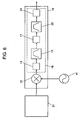
- Fig. 6 shows a conventional high-frequency module.
- mixing circuit 12 mixes a baseband signal fed from baseband section 31 with a local signal fed from oscillator 41.
- a spurious signal produced by mixing circuit 12 is attenuated by first filter 13 and second filter 22 of filter circuit 18.
- a desired high-frequency signal has thus been obtained.
- the spurious signal directly come from matching device 14 has an output level greater than that of the spurious signal given attenuation by first filter 13 and second filter 22, accordingly, the resultant spurious signal cannot maintain a desirable attenuation level.
- the output level of the spurious signal fed from the high-frequency module has undesirably increased.
- the present invention addresses the problem above. It is therefore the object to provide a high-frequency module capable of offering a spurious signal with a preferably suppressed output level.
- the structure of the present invention has the high-frequency circuit formed of two sections: the first high-frequency circuit having a first filter circuit, and the second high-frequency circuit having a second filter circuit.
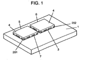
- Fig. 1 is a perspective view of high-frequency module 100 of an exemplary embodiment of the present invention.
- High-frequency module 100 of the present invention contains first high-frequency circuit 5 and second high-frequency circuit 6.
- first high-frequency circuit 5 of the present invention mixing circuit 12 and first filter circuit 16 are mounted on first circuit board 201, and over which, metallic case 4 is fixed to cover them.
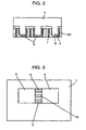
- Fig. 2 shows an enlarged side view of high-frequency module 100.
- Edge electrode 7 is formed at the side of first circuit board 201.
- high-frequency noise is shielded by electrically connecting between the GND electrode of edge electrode 7 and terminal 3 formed on metallic case 4 with solder 8.
- second high-frequency circuit 6 shown in Fig. 1 the second filter circuit is mounted on second circuit board 202.
- metallic case 4 covers components of the filter circuit.
- first high-frequency circuit 5 and second high-frequency circuit 6 are mounted on motherboard 1.
- the high-frequency circuit of the present invention is configured by establishing a high-frequency connection between the two circuits through signal line 10 on motherboard 1.
- the connecting line has an impedance of 50 ohm.
- GND pattern 9 is formed around the signal line to protect the signal line from an effect of noise, whereby the characteristics of the high-frequency module is maintained.
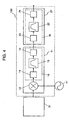
- Base band section 31 outputs a 380 MHz base band signal; on the other hand, oscillator 41 outputs a 1760 MHz local signal.
- the two signals are added at mixer 12 to be resultant output of 2140 MHz.
- the resultant signal passes through matching device 14 of first filter circuit 16 and enters into first filter 13.
- First filter 13 is a dielectric filter, which can substantially eliminate noise of a local signal, thereby attenuating the 1760 MHz spurious signal fed from mixer 12 by 50 dB to feed the signal to matching device 15.
- matching device 14 is located to the input side of first filter 13; on the other hand, matching device 15 is located to the output side of first filter 13. Such an arrangement decreases radiation caused by unmatched impedance.
- the spurious signal which is fed from the input side of matching device 14 and, without passing through first filter 13, fed into matching device 15, is attenuated more than 60 dB. That is, first filter circuit 16 can constantly keep 50 dB attenuation.
- covering first high-frequency circuit 11 with metallic case 4 can suppress the spurious signal fed from the circuit.
- Second filter 22 is a dielectric filter, which can substantially eliminate noise of a spurious signal, thereby attenuating the 1760 MHz spurious signal fed from mixer 12 by 50 dB to feed the signal to matching device 24.
- matching device 23 is located to the input side of second filter 22; on the other hand, matching device 24 is located to the output side of second filter 22. Such an arrangement decreases radiation caused by unmatched impedance.
- the spurious signal from the local signal which is fed from matching device 23 and, without passing through second filter 22, fed into matching device 24, is attenuated more than 60 dB.
- second filter circuit 19 can constantly keep 50 dB attenuation.
- first high-frequency circuit 11 and second high-frequency circuit 21 With the structure of first high-frequency circuit 11 and second high-frequency circuit 21, a desired amount of attenuation, i.e., 100 dB attenuation of the spurious signal can be achieved.
- high-frequency module 100 employs a matching device
- an amplifier and an isolator can be used with the matching device to obtain the similar effect.
- a structure employing dielectric filters for filter 13 and filter 22 it is not limited thereto; a high-frequency module employing filters with an excellent quality in eliminating noise, such as a surface acoustic wave (SAW) filter and a MEMS filter, can provide the similar effect.
- SAW surface acoustic wave
- a base band signal fed from base band section 31 has a frequency of 380 MHz, and a local signal has a frequency of 1760 MHz, it is not limited thereto; a structure in which a local signal has a frequency ranging from 1730 to 1790 MHz can provide the similar effect.
- a base band signal fed from base band section 31 has a frequency of 380 MHz, and a local signal has a frequency of 1760 MHz, it is not limited thereto; a structure in which a base band signal has a frequency ranging from 10 to 400 MHz can provide the similar effect.
- high-frequency circuit is covered with metallic case in order to suppress the spurious signal fed from the circuit.
- metallic case a conductive case formed of (a) an insulating resin for covering the circuits and (b) metal plating for covering a surface of the insulating resin can be also used.
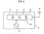
- Fig. 5 shows wireless device 61 employing high-frequency module 100 of the present invention.
- a base band signal fed from base band section 31 and a local signal fed from oscillator 41 are fed into first high-frequency circuit 11 to have frequency conversion.
- the signal from circuit 11 passes through second high-frequency circuit 21 and front-end section 62 and goes out from antenna 63 into the air.
- the wireless device employing high-frequency module 100 of the present invention is highly effective in attenuating a spurious signal, accordingly, the spurious signal radiated from antenna 63 is preferably suppressed.
- the wireless device capable of suppressing a spurious signal to a low level can thus be obtained.
- the high-frequency circuit is divided into two sections: a first high-frequency circuit having a first filter circuit, and a second high-frequency circuit having a second filter circuit.
- a high frequency module capable of suppressing the output of a spurious signal can be obtained.
Landscapes
- Transceivers (AREA)
- Transmitters (AREA)
- Control Of Motors That Do Not Use Commutators (AREA)
Claims (8)
- Hochfrequenzmodul (100) mit:a) einer ersten Hochfrequenzschaltung (11), die Folgendes aufweist:a-1) eine Mischschaltung (12) zum Mischen eines von einem Basisbandteil (31) eingespeisten Basisbandsignals mit einem von einem Oszillator (41) eingespeisten lokalen Signal unda-2) eine erste Filterschaltung (16) zum Abschwächen eines lokalen Verluststroms von der Mischschaltung (12); undb) einer zweiten Hochfrequenzschaltung (21) mit einer zweiten Filterschaltung (19) zum Abschwächen eines lokalen Verluststroms von der ersten Filterschaltung (16),wobei die erste Hochfrequenzschaltung (11) und/oder die zweite Hochfrequenzschaltung (21) mit einem gesonderten leitfähigen Gehäuse (4) ummantelt ist.
- Hochfrequenzmodul nach Anspruch 1, dadurch gekennzeichnet, dass das leitfähige Gehäuse aus Metall besteht.
- Hochfrequenzmodul nach Anspruch 1, dadurch gekennzeichnet, dass das leitfähige Gehäuse aus I) einem Isolierharz zum Ummanteln der Schaltungen und II) einem galvanischen Metallüberzug zum Bedecken einer Oberfläche des Isolierharzes besteht.
- Hochfrequenzmodul nach Anspruch 1, dadurch gekennzeichnet, dass die erste Filterschaltung und die zweite Filterschaltung ein dielektrisches Filter aufweisen.
- Hochfrequenzmodul nach Anspruch 1, dadurch gekennzeichnet, dass eine Signalleitung mit einer Impedanz von 50 Ω die erste Hochfrequenzschaltung mit der zweiten Hochfrequenzschaltung verbindet.
- Hochfrequenzmodul nach Anspruch 1, das weiterhin ein Motherboard aufweist, auf dem eine erste Leiterplatte, die die erste Hochfrequenzschaltung enthält, eine zweite Leiterplatte, die die zweite Hochfrequenzschaltung enthält, und die 50-Ω-Signalleitung montiert sind, die die erste Hochfrequenzschaltung mit der zweiten Hochfrequenzschaltung verbindet.
- Funkgerät, das ein Hochfrequenzmodul (100) verwendet, das Folgendes aufweist:a) eine erste Hochfrequenzschaltung (11), die weiterhin Folgendes aufweist:a-1) eine Mischschaltung (12) zum Mischen eines von einem Basisbandteil (31) eingespeisten Basisbandsignals mit einem von einem Oszillator (41) eingespeisten lokalen Signal unda-2) eine erste Filterschaltung (16) zum Abschwächen eines lokalen Verluststroms von der Mischschaltung (12); undb) eine zweite Hochfrequenzschaltung (21) mit einer zweiten Filterschaltung (19) zum Abschwächen eines lokalen Verluststroms von der ersten Filterschaltung (16),wobei die erste Hochfrequenzschaltung (11) und/oder die zweite Hochfrequenzschaltung (21) mit einem gesonderten leitfähigen Gehäuse (4) ummantelt ist.
- Funkgerät nach Anspruch 7, dadurch gekennzeichnet, dass das Hochfrequenzmodul ein Motherboard aufweist, auf dem eine erste Leiterplatte, die die erste Hochfrequenzschaltung enthält, eine zweite Leiterplatte, die die zweite Hochfrequenzschaltung enthält, und die 50-Ω-Signalleitung montiert sind, die die erste Hochfrequenzschaltung mit der zweiten Hochfrequenzschaltung verbindet.
Applications Claiming Priority (3)
| Application Number | Priority Date | Filing Date | Title |
|---|---|---|---|
| JP2002222788 | 2002-07-31 | ||
| JP2002222788A JP3988568B2 (ja) | 2002-07-31 | 2002-07-31 | 高周波モジュールおよびそれを用いた無線装置 |
| PCT/JP2003/009312 WO2004012351A1 (ja) | 2002-07-31 | 2003-07-23 | 高周波モジュールおよびそれを用いた無線装置 |
Publications (3)
| Publication Number | Publication Date |
|---|---|
| EP1429464A1 EP1429464A1 (de) | 2004-06-16 |
| EP1429464A4 EP1429464A4 (de) | 2004-10-27 |
| EP1429464B1 true EP1429464B1 (de) | 2009-06-24 |
Family
ID=31184930
Family Applications (1)
| Application Number | Title | Priority Date | Filing Date |
|---|---|---|---|
| EP03771286A Expired - Lifetime EP1429464B1 (de) | 2002-07-31 | 2003-07-23 | Hochfrequenzmodul und funkeinrichtung damit |
Country Status (6)
| Country | Link |
|---|---|
| US (1) | US7120409B2 (de) |
| EP (1) | EP1429464B1 (de) |
| JP (1) | JP3988568B2 (de) |
| CN (1) | CN100352169C (de) |
| DE (1) | DE60328075D1 (de) |
| WO (1) | WO2004012351A1 (de) |
Families Citing this family (2)
| Publication number | Priority date | Publication date | Assignee | Title |
|---|---|---|---|---|
| EP3764703B1 (de) * | 2014-09-28 | 2024-02-28 | Huawei Technologies Co., Ltd. | Verfahren und vorrichtung zur steuerung der uplink-leistung |
| JP2016163119A (ja) * | 2015-02-27 | 2016-09-05 | 三菱電機株式会社 | フェーズドアレーアンテナ装置及びフェーズドアレーアンテナの制御方法 |
Family Cites Families (20)
| Publication number | Priority date | Publication date | Assignee | Title |
|---|---|---|---|---|
| JPS57200944A (en) | 1981-06-02 | 1982-12-09 | Hitachi Ltd | Manufacture of magnetic disk |
| JPS6216033Y2 (de) * | 1981-06-15 | 1987-04-23 | ||
| JPS58204627A (ja) * | 1982-05-21 | 1983-11-29 | Toshiba Corp | チユ−ナ装置 |
| US4661998A (en) * | 1983-09-22 | 1987-04-28 | Matsushita Electric Industrial Co. Ltd. | Double superheterodyne tuner |
| JP3114183B2 (ja) * | 1990-04-19 | 2000-12-04 | 日本電気株式会社 | 受信機 |
| JPH09270828A (ja) | 1996-04-01 | 1997-10-14 | Toshiba Corp | 無線送信機 |
| US5764492A (en) * | 1996-07-08 | 1998-06-09 | Motorola, Inc. | Radio device with radio shielding and method of manufacture |
| JP3087664B2 (ja) * | 1996-11-06 | 2000-09-11 | 株式会社村田製作所 | 誘電体共振器装置及び高周波モジュール |
| JPH10285060A (ja) | 1997-04-02 | 1998-10-23 | Kokusai Electric Co Ltd | 無線送信機 |
| JPH11214927A (ja) * | 1998-01-29 | 1999-08-06 | Murata Mfg Co Ltd | 高周波モジュール |
| JP3406830B2 (ja) * | 1998-03-06 | 2003-05-19 | 京セラ株式会社 | 高周波用電子装置 |
| JP2001218120A (ja) | 2000-01-02 | 2001-08-10 | Alps Electric Co Ltd | ケーブルテレビジョン送信機の周波数変換回路 |
| JP2002043805A (ja) | 2000-07-28 | 2002-02-08 | Tamagawa Electronics Co Ltd | バンドパスフィルタ |
| JP2002359290A (ja) * | 2001-03-27 | 2002-12-13 | Matsushita Electric Ind Co Ltd | 半導体集積装置 |
| JP3612031B2 (ja) * | 2001-03-29 | 2005-01-19 | Tdk株式会社 | 高周波モジュール |
| JP3973402B2 (ja) * | 2001-10-25 | 2007-09-12 | 株式会社日立製作所 | 高周波回路モジュール |
| US6815796B2 (en) * | 2001-12-07 | 2004-11-09 | Taiyo Yuden Co., Ltd. | Composite module and process of producing same |
| JP3786031B2 (ja) * | 2002-02-26 | 2006-06-14 | 株式会社村田製作所 | 高周波回路装置および送受信装置 |
| US7155195B2 (en) * | 2002-06-14 | 2006-12-26 | Skyworks Solutions, Inc. | Input and output filtering system for a direct conversion receiver |
| JP2004032184A (ja) * | 2002-06-24 | 2004-01-29 | Murata Mfg Co Ltd | 高周波モジュール、送受信装置および高周波モジュールの特性調整方法 |
-
2002
- 2002-07-31 JP JP2002222788A patent/JP3988568B2/ja not_active Expired - Fee Related
-
2003
- 2003-07-23 EP EP03771286A patent/EP1429464B1/de not_active Expired - Lifetime
- 2003-07-23 CN CNB038011352A patent/CN100352169C/zh not_active Expired - Fee Related
- 2003-07-23 DE DE60328075T patent/DE60328075D1/de not_active Expired - Lifetime
- 2003-07-23 US US10/491,127 patent/US7120409B2/en not_active Expired - Fee Related
- 2003-07-23 WO PCT/JP2003/009312 patent/WO2004012351A1/ja not_active Ceased
Also Published As
| Publication number | Publication date |
|---|---|
| WO2004012351A1 (ja) | 2004-02-05 |
| JP3988568B2 (ja) | 2007-10-10 |
| US20050003779A1 (en) | 2005-01-06 |
| EP1429464A4 (de) | 2004-10-27 |
| DE60328075D1 (de) | 2009-08-06 |
| CN1565084A (zh) | 2005-01-12 |
| JP2004064609A (ja) | 2004-02-26 |
| US7120409B2 (en) | 2006-10-10 |
| CN100352169C (zh) | 2007-11-28 |
| EP1429464A1 (de) | 2004-06-16 |
Similar Documents
| Publication | Publication Date | Title |
|---|---|---|
| US6961544B1 (en) | Structure of a radio-frequency front end | |
| US7053731B2 (en) | Duplexer using surface acoustic wave filters | |
| JP5123292B2 (ja) | 電気的素子 | |
| US7941103B2 (en) | Duplexer | |
| US7733196B2 (en) | Antenna sharing device | |
| JP5583977B2 (ja) | フィルタ、分波器、通信モジュール、および通信装置 | |
| US6996384B2 (en) | Receiver and radio communication terminal using the same | |
| US20220190868A1 (en) | Wireless communication module | |
| US7046982B2 (en) | High frequency device having a frame with segmented compartments for prevented unwanted signal propagation | |
| US20140312978A1 (en) | High-frequency module | |
| US7120409B2 (en) | High frequency module and radio device using the same | |
| US20250175143A1 (en) | Acoustic wave device, high frequency module, and communication device | |
| TW200845605A (en) | Sending/receiving circuit module | |
| US8014161B2 (en) | Communication device and electronic apparatus using the same | |
| US7194245B2 (en) | High-frequency signal receiving apparatus | |
| JP3576465B2 (ja) | 高周波半導体装置およびそれを用いた携帯用通信機器 | |
| JPH07297670A (ja) | 高周波回路基板 | |
| EP0828306A2 (de) | Filter mit angepassten Impedanzen | |
| JPH04233310A (ja) | バンドパスフィルタ回路 | |
| KR20040011726A (ko) | 안테나 스위치 모듈 측정장치 및 그 제조방법 | |
| KR20070080936A (ko) | 수신감도를 향상시키기 위한 차폐 구조의 프런트 엔드 모듈 | |
| JPH0650823B2 (ja) | 高周波信号接続装置 | |
| JPH0742232U (ja) | 無線通信機用送受信装置 | |
| JPH0742191U (ja) | 無線通信機用送受信装置 | |
| JPH0742230U (ja) | 無線通信機用送受信装置 |
Legal Events
| Date | Code | Title | Description |
|---|---|---|---|
| PUAI | Public reference made under article 153(3) epc to a published international application that has entered the european phase |
Free format text: ORIGINAL CODE: 0009012 |
|
| 17P | Request for examination filed |
Effective date: 20040326 |
|
| AK | Designated contracting states |
Kind code of ref document: A1 Designated state(s): AT BE BG CH CY CZ DE DK EE ES FI FR GB GR HU IE IT LI LU MC NL PT RO SE SI SK TR |
|
| AX | Request for extension of the european patent |
Extension state: AL LT LV MK |
|
| A4 | Supplementary search report drawn up and despatched |
Effective date: 20040913 |
|
| RIC1 | Information provided on ipc code assigned before grant |
Ipc: 7H 04B 1/03 A Ipc: 7H 01P 1/20 B |
|
| DAX | Request for extension of the european patent (deleted) | ||
| RBV | Designated contracting states (corrected) |
Designated state(s): DE FR GB |
|
| GRAP | Despatch of communication of intention to grant a patent |
Free format text: ORIGINAL CODE: EPIDOSNIGR1 |
|
| RAP1 | Party data changed (applicant data changed or rights of an application transferred) |
Owner name: MATSUSHITA ELECTRIC INDUSTRIAL CO., LTD. |
|
| RAP1 | Party data changed (applicant data changed or rights of an application transferred) |
Owner name: PANASONIC CORPORATION |
|
| GRAS | Grant fee paid |
Free format text: ORIGINAL CODE: EPIDOSNIGR3 |
|
| GRAA | (expected) grant |
Free format text: ORIGINAL CODE: 0009210 |
|
| AK | Designated contracting states |
Kind code of ref document: B1 Designated state(s): DE FR GB |
|
| REG | Reference to a national code |
Ref country code: GB Ref legal event code: FG4D |
|
| REF | Corresponds to: |
Ref document number: 60328075 Country of ref document: DE Date of ref document: 20090806 Kind code of ref document: P |
|
| PLBE | No opposition filed within time limit |
Free format text: ORIGINAL CODE: 0009261 |
|
| STAA | Information on the status of an ep patent application or granted ep patent |
Free format text: STATUS: NO OPPOSITION FILED WITHIN TIME LIMIT |
|
| 26N | No opposition filed |
Effective date: 20100325 |
|
| REG | Reference to a national code |
Ref country code: DE Ref legal event code: R084 Ref document number: 60328075 Country of ref document: DE Effective date: 20111010 |
|
| PGFP | Annual fee paid to national office [announced via postgrant information from national office to epo] |
Ref country code: DE Payment date: 20140716 Year of fee payment: 12 |
|
| PGFP | Annual fee paid to national office [announced via postgrant information from national office to epo] |
Ref country code: GB Payment date: 20140723 Year of fee payment: 12 Ref country code: FR Payment date: 20140708 Year of fee payment: 12 |
|
| REG | Reference to a national code |
Ref country code: DE Ref legal event code: R119 Ref document number: 60328075 Country of ref document: DE |
|
| GBPC | Gb: european patent ceased through non-payment of renewal fee |
Effective date: 20150723 |
|
| PG25 | Lapsed in a contracting state [announced via postgrant information from national office to epo] |
Ref country code: GB Free format text: LAPSE BECAUSE OF NON-PAYMENT OF DUE FEES Effective date: 20150723 Ref country code: DE Free format text: LAPSE BECAUSE OF NON-PAYMENT OF DUE FEES Effective date: 20160202 |
|
| REG | Reference to a national code |
Ref country code: FR Ref legal event code: ST Effective date: 20160331 |
|
| PG25 | Lapsed in a contracting state [announced via postgrant information from national office to epo] |
Ref country code: FR Free format text: LAPSE BECAUSE OF NON-PAYMENT OF DUE FEES Effective date: 20150731 |