EP1429311A2 - Anzeigesteuerungsvorrichtung, Anzeigesystem und Anzeigesteuerungsverfahrung - Google Patents
Anzeigesteuerungsvorrichtung, Anzeigesystem und Anzeigesteuerungsverfahrung Download PDFInfo
- Publication number
- EP1429311A2 EP1429311A2 EP03257271A EP03257271A EP1429311A2 EP 1429311 A2 EP1429311 A2 EP 1429311A2 EP 03257271 A EP03257271 A EP 03257271A EP 03257271 A EP03257271 A EP 03257271A EP 1429311 A2 EP1429311 A2 EP 1429311A2
- Authority
- EP
- European Patent Office
- Prior art keywords
- scanning
- display
- line
- pixel
- driving
- Prior art date
- Legal status (The legal status is an assumption and is not a legal conclusion. Google has not performed a legal analysis and makes no representation as to the accuracy of the status listed.)
- Withdrawn
Links
Images


Classifications
-
- G—PHYSICS
- G09—EDUCATION; CRYPTOGRAPHY; DISPLAY; ADVERTISING; SEALS
- G09G—ARRANGEMENTS OR CIRCUITS FOR CONTROL OF INDICATING DEVICES USING STATIC MEANS TO PRESENT VARIABLE INFORMATION
- G09G3/00—Control arrangements or circuits, of interest only in connection with visual indicators other than cathode-ray tubes
- G09G3/20—Control arrangements or circuits, of interest only in connection with visual indicators other than cathode-ray tubes for presentation of an assembly of a number of characters, e.g. a page, by composing the assembly by combination of individual elements arranged in a matrix no fixed position being assigned to or needed to be assigned to the individual characters or partial characters
- G09G3/22—Control arrangements or circuits, of interest only in connection with visual indicators other than cathode-ray tubes for presentation of an assembly of a number of characters, e.g. a page, by composing the assembly by combination of individual elements arranged in a matrix no fixed position being assigned to or needed to be assigned to the individual characters or partial characters using controlled light sources
- G09G3/30—Control arrangements or circuits, of interest only in connection with visual indicators other than cathode-ray tubes for presentation of an assembly of a number of characters, e.g. a page, by composing the assembly by combination of individual elements arranged in a matrix no fixed position being assigned to or needed to be assigned to the individual characters or partial characters using controlled light sources using electroluminescent panels
- G09G3/32—Control arrangements or circuits, of interest only in connection with visual indicators other than cathode-ray tubes for presentation of an assembly of a number of characters, e.g. a page, by composing the assembly by combination of individual elements arranged in a matrix no fixed position being assigned to or needed to be assigned to the individual characters or partial characters using controlled light sources using electroluminescent panels semiconductive, e.g. using light-emitting diodes [LED]
- G09G3/3208—Control arrangements or circuits, of interest only in connection with visual indicators other than cathode-ray tubes for presentation of an assembly of a number of characters, e.g. a page, by composing the assembly by combination of individual elements arranged in a matrix no fixed position being assigned to or needed to be assigned to the individual characters or partial characters using controlled light sources using electroluminescent panels semiconductive, e.g. using light-emitting diodes [LED] organic, e.g. using organic light-emitting diodes [OLED]
- G09G3/3225—Control arrangements or circuits, of interest only in connection with visual indicators other than cathode-ray tubes for presentation of an assembly of a number of characters, e.g. a page, by composing the assembly by combination of individual elements arranged in a matrix no fixed position being assigned to or needed to be assigned to the individual characters or partial characters using controlled light sources using electroluminescent panels semiconductive, e.g. using light-emitting diodes [LED] organic, e.g. using organic light-emitting diodes [OLED] using an active matrix
-
- G—PHYSICS
- G09—EDUCATION; CRYPTOGRAPHY; DISPLAY; ADVERTISING; SEALS
- G09G—ARRANGEMENTS OR CIRCUITS FOR CONTROL OF INDICATING DEVICES USING STATIC MEANS TO PRESENT VARIABLE INFORMATION
- G09G2300/00—Aspects of the constitution of display devices
- G09G2300/08—Active matrix structure, i.e. with use of active elements, inclusive of non-linear two terminal elements, in the pixels together with light emitting or modulating elements
-
- G—PHYSICS
- G09—EDUCATION; CRYPTOGRAPHY; DISPLAY; ADVERTISING; SEALS
- G09G—ARRANGEMENTS OR CIRCUITS FOR CONTROL OF INDICATING DEVICES USING STATIC MEANS TO PRESENT VARIABLE INFORMATION
- G09G2300/00—Aspects of the constitution of display devices
- G09G2300/08—Active matrix structure, i.e. with use of active elements, inclusive of non-linear two terminal elements, in the pixels together with light emitting or modulating elements
- G09G2300/0809—Several active elements per pixel in active matrix panels
- G09G2300/0842—Several active elements per pixel in active matrix panels forming a memory circuit, e.g. a dynamic memory with one capacitor
-
- G—PHYSICS
- G09—EDUCATION; CRYPTOGRAPHY; DISPLAY; ADVERTISING; SEALS
- G09G—ARRANGEMENTS OR CIRCUITS FOR CONTROL OF INDICATING DEVICES USING STATIC MEANS TO PRESENT VARIABLE INFORMATION
- G09G2300/00—Aspects of the constitution of display devices
- G09G2300/08—Active matrix structure, i.e. with use of active elements, inclusive of non-linear two terminal elements, in the pixels together with light emitting or modulating elements
- G09G2300/0809—Several active elements per pixel in active matrix panels
- G09G2300/0842—Several active elements per pixel in active matrix panels forming a memory circuit, e.g. a dynamic memory with one capacitor
- G09G2300/0861—Several active elements per pixel in active matrix panels forming a memory circuit, e.g. a dynamic memory with one capacitor with additional control of the display period without amending the charge stored in a pixel memory, e.g. by means of additional select electrodes
-
- G—PHYSICS
- G09—EDUCATION; CRYPTOGRAPHY; DISPLAY; ADVERTISING; SEALS
- G09G—ARRANGEMENTS OR CIRCUITS FOR CONTROL OF INDICATING DEVICES USING STATIC MEANS TO PRESENT VARIABLE INFORMATION
- G09G2300/00—Aspects of the constitution of display devices
- G09G2300/08—Active matrix structure, i.e. with use of active elements, inclusive of non-linear two terminal elements, in the pixels together with light emitting or modulating elements
- G09G2300/0809—Several active elements per pixel in active matrix panels
- G09G2300/0842—Several active elements per pixel in active matrix panels forming a memory circuit, e.g. a dynamic memory with one capacitor
- G09G2300/0861—Several active elements per pixel in active matrix panels forming a memory circuit, e.g. a dynamic memory with one capacitor with additional control of the display period without amending the charge stored in a pixel memory, e.g. by means of additional select electrodes
- G09G2300/0866—Several active elements per pixel in active matrix panels forming a memory circuit, e.g. a dynamic memory with one capacitor with additional control of the display period without amending the charge stored in a pixel memory, e.g. by means of additional select electrodes by means of changes in the pixel supply voltage
-
- G—PHYSICS
- G09—EDUCATION; CRYPTOGRAPHY; DISPLAY; ADVERTISING; SEALS
- G09G—ARRANGEMENTS OR CIRCUITS FOR CONTROL OF INDICATING DEVICES USING STATIC MEANS TO PRESENT VARIABLE INFORMATION
- G09G2310/00—Command of the display device
- G09G2310/02—Addressing, scanning or driving the display screen or processing steps related thereto
- G09G2310/0202—Addressing of scan or signal lines
- G09G2310/0213—Addressing of scan or signal lines controlling the sequence of the scanning lines with respect to the patterns to be displayed, e.g. to save power
-
- G—PHYSICS
- G09—EDUCATION; CRYPTOGRAPHY; DISPLAY; ADVERTISING; SEALS
- G09G—ARRANGEMENTS OR CIRCUITS FOR CONTROL OF INDICATING DEVICES USING STATIC MEANS TO PRESENT VARIABLE INFORMATION
- G09G2310/00—Command of the display device
- G09G2310/02—Addressing, scanning or driving the display screen or processing steps related thereto
- G09G2310/0202—Addressing of scan or signal lines
- G09G2310/0218—Addressing of scan or signal lines with collection of electrodes in groups for n-dimensional addressing
-
- G—PHYSICS
- G09—EDUCATION; CRYPTOGRAPHY; DISPLAY; ADVERTISING; SEALS
- G09G—ARRANGEMENTS OR CIRCUITS FOR CONTROL OF INDICATING DEVICES USING STATIC MEANS TO PRESENT VARIABLE INFORMATION
- G09G2320/00—Control of display operating conditions
- G09G2320/02—Improving the quality of display appearance
- G09G2320/0257—Reduction of after-image effects
-
- G—PHYSICS
- G09—EDUCATION; CRYPTOGRAPHY; DISPLAY; ADVERTISING; SEALS
- G09G—ARRANGEMENTS OR CIRCUITS FOR CONTROL OF INDICATING DEVICES USING STATIC MEANS TO PRESENT VARIABLE INFORMATION
- G09G2320/00—Control of display operating conditions
- G09G2320/02—Improving the quality of display appearance
- G09G2320/0261—Improving the quality of display appearance in the context of movement of objects on the screen or movement of the observer relative to the screen
-
- G—PHYSICS
- G09—EDUCATION; CRYPTOGRAPHY; DISPLAY; ADVERTISING; SEALS
- G09G—ARRANGEMENTS OR CIRCUITS FOR CONTROL OF INDICATING DEVICES USING STATIC MEANS TO PRESENT VARIABLE INFORMATION
- G09G2330/00—Aspects of power supply; Aspects of display protection and defect management
- G09G2330/02—Details of power systems and of start or stop of display operation
- G09G2330/021—Power management, e.g. power saving
-
- G—PHYSICS
- G09—EDUCATION; CRYPTOGRAPHY; DISPLAY; ADVERTISING; SEALS
- G09G—ARRANGEMENTS OR CIRCUITS FOR CONTROL OF INDICATING DEVICES USING STATIC MEANS TO PRESENT VARIABLE INFORMATION
- G09G3/00—Control arrangements or circuits, of interest only in connection with visual indicators other than cathode-ray tubes
- G09G3/20—Control arrangements or circuits, of interest only in connection with visual indicators other than cathode-ray tubes for presentation of an assembly of a number of characters, e.g. a page, by composing the assembly by combination of individual elements arranged in a matrix no fixed position being assigned to or needed to be assigned to the individual characters or partial characters
-
- G—PHYSICS
- G09—EDUCATION; CRYPTOGRAPHY; DISPLAY; ADVERTISING; SEALS
- G09G—ARRANGEMENTS OR CIRCUITS FOR CONTROL OF INDICATING DEVICES USING STATIC MEANS TO PRESENT VARIABLE INFORMATION
- G09G3/00—Control arrangements or circuits, of interest only in connection with visual indicators other than cathode-ray tubes
- G09G3/20—Control arrangements or circuits, of interest only in connection with visual indicators other than cathode-ray tubes for presentation of an assembly of a number of characters, e.g. a page, by composing the assembly by combination of individual elements arranged in a matrix no fixed position being assigned to or needed to be assigned to the individual characters or partial characters
- G09G3/2007—Display of intermediate tones
- G09G3/2018—Display of intermediate tones by time modulation using two or more time intervals
- G09G3/2022—Display of intermediate tones by time modulation using two or more time intervals using sub-frames
Definitions
- the present invention relates to a technical field of a display controller, a display system, and a display controlling method.
- the present invention relates to a technical field of a display controller for controlling a display pattern in a matrix display apparatus, a display system including the display controller and the display apparatus, and a display controlling method performed in the display controller.
- the following display method is generally adopted: in a vertical synchronizing period from when voltage information is supplied to each pixel constituting a display screen to when the subsequent voltage information is supplied, the supplied voltage information is stored by using a pixel capacity formed in each pixel, so that light emission from the pixel is continued.
- the supplied voltage information is stored using a pixel capacity during one vertical synchronizing period all, so that light emission from the pixel is continued.
- an afterimage resulting from human vision is more likely to occur.
- Such an afterimage reduces display quality. For example, a fast moving image cannot be clearly displayed.
- An object of the present invention is to provide a display controller for controlling the display of a fast moving image with higher quality in a active matrix display apparatus constituted of a plurality of pixels, each including an active element, to provide a display system including the display controller and the display apparatus, and to provide a display controlling method performed in the display controller.
- the above object of the present invention can be achieved by a display controller for controlling a display pattern of an image in a display apparatus constituted of a plurality of pixels arranged in a matrix form, the each pixel including a pixel-driving device.
- the display controller is provided with a driving control device for controlling an operation of the pixel-driving devices, based on image information corresponding to the image to be displayed during a synchronizing period of one synchronizing direction, only for predetermined illuminating period shorter than the synchronizing period.
- the pixel-driving devices in the pixels are driven to display an image only in the illuminating period shorter than one vertical synchronizing period.
- the driving control device simultaneously drives all the pixel-driving devices based on the image information only during the illuminating period.
- the driving control device drives, based on the image information, the pixel-driving devices which are on one scanning line during the synchronizing period so as to line-sequentially perform scanning.
- the pixel-driving devices which are on one scanning line during the synchronizing period so as to line-sequentially perform scanning, it is possible to reduce the influence of an afterimage in human vision and control the display of a fast moving image with higher quality.
- the driving control device drives the pixel-driving devices on the adjacent two or more scanning lines included in a scanning-line-group simultaneously, and drives the pixel-driving devices in the scanning-line-group in a direction perpendicular to the scanning direction of the scanning line while displacing the scanning line one after another.
- the pixel-driving devices on the adjacent two or more scanning lines included in the scanning-line-group are driven simultaneously and the pixel-driving devices in the scanning-line-group are driven in a direction perpendicular to the scanning direction of the scanning line while displacing the scanning line one after another, it is possible to reduce the influence of an afterimage in human vision and control the display of a fast moving image with higher quality.
- the driving control device drives the pixel-driving devices on the scanning lines, for each of a plurality of scanning-line-groups each being constituted of the adjacent two or more scanning lines and including a different number of the scanning lines, drives the pixel-driving devices in the scanning-line-group simultaneously, and drives the pixel-driving devices in the scanning-line-group in a direction perpendicular to the scanning direction of the scanning line while displacing the scanning line one after another.
- the pixel-driving devices on the adjacent two or more scanning lines included in the scanning-line-group are driven simultaneously, for each of a plurality of scanning-line-groups each being constituted of the adjacent two or more scanning lines and including a different number of the scanning lines, and are driven in a direction perpendicular to the scanning direction of the scanning line while displacing the scanning line one after another, it is possible to perform control to clearly display the moving image even when gray scale display is provided for the moving image.
- the display control device drives the pixel-driving devices in each scanning-line-group during the synchronizing, and the number of the scanning lines of each scanning-line-group is simply increased or simply reduced along the synchronizing direction.
- the synchronizing period in the image information is constituted of a plurality of sub synchronizing periods each having a different weight of an image display period
- the driving control device performs selection writing scanning for line-sequentially scanning the pixel-driving device on the scanning line corresponding to the sub synchronizing period based on the image information and placing the pixel on the scanning line into an image display state in each of the sub synchronizing periods
- the driving control device performs non-display scanning for line-sequentially scanning the pixel-driving devices on the scanning line to be subjected to the selection writing scanning and placing all the pixels on the scanning line into an image non-display state before starting the selection writing scanning on the scanning line.
- selection writing scanning is performed in each of the sub synchronizing periods to place the pixels on the corresponding scanning lines into an image display state based on moving image information and a non-display scanning is performed to place into an image non-display state all of the pixels on the scanning lines to be subjected to the selection writing scanning before the selection writing scanning is started on the scanning lines, it is possible to reduce the occurrence of a moving image false contour when gray scale display is provided by the sub synchronizing period method.
- the above object of the present invention can be achieved by a display system.
- the display system is provided with: a display controller for controlling a display pattern of an image in a display apparatus constituted of a plurality of pixels arranged in a matrix form, the each pixel including a pixel-driving device, the display controller comprising a driving control device for controlling an operation of the pixel-driving devices, based on image information corresponding to the image to be displayed during a synchronizing period of one synchronizing direction, only for predetermined illuminating period shorter than the synchronizing period, and the display apparatus.
- the pixel-driving devices in the pixels are driven to display an image only in the illuminating period shorter than one vertical synchronizing period.
- the above object of the present invention can be achieved by a display controlling method for controlling a display pattern of an image in a display apparatus constituted of a plurality of pixels arranged in a matrix form, the pixel including a pixel-driving device.
- the display controlling method is provided with a driving controlling process for controlling an operation of the pixel-driving device, based on image information corresponding to the image to be displayed during a synchronizing period of one synchronizing direction, only for predetermined illuminating period shorter than the synchronizing period.
- the pixel-driving devices in the pixels are driven to display an image only in the illuminating period shorter than one vertical synchronizing period.
- the active matrix display has a driving element such as a thin film transistor (TFT) in each pixel to display a moving image and so on.
- TFT thin film transistor
- Embodiment 1 of the present invention will be firstly described.
- FIG. 1 is a block diagram showing the schematic configuration of a display apparatus according to Embodiment 1.
- FIG. 2 is a circuit diagram showing the configuration of elements in each pixel included in a display part of the display apparatus.
- FIG. 3 is a timing chart showing a driving state of the display apparatus.
- a display apparatus SS of Embodiment 1 is constituted of a display controller 1 serving as a driving control device including a frame memory 1A, a data driver 2, a gate driver 3, a display part DD, a direct-current voltage power supply V for generating direct-current voltage of a constant voltage, and a switch SW.
- a display controller 1 serving as a driving control device including a frame memory 1A, a data driver 2, a gate driver 3, a display part DD, a direct-current voltage power supply V for generating direct-current voltage of a constant voltage, and a switch SW.
- the display part DD is constituted of a plurality of pixels S arranged in a matrix form of n rows and m columns.
- the pixels S are numbered according to the rows and columns of the display part DD.
- the data driver 2 and the pixels S are connected via data lines D 1 to D m .
- the gate driver 3 and the pixels S are connected via gate lines G 1 to G n .
- the positive pole of the direct-current voltage power supply V is connected to the pixels S via the switch SW having been turned on and an anode line A. Meanwhile, the negative pole of the direct-current voltage power supply V is connected to the pixels S via a cathode line K.
- the switch SW turns on/off the connection between the positive pole of the direct-current voltage power supply V and the anode line A in response to a switching signal outputted from the display controller 1 via a control line Ssw, which is connected to the display controller 1.
- the data driver 2 outputs a data signal, which is provided for realizing a control pattern described later, via the data lines D 1 to D m to the pixels S in response to a driving signal outputted from the display controller 1 via a control line Sdd, which is connected to the display controller 1.
- the gate driver 3 outputs a gate signal, which is provided for realizing a control pattern described later, via the gate lines G 1 to G n to the pixels S in response to a driving signal outputted from the display controller 1 via a control line Sdg, which is connected to the display controller 1.
- the display controller 1 controls the switching of the switch SW, generates the switching signal for realizing a display pattern of Embodiment 1, and outputs the signal via the control line Ssw to the switch SW.
- the pixel S in the display part DD is constituted of transistors T and TT serving as a pixel-driving device and an active element, a capacitor C, and a light-emitting device E such as an organic EL light-emitting device.
- the gate terminal of the transistor T is connected to the gate line G which corresponds to the pixel S
- the source terminal of the transistor T is connected to the data line D which corresponds to the pixel S
- the drain terminal of the transistor T is connected to the gate terminal of the transistor TT, which is another transistor in the same pixel, and is connected to one terminal of the capacitor C in the same pixel S.
- the other terminal of the capacitor C is grounded.
- the source terminal of the transistor TT is connected to the anode line A, and the drain terminal of the transistor TT is connected to one terminal of the light-emitting device E.
- the other terminal of the light-emitting device E is connected to the corresponding cathode line K.
- the transistor T when the data signal is supplied via the data line D while the pixel S including the transistor T is selected according to the gate signal supplied via the gate line G, the transistor T is turned on by the selection according to the gate signal.
- the data signal is supplied to the capacitor C so as to charge the capacitor C.
- the gate terminal of the transistor TT increases in potential with charging voltage, the transistor TT is turned on.
- scanning lines connected to one of the gate lines G that is scanning lines constituted of pixels arranged along the row direction of FIG. 1 are represented as L1, L2, L3, ..., L n .
- the gate signal in an address period starting from the beginning of one vertical synchronizing period, firstly based on moving image information (specifically indicates luminance information for each of the pixels S to be illuminated, also in the following description) transmitted via the information line Sdp, the gate signal permits the selection of a scanning line L which includes the pixels S having the light-emitting devices E to be illuminated in the vertical synchronizing period including the address period. Subsequently, among the pixels S arranged on the selected scanning line L, the data signal is supplied to the pixels S including the light-emitting devices E to be actually illuminated and the capacitors C are charged.
- moving image information specifically indicates luminance information for each of the pixels S to be illuminated, also in the following description
- a switching signal for turning off the switch SW is generated and is outputted to the switch SW.
- the gate signal of the transistor TT is also increased in voltage.
- the transistor TT is turned on. According to the circuit configuration of FIG. 2, even when only the transistor TT is turned on, the light-emitting element E is not illuminated unless current voltage from the direct-current voltage power supply V is applied between the anode line A and the cathode K.
- the direct-current voltage is applied between the anode terminal and the cathode terminal of the light-emitting device E, via the transistor TT having been turned on, by the switching operation.
- Current generated by the application of the direct-current voltage continues the illuminating operation of the light-emitting device E during the illuminating period.
- the illuminating operation is performed on the light-emitting devices E in all of the selected pixels S and is continued until the end of the vertical synchronizing period as shown in FIG. 3 (indicated as "illuminating state" in FIG. 3). In this case, the switch SW remains turned on during the illuminating period.
- the light-emitting luminance of the illuminating operation is a luminance corresponding to luminance information serving as the moving image information.
- the switching signal is outputted to turn off the switch SW after a lapse of one vertical synchronizing period during the illuminating operation, so that the illuminating operation is stopped and another vertical synchronizing period (address period) is started.
- the selection of the pixels S, the charging of the capacitors C, the standby until the start of the illuminating period, and the illuminating operation performed only in the illuminating period are repeated in all the vertical synchronizing periods, so that the illuminating operation is performed only in the illuminating period of the vertical synchronizing period.
- the light-emitting devices E in the pixels S are driven to display an image only in the illuminating period shorter than the vertical synchronizing period.
- the influence of an afterimage in human vision it is possible to reduce the influence of an afterimage in human vision and control the display of a fast moving image with higher quality.
- Embodiment 2 which is another embodiment of the present application.
- FIG. 4 is a block diagram showing the schematic configuration of a display apparatus according to Embodiment 2.
- FIG. 5 is a timing chart showing a driving state of the display apparatus in a vertical synchronizing period.
- FIG. 6 is a timing chart showing driving states in a plurality of vertical synchronizing periods of the display apparatus.
- FIG. 4 the same components as the display apparatus SS of Embodiment 1 shown in FIGs. 1 and 2 are indicated by the same reference numerals and the detailed explanation thereof is omitted.
- Embodiment 1 The above-described display apparatus SS of Embodiment 1 is configured so that all the light-emitting devices E are simultaneously illuminated only during the predetermined illuminating period in the vertical synchronizing period.
- Embodiment 2 an image is displayed by simultaneously driving light-emitting devices E on a plurality of adjacent scanning lines L, and is displayed by driving light-emitting devices E on a plurality of adjacent scanning lines L in a direction perpendicular to the scanning direction of the scanning line L while displacing the scanning line L one after another.
- a display apparatus SS1 of Embodiment 2 is constituted of a direct-current voltage power supply V and a display controller 10 including a frame memory 10A in addition to the data driver 2, the gate driver 3, and the display part DD in the display apparatus SS of Embodiment 1.
- the direct-current voltage power supply V is directly connected to an anode line A and a cathode line K which are connected to pixels S.
- the positive pole of the direct-current voltage power supply V is directly connected to the anode line A and the negative pole thereof is directly connected to the cathode line K.
- the display controller 10 is connected to the data driver 2 and the gate driver 3 via control lines Sdd and Sdg. Moving image information to be displayed on a display part DD is transmitted from the outside via an information line Sdp.
- scanning lines which are constituted of pixels S connected to one gate line G are represented as L1, L2, L3, ..., L n in FIGs. 5 and 6.
- a gate signal permits the selection of the scanning lines L which include the pixels S having the light-emitting devices E to be illuminated in the vertical synchronizing period. Subsequently, among the pixels S arranged on the selected scanning lines L, a data signal is supplied line-sequentially to the pixels S including the light-emitting devices E to be actually illuminated, so that capacitors C are charged. In this case, direct-current voltage generated by the direct-current voltage power supply V is always applied between the anode line A and the cathode line K during the vertical synchronizing period.
- the capacitor C of FIG. 2 is increased in charging voltage by the selection and charging performed by the data signal.
- the direct-current voltage is applied between the anode terminal and the cathode terminal of the light-emitting device E via the transistor TT having been turned on. Current generated by the application of the direct-current voltage line-sequentially starts illuminating the light-emitting devices E.
- FIG. 5 a change (displacement) in the timing of starting the illuminating operation on each of the scanning lines L is indicated by broken lines "A1".
- the illuminating operation is started immediately after the pixels S to be illuminated are selected line-sequentially and the charging of the corresponding capacitors C is completed.
- the illuminating operation is continued for equal illuminating period on each of the scanning lines L until an extinguishing operation is performed.
- the gate signal permits the selection of the scanning lines L which include the pixels S having the light-emitting devices E to be extinguished. Subsequently, among the pixels S arranged on the selected scanning lines L, an extinguishing signal (not shown) is supplied line-sequentially to the pixels S including the light-emitting devices E to be extinguished, so that the illuminating operation on the light-emitting devices E is stopped. Thus, the extinguishing operation is line-sequentially performed on the light-emitting devices E.
- a broken line "B2" indicates a change (displacement) in the timing of starting the extinguishing operation on each of the scanning lines L after the illuminating operation is started on the light-emitting devices E for each of the scanning lines L at the timing of the broken lines A1.
- the extinguishing operation is line-sequentially started on each of the illuminated pixels S for each of the scanning lines L.
- the extinguishment is continued until another illuminating operation is started on each of the scanning lines L in the subsequent vertical synchronizing period.
- broken lines "B 1" indicate the timing of extinguishing the pixels S line-sequentially on the scanning lines L immediately before the illuminating operation is started line-sequentially at the timing of the broken lines A1.
- the illuminating operation and the extinguishing operation are repeated according to the timing of FIG. 5, the illuminating operation and the extinguishing operation are repeated line-sequentially as FIG. 6 over the plurality of vertical synchronizing periods.
- the timing of starting the illuminating operation on the scanning lines L is indicated by reference numerals A1, A2, A3, ....
- the timing of starting the extinguishing operation is indicated by reference numerals B0, B1, B2, ....
- the pixels S are illuminated only an area above the scanning line L where the illuminating operation is started at timing "A1" of FIG. 6 and an area below the scanning line L where the extinguishing operation is started at timing "B0" of FIG. 6.
- the pixels S are extinguished at the center of the display screen D.
- the pixels S are illuminated only in an area above the scanning line L where the extinguishing operation is started at timing "B 1" of FIG. 6 and an area below the scanning line L where the illuminating operation is started at timing "A1" of FIG. 6.
- the pixels S are illuminated at the center of the display screen D.
- timing T3 of FIG. 6, that is at the timing of starting the extinguishing operation at the lowest scanning line L in the display screen D, the pixels S of the display screen D are illuminated only in an area above the scanning line L where the illuminating operation is started at timing "A2" of FIG. 6.
- a strip-shaped illuminating area constituted of the adjacent two or more scanning lines L is moved from top to bottom in appearance in the display screen D, so that a moving image is displayed.
- an image is displayed by driving the light-emitting devices E only during the illuminating period shorter than the vertical synchronizing period.
- the frame memory 10A of FIG. 4 can be omitted.
- Embodiment 3 which is another embodiment of the present application.
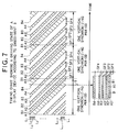
- FIG. 7 is a timing chart showing driving states in a plurality of vertical synchronizing periods of a display apparatus according to Embodiment 3.
- scanning lines which are constituted of pixels S connected to one gate line G are represented as L1, L2, L3, ..., and L n .
- Embodiment 2 the above explanation described that one strip-shaped illuminated area constituted of two or more adjacent scanning lines L is moved from top to bottom in appearance in the display screen D, so that a moving image is displayed.
- Embodiment 3 a plurality of strip-shaped illuminating areas, each of them constituted of adjacent two or more scanning lines L, are moved from top to bottom in appearance in a display screen D, so that a moving image is displayed.
- the display screen D i.e., one field
- a gray scale display is provided by display control using the subfields.
- moving image information inputted from the outside via an information line Sdp is converted into an n-bit (4 bits in FIG. 7) data signal by a display controller, so that 2 n -level gray scale is displayed.
- the display period of one field is constituted of four subfields SF1 to SF4 in Embodiment 3 below.
- a gate signal permits the selection of the scanning lines L which include the pixels S having the light-emitting devices E to be illuminated in the subfield SF1. Subsequently, among the pixels S arranged on the selected scanning lines L, the data signal is supplied, in the subfield SF1, line-sequentially to the pixels S including the light-emitting devices E to be actually illuminated, so that capacitors C are charged.
- a solid line "A1" indicates a change in the timing of starting the illuminating operation on each of the scanning lines L constituting the subfield SF1.
- the illuminating operation is started immediately after the pixels S to be illuminated are selected line-sequentially and the charging of the corresponding capacitors C is completed.
- the illuminating operation is started in the subfield SF1, according to the circuit configuration of the pixel S of FIG. 2, the illuminating operation is continued for equal illuminating period on each of the scanning lines L until an extinguishing operation (described later) is performed in the subfield SF1 as shown in FIG. 7.
- the extinguishing operation for the subfield SF1 is started on the currently illuminated light-emitting devices E for each of the scanning lines L having the illuminated pixels S.
- the extinguishing operation is performed in the order of stating the illuminating operation (the order indicated by the solid line A1).
- the gate signal permits the selection of the scanning line L which includes the pixels S having the light-emitting devices E to be extinguished in the subfield SF1. Subsequently, among the pixels S arranged on the selected scanning line L, an extinguishing signal (not shown) is line-sequentially supplied to the pixels S including the light-emitting devices E to be extinguished, so that the illuminating operation performed on the light-emitting devices E is stopped. Thus, the extinguishing operation is line-sequentially performed on the light-emitting devices E.
- a broken line "B1" indicates a change in the timing of starting the extinguishing operation on each of the scanning lines L after the illuminating operation is started on the light-emitting devices E in the subfield SF1 for each of the scanning lines L at the timing of the solid line A1.
- the extinguishing operation is started line-sequentially on each of the illuminated pixels S on the scanning lines L.
- the extinguishing state is maintained until another illuminating operation is started for each of the scanning lines L in the subsequent subfield SF2.
- the gate signal permits, based on the moving image information, the selection of the scanning lines L which include the pixels S having the light-emitting devices E to be illuminated in the subfield SF2. Thereafter, the light-emitting devices E are illuminated line-sequentially in the subfield SF2 as in the subfield SF1.
- a solid line "A2" indicates a change in the timing of starting the illuminating operation on each of the scanning lines L constituting the subfield SF2.
- the illuminating operation is continued for equal illuminating period on each of the scanning lines L until an extinguishing operation (described later) is performed on the subfield SF2 as shown in FIG. 7.
- the illuminating period of the subfield SF2 is twice that of the subfield SF1.
- the extinguishing operation for the subfield SF2 is performed on the currently illuminated light-emitting devices E line-sequentially on the scanning lines L having the illuminated pixels S.
- the extinguishing operation is performed in the order of stating the illuminating operation (the order indicated by the solid line A2).
- a broken line "B1" indicates a change in the timing of starting the extinguishing operation on each of the scanning lines L after the illuminating operation for the subfield SF2 is started on the light-emitting devices E for each of the scanning lines L at the timing of the solid line A2.
- the extinguishing operation is started line-sequentially on each of the illuminated pixels S on the scanning lines L.
- the extinguishing state is maintained until another illuminating operation is started for each of the scanning lines L in the subsequent subfield SF3.
- the gate signal permits, based on the moving image information, the selection of the scanning lines L which include the pixels S having the light-emitting devices E to be illuminated in the subfield SF3. Thereafter, the illuminating operation for the light-emitting devices E is performed line-sequentially in the subfield SF3 as in the subfields SF1 and SF2.
- a solid line "A3" indicates a change in the timing of starting the illuminating operation on each of the scanning lines L constituting the subfield SF3.
- the illuminating operation is continued for equal illuminating period on each of the scanning lines L until an extinguishing operation is performed on the subfield SF3 as shown in FIG. 7.
- the illuminating period of the subfield SF3 is twice that of the subfield SF2.
- the extinguishing operation for the subfield SF3 is performed on the currently illuminated light-emitting devices E line-sequentially on the scanning lines L having the illuminated pixels S.
- the extinguishing operation is performed in the order of stating the illuminating operation (the order indicated by the solid line A3).
- a broken line "B3" indicates a change in the timing of starting the extinguishing operation on each of the scanning lines L after the illuminating operation for the subfield SF3 is started on the light-emitting devices E at the timing of the solid line A2 for each of the scanning lines L.
- the extinguishing operation is started line-sequentially on each of the illuminated pixels S on the scanning lines L.
- the extinguishing state is maintained until another illuminating operation is started for each of the scanning lines L in the subsequent subfield SF4.
- the illuminating period of the subfield SF4 is twice that of the subfield SF3.
- image display is completed in one vertical synchronizing period.
- the light-emitting devices E are illuminated on the scanning lines L included in the subfields SF1 to SF4 and the light-emitting devices E are extinguished on the scanning lines L included in areas other than the subfields SF1 to SF4, for example, at timing T of FIG. 7 in the display screen D during one vertical synchronizing period.
- the light-emitting devices E are driven to display an image only during the illuminating period shorter than the vertical synchronizing period.
- the influence of an afterimage in human vision it is possible to reduce the influence of an afterimage in human vision and control the display of a fast moving image with higher quality.
- Selection writing scanning (scanning performed at the timing indicated by the solid lines A1, A2, A3, and A4 in FIG. 7) is performed in each of the subfields SF to place the pixels S on the corresponding scanning lines L into an image display state based on moving image information.
- a non-display scanning (scanning performed at the timing indicated by the broken lines B1, B2, B3, and B4 in FIG. 7) is performed to place into an image non-display state all the pixels S on the scanning lines L to be subjected to the selection writing scanning.
- Embodiment 3 described that the light-emitting devices E are driven so that the scanning lines L included in the subfields SF to be scanned during the vertical synchronizing period are simply reduced in number along the vertical synchronizing direction.
- the same effect as the display apparatus of Embodiment 3 can be obtained by driving the light-emitting devices E are driven so that the scanning lines L included in the subfields SF to be scanned during the vertical synchronizing period are simply increased along the vertical synchronizing direction.
- an image is displayed by driving the light-emitting devices E of the pixels S only during the illuminating period shorter than the vertical synchronizing period.
- selection writing scanning (scanning performed at the timing indicated by the solid lines A1, A2, A3, and A4 in FIG. 7) is performed in each of the subfields SF to place the pixels S on the corresponding scanning lines L into an image display state based on the moving image information, and before the selection writing scanning is started on the scanning lines L, a non-display scanning (scanning performed at the timing indicated by the broken lines B1, B2, B3, and B4 in FIG. 7) is performed to place into an image non-display state all the pixels S on the scanning lines L to be subjected to the selection writing scanning.
- a non-display scanning (scanning performed at the timing indicated by the broken lines B1, B2, B3, and B4 in FIG. 7) is performed to place into an image non-display state all the pixels S on the scanning lines L to be subjected to the selection writing scanning.
- Embodiment 3 described that gray scale display is provided according to a length of the illuminating period on the assumption that the light-emitting device only performs a binary operation of illumination and extinguishment.
- the present application is also applicable to the case where the light-emitting intensity of the light-emitting device is changed according to an input video signal in an analog fashion to provide gray scale display. Further, the present application is also applicable to the case where the light-emitting intensity of the light-emitting device is changed in an analog fashion in each of the subfields to provide gray scale display.
Landscapes
- Engineering & Computer Science (AREA)
- Physics & Mathematics (AREA)
- Computer Hardware Design (AREA)
- General Physics & Mathematics (AREA)
- Theoretical Computer Science (AREA)
- Control Of Indicators Other Than Cathode Ray Tubes (AREA)
- Liquid Crystal (AREA)
- Electroluminescent Light Sources (AREA)
- Liquid Crystal Display Device Control (AREA)
- Control Of El Displays (AREA)
Applications Claiming Priority (2)
| Application Number | Priority Date | Filing Date | Title |
|---|---|---|---|
| JP2002338405A JP2004170807A (ja) | 2002-11-21 | 2002-11-21 | 表示制御装置、表示システム及び表示制御方法 |
| JP2002338405 | 2002-11-21 |
Publications (2)
| Publication Number | Publication Date |
|---|---|
| EP1429311A2 true EP1429311A2 (de) | 2004-06-16 |
| EP1429311A3 EP1429311A3 (de) | 2007-12-26 |
Family
ID=32321891
Family Applications (1)
| Application Number | Title | Priority Date | Filing Date |
|---|---|---|---|
| EP03257271A Withdrawn EP1429311A3 (de) | 2002-11-21 | 2003-11-18 | Anzeigesteuerungsvorrichtung, Anzeigesystem und Anzeigesteuerungsverfahrung |
Country Status (3)
| Country | Link |
|---|---|
| US (1) | US7176872B2 (de) |
| EP (1) | EP1429311A3 (de) |
| JP (1) | JP2004170807A (de) |
Families Citing this family (7)
| Publication number | Priority date | Publication date | Assignee | Title |
|---|---|---|---|---|
| US7742019B2 (en) * | 2002-04-26 | 2010-06-22 | Toshiba Matsushita Display Technology Co., Ltd. | Drive method of el display apparatus |
| JP4646187B2 (ja) * | 2004-02-12 | 2011-03-09 | 東北パイオニア株式会社 | 発光ディスプレイ装置およびその駆動制御方法 |
| KR100748739B1 (ko) * | 2005-01-28 | 2007-08-13 | 도시바 마쯔시따 디스플레이 테크놀로지 컴퍼니, 리미티드 | El 표시 장치 및 해당 el 표시 장치의 구동 방법 |
| WO2018126463A1 (en) * | 2017-01-08 | 2018-07-12 | Viewtrix Technology Co., Ltd | Asynchronous control of display update and light emission |
| CN109661088A (zh) * | 2019-01-24 | 2019-04-19 | 欧普照明股份有限公司 | 一种智能照明图案控制方法、控制设备及系统 |
| JP7289205B2 (ja) * | 2019-03-07 | 2023-06-09 | シナプティクス インコーポレイテッド | 表示ドライバ、表示装置及び自発光表示パネルの制御方法 |
| CN117528873B (zh) * | 2024-01-04 | 2024-04-02 | 深圳市智岩科技有限公司 | 氛围灯设备及发光分区布局生成方法、装置和计算机设备 |
Family Cites Families (4)
| Publication number | Priority date | Publication date | Assignee | Title |
|---|---|---|---|---|
| US5805130A (en) * | 1994-04-27 | 1998-09-08 | Sharp Kabushiki Kaisha | Liquid crystal display device and method for driving the same |
| WO2002063384A1 (en) * | 2001-02-05 | 2002-08-15 | Matsushita Electric Industrial Co., Ltd. | Liquid crystal display unit and driving method therefor |
| JP2002244617A (ja) * | 2001-02-15 | 2002-08-30 | Sanyo Electric Co Ltd | 有機el画素回路 |
| KR100401377B1 (ko) * | 2001-07-09 | 2003-10-17 | 엘지.필립스 엘시디 주식회사 | 액정표시장치 및 그의 구동방법 |
-
2002
- 2002-11-21 JP JP2002338405A patent/JP2004170807A/ja not_active Abandoned
-
2003
- 2003-11-13 US US10/705,832 patent/US7176872B2/en not_active Expired - Fee Related
- 2003-11-18 EP EP03257271A patent/EP1429311A3/de not_active Withdrawn
Also Published As
| Publication number | Publication date |
|---|---|
| JP2004170807A (ja) | 2004-06-17 |
| EP1429311A3 (de) | 2007-12-26 |
| US20040100429A1 (en) | 2004-05-27 |
| US7176872B2 (en) | 2007-02-13 |
Similar Documents
| Publication | Publication Date | Title |
|---|---|---|
| US10818237B2 (en) | Organic light-emitting diode display device for improving image quality by turning off an OLED | |
| US9672769B2 (en) | Display apparatus and method of driving the same | |
| US10043448B2 (en) | Driving system for active-matrix displays | |
| CN101779229B (zh) | 显示装置及其驱动方法 | |
| US10083656B2 (en) | Organic light-emitting diode (OLED) display panel, OLED display device and method for driving the same | |
| US8139002B2 (en) | Organic light emitting diode display and driving method thereof | |
| US8063858B2 (en) | Active matrix display apparatus and driving method therefor | |
| JP6764829B2 (ja) | 表示パネルの制御装置、表示装置および表示パネルの駆動方法 | |
| JP2002169499A (ja) | 表示パネルの駆動方法及び表示パネルの駆動制御装置 | |
| CN112863434B (zh) | 控制方法以及控制装置 | |
| CN100524417C (zh) | 有机电致发光显示器件及其驱动方法 | |
| JP2002169509A (ja) | 平面表示パネルの駆動方法及び有機エレクトロルミネッセンス表示パネルの駆動方法 | |
| JP2003223136A (ja) | 表示装置およびその駆動方法 | |
| JP2008122892A (ja) | 有機電界発光表示装置の駆動方法 | |
| US20090284502A1 (en) | Image signal display control apparatus and image signal display control method | |
| US7623102B2 (en) | Active matrix type display device | |
| US7176872B2 (en) | Display controller, display system, and display controlling method | |
| US8004612B2 (en) | Apparatus and method for controlling display brightness in an image display device | |
| JP2011022462A (ja) | 表示装置およびその駆動方法ならびに電子機器 | |
| KR100659622B1 (ko) | 표시 장치 | |
| JP2004309844A (ja) | 電気光学装置、電気光学装置の駆動方法電気光学装置の駆動回路および電子機器 | |
| JP2002287682A (ja) | 表示パネルとその駆動方法 | |
| JP2011022239A (ja) | 表示装置およびその駆動方法ならびに電子機器 | |
| KR102363845B1 (ko) | 유기 발광 다이오드 표시 장치 및 그 센싱 방법 | |
| JP2001092410A (ja) | El表示装置の駆動装置及び階調表示方法 |
Legal Events
| Date | Code | Title | Description |
|---|---|---|---|
| PUAI | Public reference made under article 153(3) epc to a published international application that has entered the european phase |
Free format text: ORIGINAL CODE: 0009012 |
|
| AK | Designated contracting states |
Kind code of ref document: A2 Designated state(s): AT BE BG CH CY CZ DE DK EE ES FI FR GB GR HU IE IT LI LU MC NL PT RO SE SI SK TR |
|
| AX | Request for extension of the european patent |
Extension state: AL LT LV MK |
|
| PUAL | Search report despatched |
Free format text: ORIGINAL CODE: 0009013 |
|
| AK | Designated contracting states |
Kind code of ref document: A3 Designated state(s): AT BE BG CH CY CZ DE DK EE ES FI FR GB GR HU IE IT LI LU MC NL PT RO SE SI SK TR |
|
| AX | Request for extension of the european patent |
Extension state: AL LT LV MK |
|
| AKX | Designation fees paid | ||
| REG | Reference to a national code |
Ref country code: DE Ref legal event code: 8566 |
|
| STAA | Information on the status of an ep patent application or granted ep patent |
Free format text: STATUS: THE APPLICATION IS DEEMED TO BE WITHDRAWN |
|
| 18D | Application deemed to be withdrawn |
Effective date: 20080603 |