EP1426430A1 - Plasma-anzeigevorrichtung, fluoreszierendes material und dessen herstellung - Google Patents
Plasma-anzeigevorrichtung, fluoreszierendes material und dessen herstellung Download PDFInfo
- Publication number
- EP1426430A1 EP1426430A1 EP02765480A EP02765480A EP1426430A1 EP 1426430 A1 EP1426430 A1 EP 1426430A1 EP 02765480 A EP02765480 A EP 02765480A EP 02765480 A EP02765480 A EP 02765480A EP 1426430 A1 EP1426430 A1 EP 1426430A1
- Authority
- EP
- European Patent Office
- Prior art keywords
- phosphor
- blue
- mgal
- mixed solution
- luminance
- Prior art date
- Legal status (The legal status is an assumption and is not a legal conclusion. Google has not performed a legal analysis and makes no representation as to the accuracy of the status listed.)
- Granted
Links
Images


Classifications
-
- C—CHEMISTRY; METALLURGY
- C09—DYES; PAINTS; POLISHES; NATURAL RESINS; ADHESIVES; COMPOSITIONS NOT OTHERWISE PROVIDED FOR; APPLICATIONS OF MATERIALS NOT OTHERWISE PROVIDED FOR
- C09K—MATERIALS FOR MISCELLANEOUS APPLICATIONS, NOT PROVIDED FOR ELSEWHERE
- C09K11/00—Luminescent, e.g. electroluminescent, chemiluminescent materials
- C09K11/08—Luminescent, e.g. electroluminescent, chemiluminescent materials containing inorganic luminescent materials
- C09K11/64—Luminescent, e.g. electroluminescent, chemiluminescent materials containing inorganic luminescent materials containing aluminium
-
- H—ELECTRICITY
- H01—ELECTRIC ELEMENTS
- H01J—ELECTRIC DISCHARGE TUBES OR DISCHARGE LAMPS
- H01J11/00—Gas-filled discharge tubes with alternating current induction of the discharge, e.g. alternating current plasma display panels [AC-PDP]; Gas-filled discharge tubes without any main electrode inside the vessel; Gas-filled discharge tubes with at least one main electrode outside the vessel
- H01J11/20—Constructional details
- H01J11/34—Vessels, containers or parts thereof, e.g. substrates
- H01J11/42—Fluorescent layers
-
- C—CHEMISTRY; METALLURGY
- C09—DYES; PAINTS; POLISHES; NATURAL RESINS; ADHESIVES; COMPOSITIONS NOT OTHERWISE PROVIDED FOR; APPLICATIONS OF MATERIALS NOT OTHERWISE PROVIDED FOR
- C09K—MATERIALS FOR MISCELLANEOUS APPLICATIONS, NOT PROVIDED FOR ELSEWHERE
- C09K11/00—Luminescent, e.g. electroluminescent, chemiluminescent materials
- C09K11/08—Luminescent, e.g. electroluminescent, chemiluminescent materials containing inorganic luminescent materials
- C09K11/77—Luminescent, e.g. electroluminescent, chemiluminescent materials containing inorganic luminescent materials containing rare earth metals
- C09K11/7728—Luminescent, e.g. electroluminescent, chemiluminescent materials containing inorganic luminescent materials containing rare earth metals containing europium
- C09K11/7734—Aluminates
-
- H—ELECTRICITY
- H01—ELECTRIC ELEMENTS
- H01J—ELECTRIC DISCHARGE TUBES OR DISCHARGE LAMPS
- H01J1/00—Details of electrodes, of magnetic control means, of screens, or of the mounting or spacing thereof, common to two or more basic types of discharge tubes or lamps
- H01J1/54—Screens on or from which an image or pattern is formed, picked-up, converted, or stored; Luminescent coatings on vessels
- H01J1/62—Luminescent screens; Selection of materials for luminescent coatings on vessels
- H01J1/63—Luminescent screens; Selection of materials for luminescent coatings on vessels characterised by the luminescent material
-
- H—ELECTRICITY
- H01—ELECTRIC ELEMENTS
- H01J—ELECTRIC DISCHARGE TUBES OR DISCHARGE LAMPS
- H01J11/00—Gas-filled discharge tubes with alternating current induction of the discharge, e.g. alternating current plasma display panels [AC-PDP]; Gas-filled discharge tubes without any main electrode inside the vessel; Gas-filled discharge tubes with at least one main electrode outside the vessel
- H01J11/10—AC-PDPs with at least one main electrode being out of contact with the plasma
- H01J11/12—AC-PDPs with at least one main electrode being out of contact with the plasma with main electrodes provided on both sides of the discharge space
Definitions
- the present invention relates to a plasma display apparatus(device) used for image display on a television or other equipment. It also relates to a phosphor for use in the plasma display device, and a method of fabricating the phosphor(fluorescent material).
- a display device using a plasma display panel (hereinafter referred to as a "PDP") has recently been drawing attention, as a large, thin, and light color display device.
- a plasma display device using a PDP performs additive color mixing of so-called three primary colors (red, green, and blue) to provide full-color display.
- a plasma display device has phosphor layers for emitting the respective three primary colors, i.e. red (R), green (G), and blue (B). Phosphor particles constituting these phosphor layers are exited by ultraviolet light generated in discharge cells of the PDP to generate visible light of respective colors.
- Known as compounds used for the phosphors of above respective colors are (YGd)BO 3 :Eu 3+ and Y 2 O 3 :Eu 3+ for red emission, Zn 2 SiO 4 :Mn 2+ for green emission, and BaMaAl 10 O 17 :Eu 2+ for blue emission.
- Each of these phosphors is fabricated by mixing specific materials and firing the mixture at high temperatures of at least 1,000 °C for solid-phase reaction (see "Phosphor Handbook" p.219 and 225, Ohmsha, for example). The phosphor particles obtained by this firing are used after they are milled and classified (average diameter of red and green particles: 2 to 5 ⁇ m, average diameter of blue particles: 3 to 10 ⁇ m).
- the phosphor particles are milled and classified for the following reason.
- a technique of screen-printing a paste of phosphor particles of each color is used.
- the smaller and more uniform diameters of phosphor particles i.e. a uniform particle size distribution
- the coated surface is smoother.
- the smoother coated surface increases the packing density of the phosphor particles in a phosphor layer and the emission surface area of the particles, thus alleviating unstableness at address drive. As a result, it is theoretically considered that the luminance of the plasma display device can be increased.
- the present invention aims to inhibit water adsorption onto the surface of a blue phosphor, decrease luminance degradation and chromaticity shift of a phosphor, or improve discharge characteristics thereof.
- elimination of oxygen vacancy in the vicinity of a layers containing Ba atoms (Ba-O layers) in a blue phosphor inhibits water adsorption onto the surface of the blue phosphor, decreases luminance degradation and chromaticity shift of a phosphor, or improves discharge characteristics thereof.
- a plasma display device of the present invention has a plasma display panel in which a plurality of discharge cells of one or a plurality of colors are disposed in arrays, phosphor layers having a color corresponding to the respective discharge cells are disposed, and the phosphor layers are excited by ultraviolet light to emit light.
- the phosphor layers have a blue phosphor.
- the blue phosphor is made of a compound represented by Ba 1-x MgAl 10 O 17 :Eu x or Ba 1-x-y Sr y MgAl 10 O 17 :Eu x in which at least one kind of the elements Ti, Zr, Hf, Si, Ge, Sn and Ce substitutes for part of the element Al or Mg.
- a phosphor of the present invention is a blue phosphor having a crystal structure of Ba 1-x MgAl 10 O 17 :Eu x or Ba 1-x-y Sr y MgAl 10 O 17 :Eu x that is exited by ultraviolet light to emit visible light.
- a quadrivalent element substitutes for the element Al or Mg that constitutes the phosphor.
- a method of manufacturing a phosphor of the present invention includes: a mixed solution fabrication step in which a metal salt or organometalic salt containing elements constituting a blue phosphor (Ba, Mg, Al, Eu, and M (where M is one kind of the elements Ti, Zr, Si, Ge, Sn and Ce )) is mixed with an aqueous medium to fabricate a mixed solution; and a step of drying the mixed solution, and thereafter firing the mixture in a reducing atmosphere to fabricate Ba 1-x (Mg 1-a M a )(Al 1-b M b )Al 10 O 17 :Eu x and Ba 1-x-y Sr y (Mg 1-a M a )(Al 1-b M b )Al 10 O 17 (where M is at least one kind of the elements Ti, Zr, Hf, Si, Ge, Sn and Ce ).
- a metal salt or organometalic salt containing elements constituting a blue phosphor Ba, Mg, Al, Eu, and
- a phosphor for use in a PDP or other equipment is fabricated by a solid-phase reaction method, an aqueous solution reaction method, or other methods.
- a phosphor has smaller particle diameters, defects are likely to occur.
- milling a phosphor after firing leads many defects.
- ultraviolet light having a wavelength of 147 nm generated by discharge in driving a panel causes defects in a phosphor (see Electronic Information and Communication Institute, Technical Research Report, EID99-94, January 27, 2000, for example).
- Fig. 6 is a diagram schematically showing a structure of a Ba-O layer in the blue phosphor BaMaAl 10 O 17 :Eu.
- defects are caused by impact of ions generated in driving a panel on the phosphor and by ultraviolet light having a wavelength of 147 nm.
- the inventors have found that the luminance degradation is not only essentially caused by existence of the defects but is caused by selective adsorption of water or carbonic acid gas to oxygen (O) vacancy in the vicinity of a Ba-O layer.
- O oxygen
- the phosphor reacts with water, thus causing luminance degradation and color shift.
- the inventors have come to know that adsorption of water or carbonic acid gas to oxygen vacancy in the vicinity of a Ba-O layer in a blue phosphor causes a various kinds of degradation.
- the inventors have decreased oxygen vacancy in the vicinity of a Ba-O layer in a blue phosphor to prevent degradation thereof in a panel manufacturing process and in driving a panel, without decreasing the luminance of the blue phosphor.
- the inventors have substitute a quadrivalent element for part of the element aluminum (Al) or magnesium (Mg) in a blue phosphor having a crystal structure of BaMgAl 10 O 17 :Eu or BaSrMgAl 10 O 17 :Eu.
- Positive electrical charges are increased in the crystal by substituting quadrivalent positive ions, such as titanium (Ti), zirconium (Zr), hafnium (Hf), silicon (Si), germanium (Ge), tin (Sn), and cerium (Ce), for any position in the trivalent or divalent ions.
- quadrivalent positive ions such as titanium (Ti), zirconium (Zr), hafnium (Hf), silicon (Si), germanium (Ge), tin (Sn), and cerium (Ce)
- negatively charged oxygen compensates for oxygen vacancy in the vicinity of the element Ba. As a result, it is considered that the oxygen vacancy in the vicinity of the Ba-O layer can be decreased.
- a conventional solid-phase firing method As methods of manufacturing a phosphor itself, a conventional solid-phase firing method, a liquid-phase method, and a liquid spray method are considered.
- oxide or carbonate materials are fired using a fluxing agent.
- a precursor of a phosphor is fabricated using a coprecipitation method of hydrolyzing an organometallic salt or a nitrate in an aqueous solution or forming precipitation by addition of an alkali, and then the precursor is heat-treated.
- an aqueous solution containing phosphor materials is sprayed into a high-temperature furnace.
- Carbonates and oxides such as BaCO 3 , MgCO 3 , Al 2 O 3 , Eu 2 O 3 , and MO 2 (where M is Ti, Zr, Hf, Si, Ge, Sn, or Ce), as materials, are mixed with a small amount of fluxing agent (AlF 3 or BaCl 2 ) as a sintering agent.
- the mixture is fired at a temperature of 1,400 °C for two hours.
- the fired mixture is milled and classified.
- the milled and classified product is fired at a temperature of 1,500 °C for two hours in a reducing atmosphere (H 2 (5%) - N 2 matrix), and milled and classified again to provide a phosphor.
- organometallic salts containing elements constituting the phosphor such as alkoxide and acetylacetone, or nitrates are dissolved in water, and then a co-precipitate (hydrate) is obtained by hydrolysis.
- the hydrate is hydro-thermally synthesized (crystallized in an autoclave), fired in air, or sprayed into a high-temperature furnace to provide fine particles.
- the fine particles are fired at a temperature of 1,500 °C for two hours in a reducing atmosphere (H 2 (5%) - N 2 matrix) to provide a phosphor.
- the blue phosphor obtained in this method is milled and classified to provide a phosphor.
- the substitution value of quadrivalent ions (Ti, Zr, Hf, Si, Sn, Ge, or Ce) substituting for Al or Mg ions ranges from 0.01 to 3% of Al or Mg.
- the substitution value up to 0.01 % the effect of preventing luminance degradation is small.
- the quadrivalent ions have substituted for Al or Mg ions instead of Ba or Eu ions because the blue emission spectrum has a wavelength of 450 nm at any substitution value.
- substituting quadrivalent ions for Al or Mg ions in a crystal of BaMgAl 10 O 17 :Eu using the conventional method of fabricating blue phosphor particles can provide a phosphor resistant to water (i.e. durable against water and carbonic acid gas generated in a phosphor firing process, panel sealing process, panel aging process, or in driving a panel) without degradation of the luminance of the blue phosphor.
- a plasma display device of the present invention has a PDP in which a plurality of discharge cells of one or a plurality of colors are disposed in arrays, phosphor layers having a color corresponding to the respective discharge cells are disposed, and the phosphor layers are excited by ultraviolet light to emit light.
- Each of the blue phosphor layer is characterized by being made of blue phosphor particles in which quadrivalent ions (Ti, Zr, Hf, Si, Sn, Ge, or Ce) substitute for Al or Mg ions in a crystal of BaMgAl 10 O 17 :Eu or BaSrMgAl 10 O 17 :Eu x that has a uniform particle size distribution.
- the diameters of blue phosphor particles in which quadrivalent ions (Ti, Zr, Hf, Si, Sn, Ge, or Ce) substitute for part of Al or Mg ions in BaMgAl 10 O 17 :Eu or BaSrMgAl 10 O 17 :Eu are as small as 0.05 to 3 ⁇ m.
- the particle size distribution of the blue particles is excellent.
- the packing density of the layer increases. This increases the emission area of phosphor particles substantially contributing to light emission.
- the increased emission area can increase the luminance of a plasma display device and provide a plasma display device that has inhibited luminance degradation and color shift and excellent luminance characteristics.
- the average particle diameter of phosphor particles ranges from 0.1 to 2.0 ⁇ m.
- the maximum particle size is at most four times of the mean value and the minimum value is at least a quarter of the mean value.
- the area ultraviolet light reaches is as shallow as several hundred nm from the surface of the particle and only the surface thereof emits light.
- the diameter of such a phosphor particle is 2.0 ⁇ m or smaller, the surface area of the particle contributing to light emission increases and the emission efficiency of the phosphor layer is kept high.
- the thickness of the phosphor must be at least 20 ⁇ m and a sufficient discharge space cannot be ensured.
- defects are likely to occur and the luminance does not increase.
- the thickness of a phosphor layer is set to 8 to 25 times of the average diameter of phosphor particles, a sufficient discharge space can be ensured while the emission efficiency of the phosphor layer is kept high. Therefore, the luminance of a plasma display device can be increased. Especially when the average particle diameter of a phosphor is up to 3 ⁇ m, this effect is greater (see The Institute of Image Information and Television Engineers, IDY2000-317, pp32).
- a specific example of phosphor particles used for blue phosphor layers in a plasma display device is made of a compound represented by Ba 1-x MgAl 10 O 17 :Eu x or Ba 1-x-y Sr y MgAl 10 O 17 :Eu x .
- values X and Y in these compounds are such that 0.03 ⁇ X ⁇ 0.20 and 0.1 ⁇ Y ⁇ 0.5, the blue phosphor layers have a high luminance. Thus, satisfying these conditions is preferable.
- a specific example of phosphor particles used for red phosphor layers in a plasma display device is made of a compound represented by Y 2-x O 3 :Eu x or (Y,Gd) 1-x BO 3 :Eu x.
- value X in the compounds of the red phosphor is such that 0.05 ⁇ X ⁇ 0.20, the red phosphor layers have an excellent luminance and resistance to luminance degradation. Thus, satisfying this condition is preferable.
- a specific example of phosphor particles used for green phosphor layers in a plasma display device is made of a compound represented by Ba 1-x Al 12 O 19 :Mn x or Zn 2-x SiO 4 :Mn x .
- value X in the compounds of the green phosphor is such that 0.01 ⁇ X ⁇ 0.10, the green phosphor layers have an excellent luminance and resistance to luminance degradation. Thus, satisfying this condition is preferable.
- a method of manufacturing a plasma display panel of the present invention is characterized by having a disposing step, firing step and sealing step.
- the disposing step pastes are disposed on a substrate of a first panel.
- Each kind of the pastes is made of phosphor particles in which quadrivalent ions substitute for Al or Mg ions in the blue phosphor Ba 1-x MgAl 10 O 17 :Eu x or Ba 1-x-y Sr y MgAl 10 O 17 :Eu x , red phosphor particles, or green phosphor particles, and a binder.
- the firing step the binder included in each kind of the pastes disposed on the first panel is burnt out.
- the sealing step the first panel having the phosphor particles disposed on the substrate by the firing step, and a second panel are placed one on the other, and sealed.
- the phosphor of the present invention can also be applied to fluorescent lighting.
- the fluorescent lighting is characterized by having a phosphor layer that is excited by ultraviolet light to emit visible light, and the phosphor layer is made of phosphor particles each having water repellent finish on the surface thereof.
- This structure can provide fluorescent lighting that has phosphor particles having excellent light emission characteristics, luminance, and resistance to luminance degradation.
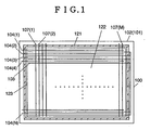
- Fig. 1 is a schematic plan view of a PDP with a front glass substrate thereof removed.
- Fig. 2 is a partially sectional view in perspective of an image display area of the PDP.
- the number of display electrodes, display scan electrodes, and address electrodes is reduced to facilitate explanation.
- the structure of a PDP is described.
- PDP 100 includes front glass substrate 101 (not shown), rear glass substrate 102, N display electrodes 103, N display scan electrodes 104 (Nth electrode indicated by N), M address electrodes 107 (Mth electrode indicated by M), and hermetic seal layer 121 shown by oblique lines.
- the PDP has an electrode matrix having a three-electrode structure made of respective electrodes 103, 104, and 107. Respective cells are formed at the respective intersections of display scan electrodes 104 and address electrodes 107.
- this PDP 100 is structured so that a front panel and a rear panel are assembled together and discharge space 122 formed between the front panel and the rear panel is filled with a discharge gas.
- display electrodes 103, display scan electrodes 104, dielectric glass layer 105, and MgO protective layer 106 are disposed on a principal surface of front glass substrate 101.
- address electrodes 107, dielectric glass layer 108, barrier ribs 109, and phosphor layers 110R, 110G and 110B are disposed on a principal surface of rear glass substrate 102.
- phosphor layers 110B a quadrivalent element substitutes for the element Al or Mg in a blue phosphor.
- display driver circuit 153 When an image is displayed on a plasma display device, first, display driver circuit 153, display scan driver circuit 154, and address driver circuit 155 are connected to PDP 100, as shown Fig. 3. Next, according to control of controller 152, a signal voltage is applied across display scan electrode 104 and address electrode 107 of a cell to be lit for address discharge therebetween. Then, a pulse voltage is applied across display electrode 103 and display scan electrode 104 for sustain discharge. This sustain discharge generates ultraviolet light in the cell. The phosphor layer excited by this ultraviolet light emits light, thus lighting the cell. Combination of lit and unlit cells of the respective colors provides image display.
- N display electrodes 103 and N display scan electrodes 104 are arranged on front glass substrate 101 alternately, in parallel with each other, like stripes. (In Fig. 2, only two of respective electrodes are shown for simplicity.) Thereafter, the electrodes are covered with dielectric glass layer 105, and MgO protective layer 106 is further formed over the surface of dielectric glass layer 105.
- Display electrodes 103 and display scan electrodes 104 are made of silver. These electrodes are formed by applying a silver paste for electrodes by screen-printing and firing the paste.
- Dielectric glass layer 105 is formed by applying a paste containing lead glass material by screen-printing, and firing the paste at a specified temperature for a specified period of time (e.g. at 56 °C for 20 min.) so that the layer has a specified thickness (approx. 20 ⁇ m).
- a paste containing lead glass material to be used include a mixture of PbO (70 wt%), B 2 O 3 (15 wt%), SiO 2 (10 wt%), Al 2 O 3 (5 wt%) and an organic binder ( ⁇ -terpineol containing 10 % of ethyl cellulose dissolved therein).
- the organic binder contains a resin dissolved in an organic solvent.
- Acrylic resin can be used as a resin other than the ethyl cellulose, and n-butylcarbitol as an organic solvent.
- a dispersion agent e.g. glyceryl trileate
- glyceryl trileate can be mixed into such an organic binder.
- MgO protective layer 106 is made of magnesium oxide (MgO).
- the layer is formed by sputtering method or chemical vapor deposition (CVD) method, for example, to have a specified thickness (approx. 0.5 ⁇ m).
- M address electrodes 107 are formed in lines by screen-printing a silver paste for electrodes on rear glass substrate 102 and firing the paste.
- dielectric glass layer 108 is formed by applying a paste containing lead glass material to the address electrodes by a screen-printing method.
- Barrier ribs 109 are formed by repeatedly applying the same paste containing lead glass material to the dielectric glass layer by the screen-printing method at a specified pitch and firing the paste. These barrier ribs 109 partition discharge space 122 into respective cells (unit emission area) in the direction of the lines.
- Fig. 4 is a partially sectional view of PDP 100. As shown in the drawing, interval dimension W between barrier ribs 109 is specified to a value ranging from approx. 130 to 240 ⁇ m, according to a HDTV screen having a diagonal size ranging from 32 to 50 in.
- Paste-like phosphor ink made of red (R), green (G), or blue (B) phosphor particles and an organic binder is applied to grooves between barrier ribs 109, and fired at temperatures ranging from 400 to 590 °C to burn out the organic binder.
- phosphor layers 110R, 110G, and 110B in which phosphor particles of corresponding colors are bound are formed.
- quadrivalent element ions substitute for Al or Mg element ions in Ba 1-x MgAl 10 O 17 :Eu x or Ba 1-x-y Sr y MgAl 10 O 17 :Eu x .
- each of these phosphor layers 110R, 110G, and 110B on address electrode 107 in the direction of lamination is approx. 8 to 25 times of the average diameter of the phosphor particles of each color.
- the phosphor layer needs to absorb ultraviolet light generated in the discharge space instead of allowing it to pass through.
- the phosphor layer has a thickness in which at least eight layers, preferably, approx. 20 layers are laminated. For a thickness larger than that, the emission efficiency of the phosphor layer is almost saturated. Further, for a thickness exceeding lamination of approx. 20 layers, sufficiently large discharge space 122 cannot be ensured.
- Phosphor particles having sufficiently small diameters and spherical shapes like those obtained by hydrothermal synthesis or other methods, have a packing factor of the phosphor layer and a total surface area of the phosphor particles larger than those of phosphor particles having non-spherical shapes, even when the number of laminated layers are the same.
- the surface areas thereof contributing to actual light emission of the phosphor layer are increased and the emission efficiency is further increased. Descriptions are given later of a method of synthesizing these phosphor layers 110R, 110G, and 110B, and a method of fabricating blue phosphor particles for use in the blue phosphor layer employing substitution of quadrivalent ions.
- the front panel and the rear panel produced in this manner are placed one on the other so that respective electrodes on the front panel are orthogonal to the address electrodes on the rear panel.
- a sealing glass is inserted between the panels in the periphery thereof and fired at a temperature of approx. 450 °C for 10 to 20 min., for example, to from hermetical seal layer 121 (see Fig. 1) for sealing.
- discharge space 122 is once evacuated to a high vacuum (e.g. 1.1 ⁇ 10 -4 Pa) and filled with a discharge gas (e.g. He-Xe or Ne-Xe inert gas) at a specified pressure, to provide PDP 100.
- a high vacuum e.g. 1.1 ⁇ 10 -4 Pa
- a discharge gas e.g. He-Xe or Ne-Xe inert gas
- Fig. 5 is a schematic diagram showing a structure of ink dispenser 200 for use in forming phosphor layers 110R, 110G, and 110B.
- ink dispenser 200 includes server 210, pressure pump 220, and header 230.
- Phosphor ink is pressurized by pressure pump 220 and supplied from server 210 for storing the phosphor ink to header 230.
- the ink dispenser is structured so that header 230 has ink chamber 230a and nozzle 240, and the phosphor ink pressurized and supplied to ink chamber 230a is continuously ejected from nozzle 240. It is desirable that bore diameter D of this nozzle 240 is set to at least 30 ⁇ m in order to prevent clogging of the nozzle. It is also desirable that bore diameter D is equal to or smaller than interval W between barrier ribs 109 (approx. 130 to 200 ⁇ m) in order to prevent displacement of a phosphor layer from the barrier ribs in application. Thus, bore diameter D is generally set to 30 to 130 ⁇ m.
- Header 230 is structured to be driven lineally by a header scanning mechanism (not shown). Continuously ejecting phosphor ink 250 from nozzle 240 and scanning header 230 at the same time allows the phosphor ink to be uniformly applied to the grooves between barrier ribs 109 on rear glass substrate 102. Viscosity of the phosphor ink used in this embodiment is kept within the range of 1,500 to 3,000 centipoises (CP) at a temperature of 25 °C.
- CP centipoises
- This server 210 also has a mixer (not shown). Mixing prevents precipitation of particles in phosphor ink.
- Header 230 is integrally formed with ink chamber 230a and nozzle 240 by performing machining and electric discharge machining on a metallic material.
- the methods of forming phosphor layers are not limited to the above method.
- Other various kinds of usable methods include photolithography, screen-printing, and a method of disposing a film including phosphor particles mixed therein.
- the phosphor ink is prepared by mixing phosphor particles of each color, a binder and a solvent so that the mixture has a viscosity ranging from 1,500 to 3,000 centipoises (CP).
- a surface-active agent, silica, a dispersant agent (0.1 to 5 wt%) can also be added, as required.
- red phosphor included in this phosphor ink is a compound represented by (Y,Gd) 1-x BO 3 :Eu x or Y 2-x O 3 :Eu x .
- the element Eu substitutes for part of the element Y constituting the matrix of the compounds.
- the substitution value X of the element Eu with respect to the element Y is 0.05 ⁇ X ⁇ 0.20.
- the phosphor has a high luminance but considerable luminance degradation. For this reason, it is considered that the red phosphor cannot be used practically.
- the composition ratio of Eu mainly emitting light is small and thus the luminance decreases. Therefore, the red phosphor cannot be used as a phosphor.
- Used as a green phosphor is a compound represented by Ba 1-x Al 12 O 19 :Mn x or Zn 2-x SiO 4 :Mn x .
- Ba 1-x Al 12 O 19 :Mn x is a compound in which the element Mn substitutes for part of the element Ba constituting the matrix of the compound.
- Zn 2-x SiO 4 :Mn x is a compound in which the element Mn substitutes for part of the element Zn constituting the matrix of the compound. It is preferable that the substitution value X of the element Mn with respect to the elements Ba and Zn is 0.01 ⁇ X ⁇ 0.10 for the reason described in the case of the red phosphor.
- Ba 1-x MgAl 10 O 17 :Eu x or Ba 1-x-y Sr y MgAl 10 O 17 :Eu x are compounds in which the element Eu or Sr substitutes for part of the element Ba constituting the matrix of the compounds. It is preferable that the substitution value X of the element Eu and substitution value Y of the element Sr with respect to the element Ba are 0.03 ⁇ X ⁇ 0.20 and 0.1 ⁇ Y ⁇ 0.5, respectively, for the reason described in the above case.
- substitution values of quadrivalent ions (Ti, Zr, Hf, Si, Ge, Sn, or Ce) substituting for the element Al or Mg is 0.001 ⁇ a ⁇ 0.03 and 0.001 ⁇ b ⁇ 0.03, in Ba(Mg 1-a M a )(Al 1-b M b ) 10 O 17 :Eu x .
- substitution values ranges from 0.1 to 3%.
- Ethyl cellulose or acrylic resin can be used as a binder included in phosphor ink (in an amount of 0.1 to 10 wt% of the ink) and ⁇ -terpineol or n-butylcarbitol can be used as a solvent.
- Polymers, such as PMA and PVA, can also be used as a binder, and organic solvent, such as diethyleneglycol and methyl ether, can also be used as a solvent.
- the phosphor particles used in this embodiment are manufactured by a solid-phase firing method, aqueous solution reaction method, spray firing method, or hydrothermal synthesis method.
- This mixture is dissolved in an aqueous medium to provide a mixed solution.
- aqueous medium ion-exchange water or pure water is preferable because they contain no impurities.
- non-aqueous solvent e.g. methanol and ethanol
- nitrates, chlorides, or organic compounds of the quadrivalent ions used as materials for substituting quadrivalent ions (Ti, Zr, Hf, Si, Sn, Ge, or Ce) for Mg or Al are nitrates, chlorides, or organic compounds of the quadrivalent ions.
- substitution values of the materials the materials are mixed to provide 0.001 ⁇ a and b ⁇ 0.03 in (Mg 1-a M a )(Al 1-b M b ) where M is a quadrivalent ion.
- the hydrate mixed solution is held in a container made of a corrosion- and heat- resistant material, such as gold and platinum. Then the mixed solution is hydro-thermally synthesized for 12 to 20 hours, at specified temperatures (100 to 300 °C) under specified pressures (0.2 to 10 MPa), in a high pressure vessel, using equipment capable of heating and pressurizing at the same time, such as an autoclave.
- a corrosion- and heat- resistant material such as gold and platinum
- these particles are fired in a reducing atmosphere containing 5% of hydrogen and 95% of nitrogen, for example, at a specified temperature for a specified period of time (e.g. at 1,350 °C for two hours). Thereafter, the fired particles are classified to provide a desired blue phosphor, Ba 1-x MgAl 10 O 17 :Eu x , in which quadrivalent ions substitute for part of the elements Mg or Al.
- the phosphor particles obtained by hydrothermal synthesis have spherical shapes and an average particle diameter ranging from approx. 0.05 to 2.0 ⁇ m, which is smaller than that of particles fabricated by the conventional solid-phase reaction method.
- the term "spherical” as used herein is defined so that the aspect ratios (minor axis diameter/major axis diameter) of most of the phosphor particles range from 0.9 to 1.0, for example. Not all the phosphor particles need to fall within this range.
- the hydrate mixture can be sprayed from a nozzle into a high-temperature furnace to synthesize a phosphor instead of being held in a gold or platinum container.
- This method is known as a spray method and the blue phosphor can also be manufactured by the spray method.
- This phosphor is made of materials different from those of the above Ba 1-x MgAl 10 O 17 :Eu x , and fabricated by a solid reaction method. The materials used are described hereinafter.
- the materials i.e. barium hydroxide (Ba(OH) 2 ), strontium hydroxide (Sr(OH) 2 ), magnesium hydroxide (Mg(OH) 2 ), aluminum hydroxide (Al(OH) 3 ), and europium hydroxide (Eu(OH) 2 ) are weighted in a required molar ratio.
- oxides or hydroxides containing quadrivalent ions Ti, Zr, Hf, Si, Ge, Sn, or Ce
- These materials are mixed together with AlF 3 , a fluxing agent.
- the mixture is fired at specified temperatures (1,300 to 1400°C) for specified periods of time (12 to 20 hours.)
- Ba 1-x-y Sr y MgAl 10 O 17 :Eu x in which quadrivalent ions substitute for Mg or Al can be obtained.
- the average diameter of the phosphor particles obtained by this method ranges from approx. 0.1 to 3.0 ⁇ m.
- the phosphor is fired in a reducing atmosphere (containing 5% of hydrogen and 95% of nitrogen, for example) at specified temperatures (1,000 to 1,600°C) for two hours, and thereafter classified by an air classifier to provide phosphor particles.
- a reducing atmosphere containing 5% of hydrogen and 95% of nitrogen, for example
- specified temperatures 1,000 to 1,600°C
- an air classifier to provide phosphor particles.
- Mainly used as the materials of the phosphor are oxides, nitrates, and hydroxides.
- the phosphor can also be fabricated using organometallic compounds containing the elements Ba, Sr, Mg, Al, Eu, Ti, Zr, Hf, Si, Sn, Ge, and Ce, such as metal alkoxide and acethylacetone.
- This mixture is dissolved in ion-exchange water to provide a mixed solution.
- an aqueous base e.g. ammonia aqueous solution
- this hydrate and ion-exchange water is held in a capsule made of a corrosion- and heat-resistant material, such as platinum and gold.
- This solution is hydro-thermally synthesized at specified temperatures under specified pressures for specified periods of time (e.g. 100 to 300°C, 0.2 to 10 MPa, 2 to 20 hours) in a high pressure vessel, using an autoclave, for example.
- the phosphor obtained by this hydrothermal synthesis process has particle diameters ranging from approx. 0.1 to 2.0 ⁇ m and spherical shapes. Next, these particles are annealed in air at temperatures ranging from 800 to 1,100°C, and classified to provide the green phosphor.
- an aqueous base e.g. ammonia aqueous solution
- a hydrate is added to this mixed solution to provide a hydrate.
- this hydrate and ion-exchange water is held in a container made of a corrosion- and heat-resistant material, such as platinum and gold.
- This mixture is hydro-thermally synthesized at temperatures ranging from 100 to 300°C, under pressures ranging from 0.2 to 10 MPa, for 3 to 12 hours, in a high pressure vessel, using an autoclave, for example. Then, the obtained compound is dried to provide a desired Y 2-x O 3 :Eu x .
- this phosphor is annealed in air at temperatures ranging from 1,300 to 1,400°C for two hours, and classified to provide the red phosphor.
- the phosphor obtained by this hydrothermal synthesis process has particle diameters ranging from approx. 0.1 to 2.0 ⁇ m and spherical shapes. These particle diameters and shapes are suitable for forming a phosphor layer having excellent light emission characteristics.
- Conventionally used phosphors are used for phosphor layers 110R and 110G of the above PDP100.
- Used for phosphor layer 110B are phosphor particles in which quadrivalent ions substitute for part of Mg or Al ions constituting the phosphor.
- the conventional blue phosphor has more degradation than the blue phosphor of the present invention in each process, and thus the color temperature of white tends to decrease when the three colors emit light at the same time.
- the color temperature of white display has been improved by decreasing the luminance of phosphor cells of colors other than blue (i.e. red and green), using circuits.
- the use of a blue phosphor of the present invention increases the luminance of blue cells and decreases luminance degradation in the panel manufacturing process: This eliminates the need of intentionally decreasing the luminance of the cells of other colors and thus the need of intentionally decreasing the luminance of the cells of all the colors. Therefore, because the luminance of the cells of all the colors can fully be utilized, the luminance of the plasma display device can be increased while the color temperature of white display is kept high.
- the blue phosphor of the present invention can be applied to fluorescent lighting that is excited by ultraviolet light to emit light in a similar manner.
- a phosphor layer including conventional blue phosphor particles that is applied to the inner wall of a fluorescent tube is replaced with a phosphor layer in which quadrivalent ions substitute for Mg or Al ions.
- Application of the present invention to fluorescent lighting in this manner can provide fluorescent lighting having a luminance and resistance to luminance degradation more excellent than those of conventional fluorescent lighting.
- Each of the plasma display devices was produced to have a diagonal size of 42 in. (HDTV screen having a rib pitch of 150 ⁇ m).
- Each of the plasma display devices was produced so that the dielectric glass layer was 20 ⁇ m thick, the MgO protective layer was 0.5 ⁇ m thick, and the distance between the display electrode and the display scan electrode was 0.08 mm.
- the discharge gas charged into the discharge space essentially consists of neon and contains 5% of xenon gas mixed therein.
- Phosphor ink used for forming a phosphor layer is prepared by using each kind of phosphor particles shown Table 1, and mixing the phosphor, a resin, solvent and dispersion agent. According to the measurement results, viscosity of each kind of the phosphor ink (at 25°C) is kept within the range of 1,500 to 30,000 CP. According to observations of each phosphor layer formed, the phosphor ink is uniformly applied to the side faces of the barrier ribs.
- the phosphor particles used for a phosphor layer of each color those having an average diameter ranging from 0.1 to 3.0 ⁇ m and a maximum diameter up to 8 ⁇ m are used in each sample.
- Sample No. 11 shows a comparative example using conventional phosphor particles in which no special treatment is performed on the phosphor particles of each color.
- Model experiments were performed on Sample Nos. 1 through 10 and Sample No. 11 (a comparative example) to determine luminances and luminance degradation factors.
- these phosphors were fired (520°C, 20 min.) in the rear panel manufacturing process to determine how the luminance of each color changed.
- the luminance of the particles before firing and the luminance of the applied paste after firing were measured.
- the luminance degradation factor of each color before and after firing was measured.
- a luminance and luminance degradation factor were measured as follows. Discharge sustain pulses at a voltage of 200V and at a frequency of 100 kHz were applied to each plasma display device continuously for 100 hours, luminances of each panel was measured before and after the application of the pulses, and a luminance degradation factor (([luminance after application - luminance before application]/luminance before application)*100) was determined.
- quadrivalent ions (Ti, Zi, Hf, Si, Ge, Sn, or Ce) have substituted for Mg or Al ions (element) constituting a blue phosphor and this substitution has drastically reduced oxygen vacancy in the blue phosphor (especially oxygen vacancy in the vicinity of a Ba-O layer). This prevents defective layers (oxygen vacancy in the vicinity of the Ba-O layer) on the surface of the phosphor from adsorbing water included in the ambient atmosphere in firing the phosphor or water in MgO or barrier ribs, sealing frit, and the phosphor in sealing panels.
- Shown in the Experiment 1 are examples in which blue phosphors of the present invention are used in plasma display devices.
- substituting a quadrivalent element for the element Mg or Al in the crystal of a blue phosphor constituting a phosphor layer can prevent degradation of the phosphor layer in each manufacturing process.
- This method can improve luminance, life and reliability of a panel and lamp.
Landscapes
- Chemical & Material Sciences (AREA)
- Engineering & Computer Science (AREA)
- Inorganic Chemistry (AREA)
- Materials Engineering (AREA)
- Organic Chemistry (AREA)
- Physics & Mathematics (AREA)
- Plasma & Fusion (AREA)
- Luminescent Compositions (AREA)
- Gas-Filled Discharge Tubes (AREA)
Applications Claiming Priority (3)
| Application Number | Priority Date | Filing Date | Title |
|---|---|---|---|
| JP2001276301A JP3915458B2 (ja) | 2001-09-12 | 2001-09-12 | プラズマディスプレイ装置 |
| JP2001276301 | 2001-09-12 | ||
| PCT/JP2002/009262 WO2003025089A1 (fr) | 2001-09-12 | 2002-09-11 | Ecran a plasma, materiau fluorescent et procede de fabrication du materiau fluorescent |
Publications (3)
| Publication Number | Publication Date |
|---|---|
| EP1426430A1 true EP1426430A1 (de) | 2004-06-09 |
| EP1426430A4 EP1426430A4 (de) | 2007-08-08 |
| EP1426430B1 EP1426430B1 (de) | 2008-12-03 |
Family
ID=19101023
Family Applications (1)
| Application Number | Title | Priority Date | Filing Date |
|---|---|---|---|
| EP02765480A Expired - Fee Related EP1426430B1 (de) | 2001-09-12 | 2002-09-11 | Plasma-anzeigevorrichtung, fluoreszierendes material und dessen herstellung |
Country Status (7)
| Country | Link |
|---|---|
| US (1) | US6960309B2 (de) |
| EP (1) | EP1426430B1 (de) |
| JP (1) | JP3915458B2 (de) |
| KR (1) | KR100537163B1 (de) |
| CN (1) | CN1294607C (de) |
| DE (1) | DE60230165D1 (de) |
| WO (1) | WO2003025089A1 (de) |
Cited By (2)
| Publication number | Priority date | Publication date | Assignee | Title |
|---|---|---|---|---|
| US7014792B2 (en) | 2003-09-20 | 2006-03-21 | Osram Sylvania Inc. | Europium-activated barium magnesium aluminate phosphor |
| EP2216308A1 (de) * | 2009-01-26 | 2010-08-11 | General Electric Company | Behandeltes feuerfestes Material und Herstellungsverfahren dafür |
Families Citing this family (20)
| Publication number | Priority date | Publication date | Assignee | Title |
|---|---|---|---|---|
| EP2249369A2 (de) * | 2001-12-25 | 2010-11-10 | Panasonic Corporation | Plasmaanzeigetafel und Herstellungsverfahren dafür |
| CN100338715C (zh) * | 2003-02-20 | 2007-09-19 | 松下电器产业株式会社 | 荧光体的制造方法 |
| JP4526904B2 (ja) * | 2003-08-29 | 2010-08-18 | パナソニック株式会社 | 蛍光体及びプラズマディスプレイ装置 |
| KR100578912B1 (ko) | 2003-10-31 | 2006-05-11 | 삼성에스디아이 주식회사 | 개선된 전극을 구비한 플라즈마 디스플레이 패널 |
| US6992440B2 (en) | 2004-02-26 | 2006-01-31 | Asahi Glass Company, Limited | Light-emitting device and process for its production |
| JP4513397B2 (ja) * | 2004-04-27 | 2010-07-28 | パナソニック株式会社 | プラズマディスプレイ装置 |
| KR20060013030A (ko) * | 2004-08-05 | 2006-02-09 | 삼성에스디아이 주식회사 | 플라즈마 디스플레이 패널 |
| KR100680064B1 (ko) * | 2005-02-01 | 2007-02-07 | 엘지전자 주식회사 | 청색형광체 및 그를 구비한 플라즈마 디스플레이 패널 |
| US7652416B2 (en) | 2005-03-30 | 2010-01-26 | Daegoo Electronic Materials Co., Ltd. | Lamp having good maintenance behavior of brightness and color coordinations |
| KR101110967B1 (ko) | 2007-04-18 | 2012-05-30 | 파나소닉 주식회사 | 청색 형광체, 발광장치 및 플라스마 디스플레이 패널 |
| US8410677B2 (en) | 2007-04-18 | 2013-04-02 | Panasonic Corporation | Blue phosphor, light-emitting device, and plasma display panel |
| US8361347B2 (en) * | 2008-07-03 | 2013-01-29 | Panasonic Corporation | Blue phosphor, and light-emitting device using the same |
| WO2010001624A1 (ja) | 2008-07-03 | 2010-01-07 | パナソニック株式会社 | 青色蛍光体およびそれを用いた発光装置 |
| TWI406928B (zh) * | 2010-03-18 | 2013-09-01 | Ind Tech Res Inst | 藍光螢光材料、白光發光裝置、及太陽能電池 |
| CN102010710B (zh) * | 2010-11-26 | 2014-05-07 | 四川新力光源股份有限公司 | 一种蓝色荧光粉及其制备方法 |
| US9018089B2 (en) * | 2011-08-30 | 2015-04-28 | International Business Machines Corporation | Multiple step anneal method and semiconductor formed by multiple step anneal |
| CN103930518B (zh) * | 2011-11-24 | 2015-09-16 | 圣戈本陶瓷及塑料股份有限公司 | 发光材料及其形成方法 |
| JP6184174B2 (ja) * | 2013-06-03 | 2017-08-23 | 第一稀元素化学工業株式会社 | 蛍光体及びその製造方法 |
| US9683169B2 (en) * | 2013-10-11 | 2017-06-20 | Performance Indicator, Llc | Smoothing phosphors for AC LED lighting |
| CN104017575A (zh) * | 2014-03-30 | 2014-09-03 | 上海应用技术学院 | 一种蓝绿荧光粉及其制备方法 |
Citations (3)
| Publication number | Priority date | Publication date | Assignee | Title |
|---|---|---|---|---|
| US5985174A (en) * | 1997-09-22 | 1999-11-16 | Samsung Display Devices | Fluorescent material used in an active dynamic liquid crystal display device and method for manufacturing the same |
| EP1030339A1 (de) * | 1997-11-06 | 2000-08-23 | Matsushita Electric Industrial Co., Ltd. | Lumineszenzmittel, pulverförmiges lumineszenzmittel, plasma-anzeigetafel und herstellungsverfahren dersleben |
| US6187225B1 (en) * | 1998-07-06 | 2001-02-13 | Matsushita Electric Industrial Company, Ltd. | Blue phosphor for plasma display and lamp application and method of making |
Family Cites Families (6)
| Publication number | Priority date | Publication date | Assignee | Title |
|---|---|---|---|---|
| US4353808A (en) * | 1979-03-30 | 1982-10-12 | Hitachi, Ltd. | Phosphors and process for producing the same |
| EP0613166B1 (de) * | 1993-02-26 | 2000-04-19 | E.I. Du Pont De Nemours And Company | Verfahren zur Herstellung eines Plasma-Anzeigegeräts |
| JP4399518B2 (ja) | 1998-07-16 | 2010-01-20 | 三菱化学株式会社 | 真空紫外線用蛍光体、その製造方法、蛍光体ペースト組成物及び真空紫外線発光素子 |
| DE19937420C1 (de) * | 1999-08-07 | 2000-12-28 | Philips Corp Intellectual Pty | Plasmabildschirm mit Leuchtstoffzubereitung, Leuchtstoffzubereitung und Verfahren zu Herstellung einer Leuchtstoffzubereitung |
| JP2001055567A (ja) * | 1999-08-18 | 2001-02-27 | Fujitsu Ltd | 蛍光体粒子の処理方法及び蛍光体粒子並びにプラズマディスプレイパネル |
| DE10104364A1 (de) * | 2001-02-01 | 2002-08-14 | Philips Corp Intellectual Pty | Plasmabildschirm mit einer Leuchtstoffschicht |
-
2001
- 2001-09-12 JP JP2001276301A patent/JP3915458B2/ja not_active Expired - Fee Related
-
2002
- 2002-09-11 KR KR10-2003-7007990A patent/KR100537163B1/ko not_active IP Right Cessation
- 2002-09-11 US US10/432,334 patent/US6960309B2/en not_active Expired - Fee Related
- 2002-09-11 EP EP02765480A patent/EP1426430B1/de not_active Expired - Fee Related
- 2002-09-11 DE DE60230165T patent/DE60230165D1/de not_active Expired - Lifetime
- 2002-09-11 CN CNB028032136A patent/CN1294607C/zh not_active Expired - Fee Related
- 2002-09-11 WO PCT/JP2002/009262 patent/WO2003025089A1/ja active IP Right Grant
Patent Citations (3)
| Publication number | Priority date | Publication date | Assignee | Title |
|---|---|---|---|---|
| US5985174A (en) * | 1997-09-22 | 1999-11-16 | Samsung Display Devices | Fluorescent material used in an active dynamic liquid crystal display device and method for manufacturing the same |
| EP1030339A1 (de) * | 1997-11-06 | 2000-08-23 | Matsushita Electric Industrial Co., Ltd. | Lumineszenzmittel, pulverförmiges lumineszenzmittel, plasma-anzeigetafel und herstellungsverfahren dersleben |
| US6187225B1 (en) * | 1998-07-06 | 2001-02-13 | Matsushita Electric Industrial Company, Ltd. | Blue phosphor for plasma display and lamp application and method of making |
Non-Patent Citations (3)
| Title |
|---|
| See also references of WO03025089A1 * |
| SHUXIU ZHANG1 ET AL: "25.1:Improvement on Longevity of Blue Phosphor for PDP Applications" SID SYMPOSIUM DIGEST OF TECHNICAL PAPERS, vol. XXXII, no. 1, June 2001 (2001-06), page 414, XP007007682 * |
| T. JÜSTEL AT. AL.: "Optimization of Luminescent Materials for Plasma Display Panels" ADVANCED MATERIALS, vol. 12, no. 7, 2000, pages 527-530, XP002438167 Wiley-VCH * |
Cited By (2)
| Publication number | Priority date | Publication date | Assignee | Title |
|---|---|---|---|---|
| US7014792B2 (en) | 2003-09-20 | 2006-03-21 | Osram Sylvania Inc. | Europium-activated barium magnesium aluminate phosphor |
| EP2216308A1 (de) * | 2009-01-26 | 2010-08-11 | General Electric Company | Behandeltes feuerfestes Material und Herstellungsverfahren dafür |
Also Published As
| Publication number | Publication date |
|---|---|
| JP3915458B2 (ja) | 2007-05-16 |
| US6960309B2 (en) | 2005-11-01 |
| KR20030066712A (ko) | 2003-08-09 |
| JP2003082344A (ja) | 2003-03-19 |
| CN1294607C (zh) | 2007-01-10 |
| DE60230165D1 (de) | 2009-01-15 |
| EP1426430A4 (de) | 2007-08-08 |
| EP1426430B1 (de) | 2008-12-03 |
| KR100537163B1 (ko) | 2005-12-16 |
| CN1610734A (zh) | 2005-04-27 |
| US20040066354A1 (en) | 2004-04-08 |
| WO2003025089A1 (fr) | 2003-03-27 |
Similar Documents
| Publication | Publication Date | Title |
|---|---|---|
| US6960309B2 (en) | Plasma display apparatus, fluorescent material, and fluorescent material manufacturing method | |
| KR100572432B1 (ko) | 플라즈마 디스플레이 장치, 그에 사용되는 형광체 및 그의 제조 방법 | |
| US7147802B2 (en) | Phosphor and method for production thereof and plasma display device | |
| US7208102B2 (en) | Plasma display unit, phosphor and process for producing phosphor | |
| US7204939B2 (en) | Plasma display apparatus, fluorescent material, and fluorescent material manufacturing method | |
| US7288889B2 (en) | Ba-based blue phosphor material provided with a particle surface coating and plasma display panel using the same | |
| EP1510565A2 (de) | Plasma-Anzeigevorrichtung | |
| US7268492B2 (en) | Plasma display device with green emitting phosphor that becomes positively charged | |
| US7423376B2 (en) | Plasma display device | |
| US7576487B2 (en) | Plasma display device | |
| KR100572431B1 (ko) | 플라즈마 표시 장치, 형광체 및 형광체의 제조 방법 | |
| US7531961B2 (en) | Plasma display with phosphors containing a β-alumina crystal structure | |
| JP4096618B2 (ja) | プラズマディスプレイ装置 | |
| JP4415844B2 (ja) | プラズマディスプレイ装置およびその製造方法 |
Legal Events
| Date | Code | Title | Description |
|---|---|---|---|
| PUAI | Public reference made under article 153(3) epc to a published international application that has entered the european phase |
Free format text: ORIGINAL CODE: 0009012 |
|
| 17P | Request for examination filed |
Effective date: 20030602 |
|
| AK | Designated contracting states |
Kind code of ref document: A1 Designated state(s): AT BE BG CH CY CZ DE DK EE ES FI FR GB GR IE IT LI LU MC NL PT SE SK TR |
|
| A4 | Supplementary search report drawn up and despatched |
Effective date: 20070709 |
|
| 17Q | First examination report despatched |
Effective date: 20071022 |
|
| GRAP | Despatch of communication of intention to grant a patent |
Free format text: ORIGINAL CODE: EPIDOSNIGR1 |
|
| RBV | Designated contracting states (corrected) |
Designated state(s): DE FR GB NL |
|
| GRAS | Grant fee paid |
Free format text: ORIGINAL CODE: EPIDOSNIGR3 |
|
| GRAS | Grant fee paid |
Free format text: ORIGINAL CODE: EPIDOSNIGR3 |
|
| GRAA | (expected) grant |
Free format text: ORIGINAL CODE: 0009210 |
|
| RAP1 | Party data changed (applicant data changed or rights of an application transferred) |
Owner name: PANASONIC CORPORATION |
|
| AK | Designated contracting states |
Kind code of ref document: B1 Designated state(s): DE FR GB NL |
|
| REG | Reference to a national code |
Ref country code: GB Ref legal event code: FG4D |
|
| REF | Corresponds to: |
Ref document number: 60230165 Country of ref document: DE Date of ref document: 20090115 Kind code of ref document: P |
|
| PLBE | No opposition filed within time limit |
Free format text: ORIGINAL CODE: 0009261 |
|
| STAA | Information on the status of an ep patent application or granted ep patent |
Free format text: STATUS: NO OPPOSITION FILED WITHIN TIME LIMIT |
|
| 26N | No opposition filed |
Effective date: 20090904 |
|
| REG | Reference to a national code |
Ref country code: GB Ref legal event code: 746 Effective date: 20100127 |
|
| PGFP | Annual fee paid to national office [announced via postgrant information from national office to epo] |
Ref country code: GB Payment date: 20120905 Year of fee payment: 11 |
|
| PGFP | Annual fee paid to national office [announced via postgrant information from national office to epo] |
Ref country code: FR Payment date: 20120926 Year of fee payment: 11 Ref country code: DE Payment date: 20120905 Year of fee payment: 11 |
|
| PGFP | Annual fee paid to national office [announced via postgrant information from national office to epo] |
Ref country code: NL Payment date: 20120919 Year of fee payment: 11 |
|
| REG | Reference to a national code |
Ref country code: DE Ref legal event code: R119 Ref document number: 60230165 Country of ref document: DE |
|
| REG | Reference to a national code |
Ref country code: NL Ref legal event code: V1 Effective date: 20140401 |
|
| GBPC | Gb: european patent ceased through non-payment of renewal fee |
Effective date: 20130911 |
|
| REG | Reference to a national code |
Ref country code: FR Ref legal event code: ST Effective date: 20140530 |
|
| PG25 | Lapsed in a contracting state [announced via postgrant information from national office to epo] |
Ref country code: GB Free format text: LAPSE BECAUSE OF NON-PAYMENT OF DUE FEES Effective date: 20130911 |
|
| PG25 | Lapsed in a contracting state [announced via postgrant information from national office to epo] |
Ref country code: DE Free format text: LAPSE BECAUSE OF NON-PAYMENT OF DUE FEES Effective date: 20140401 Ref country code: NL Free format text: LAPSE BECAUSE OF NON-PAYMENT OF DUE FEES Effective date: 20140401 Ref country code: FR Free format text: LAPSE BECAUSE OF NON-PAYMENT OF DUE FEES Effective date: 20130930 |
|
| REG | Reference to a national code |
Ref country code: DE Ref legal event code: R119 Ref document number: 60230165 Country of ref document: DE Effective date: 20140401 |