EP1414066A1 - Schaltungsanordung und Verfahren zur Überwachung von Leistungshalbleiterbauelementen - Google Patents
Schaltungsanordung und Verfahren zur Überwachung von Leistungshalbleiterbauelementen Download PDFInfo
- Publication number
- EP1414066A1 EP1414066A1 EP03023086A EP03023086A EP1414066A1 EP 1414066 A1 EP1414066 A1 EP 1414066A1 EP 03023086 A EP03023086 A EP 03023086A EP 03023086 A EP03023086 A EP 03023086A EP 1414066 A1 EP1414066 A1 EP 1414066A1
- Authority
- EP
- European Patent Office
- Prior art keywords
- power semiconductor
- circuit arrangement
- semiconductor component
- contact areas
- emitter
- Prior art date
- Legal status (The legal status is an assumption and is not a legal conclusion. Google has not performed a legal analysis and makes no representation as to the accuracy of the status listed.)
- Granted
Links
Images




Classifications
-
- G—PHYSICS
- G01—MEASURING; TESTING
- G01R—MEASURING ELECTRIC VARIABLES; MEASURING MAGNETIC VARIABLES
- G01R31/00—Arrangements for testing electric properties; Arrangements for locating electric faults; Arrangements for electrical testing characterised by what is being tested not provided for elsewhere
- G01R31/28—Testing of electronic circuits, e.g. by signal tracer
- G01R31/2851—Testing of integrated circuits [IC]
- G01R31/2853—Electrical testing of internal connections or -isolation, e.g. latch-up or chip-to-lead connections
-
- G—PHYSICS
- G01—MEASURING; TESTING
- G01R—MEASURING ELECTRIC VARIABLES; MEASURING MAGNETIC VARIABLES
- G01R31/00—Arrangements for testing electric properties; Arrangements for locating electric faults; Arrangements for electrical testing characterised by what is being tested not provided for elsewhere
- G01R31/26—Testing of individual semiconductor devices
- G01R31/27—Testing of devices without physical removal from the circuit of which they form part, e.g. compensating for effects surrounding elements
- G01R31/275—Testing of devices without physical removal from the circuit of which they form part, e.g. compensating for effects surrounding elements for testing individual semiconductor components within integrated circuits
-
- G—PHYSICS
- G01—MEASURING; TESTING
- G01R—MEASURING ELECTRIC VARIABLES; MEASURING MAGNETIC VARIABLES
- G01R31/00—Arrangements for testing electric properties; Arrangements for locating electric faults; Arrangements for electrical testing characterised by what is being tested not provided for elsewhere
- G01R31/50—Testing of electric apparatus, lines, cables or components for short-circuits, continuity, leakage current or incorrect line connections
- G01R31/66—Testing of connections, e.g. of plugs or non-disconnectable joints
- G01R31/70—Testing of connections between components and printed circuit boards
-
- H—ELECTRICITY
- H10—SEMICONDUCTOR DEVICES; ELECTRIC SOLID-STATE DEVICES NOT OTHERWISE PROVIDED FOR
- H10P—GENERIC PROCESSES OR APPARATUS FOR THE MANUFACTURE OR TREATMENT OF DEVICES COVERED BY CLASS H10
- H10P74/00—Testing or measuring during manufacture or treatment of wafers, substrates or devices
- H10P74/27—Structural arrangements therefor
- H10P74/277—Circuits for electrically characterising or monitoring manufacturing processes, e.g. circuits in tested chips or circuits in testing wafers
-
- H—ELECTRICITY
- H10—SEMICONDUCTOR DEVICES; ELECTRIC SOLID-STATE DEVICES NOT OTHERWISE PROVIDED FOR
- H10W—GENERIC PACKAGES, INTERCONNECTIONS, CONNECTORS OR OTHER CONSTRUCTIONAL DETAILS OF DEVICES COVERED BY CLASS H10
- H10W70/00—Package substrates; Interposers; Redistribution layers [RDL]
- H10W70/60—Insulating or insulated package substrates; Interposers; Redistribution layers
- H10W70/62—Insulating or insulated package substrates; Interposers; Redistribution layers characterised by their interconnections
- H10W70/65—Shapes or dispositions of interconnections
- H10W70/658—Shapes or dispositions of interconnections for devices provided for in groups H10D8/00 - H10D48/00
-
- H—ELECTRICITY
- H10—SEMICONDUCTOR DEVICES; ELECTRIC SOLID-STATE DEVICES NOT OTHERWISE PROVIDED FOR
- H10W—GENERIC PACKAGES, INTERCONNECTIONS, CONNECTORS OR OTHER CONSTRUCTIONAL DETAILS OF DEVICES COVERED BY CLASS H10
- H10W90/00—Package configurations
-
- H—ELECTRICITY
- H10—SEMICONDUCTOR DEVICES; ELECTRIC SOLID-STATE DEVICES NOT OTHERWISE PROVIDED FOR
- H10W—GENERIC PACKAGES, INTERCONNECTIONS, CONNECTORS OR OTHER CONSTRUCTIONAL DETAILS OF DEVICES COVERED BY CLASS H10
- H10W72/00—Interconnections or connectors in packages
- H10W72/50—Bond wires
- H10W72/531—Shapes of wire connectors
- H10W72/5363—Shapes of wire connectors the connected ends being wedge-shaped
-
- H—ELECTRICITY
- H10—SEMICONDUCTOR DEVICES; ELECTRIC SOLID-STATE DEVICES NOT OTHERWISE PROVIDED FOR
- H10W—GENERIC PACKAGES, INTERCONNECTIONS, CONNECTORS OR OTHER CONSTRUCTIONAL DETAILS OF DEVICES COVERED BY CLASS H10
- H10W72/00—Interconnections or connectors in packages
- H10W72/50—Bond wires
- H10W72/541—Dispositions of bond wires
- H10W72/547—Dispositions of multiple bond wires
- H10W72/5473—Dispositions of multiple bond wires multiple bond wires connected to a common bond pad
-
- H—ELECTRICITY
- H10—SEMICONDUCTOR DEVICES; ELECTRIC SOLID-STATE DEVICES NOT OTHERWISE PROVIDED FOR
- H10W—GENERIC PACKAGES, INTERCONNECTIONS, CONNECTORS OR OTHER CONSTRUCTIONAL DETAILS OF DEVICES COVERED BY CLASS H10
- H10W72/00—Interconnections or connectors in packages
- H10W72/50—Bond wires
- H10W72/541—Dispositions of bond wires
- H10W72/547—Dispositions of multiple bond wires
- H10W72/5475—Dispositions of multiple bond wires multiple bond wires connected to common bond pads at both ends of the wires
-
- H—ELECTRICITY
- H10—SEMICONDUCTOR DEVICES; ELECTRIC SOLID-STATE DEVICES NOT OTHERWISE PROVIDED FOR
- H10W—GENERIC PACKAGES, INTERCONNECTIONS, CONNECTORS OR OTHER CONSTRUCTIONAL DETAILS OF DEVICES COVERED BY CLASS H10
- H10W72/00—Interconnections or connectors in packages
- H10W72/50—Bond wires
- H10W72/59—Bond pads specially adapted therefor
-
- H—ELECTRICITY
- H10—SEMICONDUCTOR DEVICES; ELECTRIC SOLID-STATE DEVICES NOT OTHERWISE PROVIDED FOR
- H10W—GENERIC PACKAGES, INTERCONNECTIONS, CONNECTORS OR OTHER CONSTRUCTIONAL DETAILS OF DEVICES COVERED BY CLASS H10
- H10W72/00—Interconnections or connectors in packages
- H10W72/851—Dispositions of multiple connectors or interconnections
- H10W72/874—On different surfaces
- H10W72/884—Die-attach connectors and bond wires
-
- H—ELECTRICITY
- H10—SEMICONDUCTOR DEVICES; ELECTRIC SOLID-STATE DEVICES NOT OTHERWISE PROVIDED FOR
- H10W—GENERIC PACKAGES, INTERCONNECTIONS, CONNECTORS OR OTHER CONSTRUCTIONAL DETAILS OF DEVICES COVERED BY CLASS H10
- H10W72/00—Interconnections or connectors in packages
- H10W72/90—Bond pads, in general
- H10W72/921—Structures or relative sizes of bond pads
- H10W72/926—Multiple bond pads having different sizes
-
- H—ELECTRICITY
- H10—SEMICONDUCTOR DEVICES; ELECTRIC SOLID-STATE DEVICES NOT OTHERWISE PROVIDED FOR
- H10W—GENERIC PACKAGES, INTERCONNECTIONS, CONNECTORS OR OTHER CONSTRUCTIONAL DETAILS OF DEVICES COVERED BY CLASS H10
- H10W72/00—Interconnections or connectors in packages
- H10W72/90—Bond pads, in general
- H10W72/931—Shapes of bond pads
- H10W72/932—Plan-view shape, i.e. in top view
-
- H—ELECTRICITY
- H10—SEMICONDUCTOR DEVICES; ELECTRIC SOLID-STATE DEVICES NOT OTHERWISE PROVIDED FOR
- H10W—GENERIC PACKAGES, INTERCONNECTIONS, CONNECTORS OR OTHER CONSTRUCTIONAL DETAILS OF DEVICES COVERED BY CLASS H10
- H10W72/00—Interconnections or connectors in packages
- H10W72/90—Bond pads, in general
- H10W72/951—Materials of bond pads
- H10W72/952—Materials of bond pads comprising metals or metalloids, e.g. PbSn, Ag or Cu
-
- H—ELECTRICITY
- H10—SEMICONDUCTOR DEVICES; ELECTRIC SOLID-STATE DEVICES NOT OTHERWISE PROVIDED FOR
- H10W—GENERIC PACKAGES, INTERCONNECTIONS, CONNECTORS OR OTHER CONSTRUCTIONAL DETAILS OF DEVICES COVERED BY CLASS H10
- H10W90/00—Package configurations
- H10W90/701—Package configurations characterised by the relative positions of pads or connectors relative to package parts
- H10W90/731—Package configurations characterised by the relative positions of pads or connectors relative to package parts of die-attach connectors
- H10W90/734—Package configurations characterised by the relative positions of pads or connectors relative to package parts of die-attach connectors between a chip and a stacked insulating package substrate, interposer or RDL
-
- H—ELECTRICITY
- H10—SEMICONDUCTOR DEVICES; ELECTRIC SOLID-STATE DEVICES NOT OTHERWISE PROVIDED FOR
- H10W—GENERIC PACKAGES, INTERCONNECTIONS, CONNECTORS OR OTHER CONSTRUCTIONAL DETAILS OF DEVICES COVERED BY CLASS H10
- H10W90/00—Package configurations
- H10W90/701—Package configurations characterised by the relative positions of pads or connectors relative to package parts
- H10W90/751—Package configurations characterised by the relative positions of pads or connectors relative to package parts of bond wires
- H10W90/754—Package configurations characterised by the relative positions of pads or connectors relative to package parts of bond wires between a chip and a stacked insulating package substrate, interposer or RDL
Definitions
- the invention describes a circuit arrangement and an associated method for monitoring the contact of wire bond or other electrically conductive connections with power semiconductor components, in particular in the case of IGBT and MOSFET power semiconductor switches, according to the features of claims 1 and 2.
- wire bond connections, solder connections, also solder balls are known as electrically conductive connections between substrates and power semiconductor components. They ensure the electrical connection between a power semiconductor component and a substrate, e.g. a copper-clad ceramic (short: DCB substrate), usually made on both sides, according to direct copper bonding, within a power semiconductor module, or the connection pins (short: leadframe) of a discrete housing.
- a substrate e.g. a copper-clad ceramic (short: DCB substrate)
- the connection pins short: leadframe
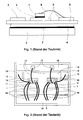
- FIG. 1 the prior art is shown by way of example using a power semiconductor module.
- FIG. 1 the basic structure of a power semiconductor module in cross section and common connection techniques are shown.
- a power semiconductor component (1) is shown, the first copper surface (2) of the DCB substrate facing it and structured therein, the electrically insulating ceramic (3), the second copper surface (4) of the base plate or a heat sink facing the DCB substrate, the base plate or the heat sink (5), the solder connection (6) between the power semiconductor component (1) and the first copper surface (2), the intermediate layer (7) between the second copper surface (4) and the base plate or heat sink (5) and a wire bond connection (8) between the power semiconductor component and the copper surface (2) of the DCB substrate.
- the intermediate layer (7) is either a cohesive solder connection or a flush, heat-conducting layer.
- the rear side contact of the power semiconductor component (on the side facing the substrate), for example the collector in the case of an IGBT as a power semiconductor component (1), with the first copper surface (2) can be realized by means of soldering (6).
- the front connections of the power semiconductor component, for example the gate and the emitter of an IGBT, are preferably connected by means of wire bond connections (8) to one or more connection regions of the first copper surface (2) of the DCB substrate, some of which are insulated from one another.
- the current to be switched with the aid of the power semiconductor component flows through both the large-area solder connection (6) on the back of the power semiconductor component and the wire bond connections of the emitter (8) on the front of the power semiconductor component.
- Even a partial destruction of one of the two connection technologies inevitably leads to a loss of current carrying capacity and consequently to its failure.
- the failure is often not caused by electrical processes, but by other processes such as mechanical stress or changes in material properties as a result of thermal alternating loads.
- FIG. 2 shows an example of a possible structuring of a DCB substrate (9) according to the prior art with the required wire bond connections and two power semiconductor components (1) connected in parallel on a common conductor surface.
- the connections of the power semiconductor components on the side facing away from the substrate are made via contact areas on its surface. These are also known as bond pads, which have different functions. On the one hand, they carry the main current and represent the reference node for the drive circuit. In the case of an IGBT, these are referred to as the emitter bond pad (10). On the other hand, they serve to control the power semiconductor component, referred to as a gate pad (11), for example in the case of an IGBT.
- the connections to the insulated copper surfaces (18) of the DCB substrate are realized by means of wire bond connections (12, 13, 14).
- the bond wires also have different functions.
- the bonding wires required to conduct the main current are referred to as emitter bonding wires (14), the bonding wires required for control as the gate bonding wire (12), and the connection to the reference node as the auxiliary emitter bonding wire (13).
- the auxiliary emitter bond wire (13) can, for example, be used as an extension of an emitter bond wire (14), the auxiliary emitter bond wire (13) having the special feature compared to an emitter bond wire (14) that the main current does not flow through it. This minimizes negative feedback effects in the control circuit due to the current flow in the main circuit.
- the gate bond wires (12) connect the gate bond pads (11) to the gate resistors (17) which are arranged on the gate busbar (18).
- the gate resistors (17) can also be integrated into the power semiconductor component, in which case the gate bond pads (11) are connected directly to the gate busbar (18).
- the detachment of an emitter bond wire (14) causes an interruption of the current flow over the detached bond wire. As a result, the current is divided among the remaining emitter bond wires. This leads to an increasing load and increased probability of failure of the previously intact emitter bond wires (14). As a result, further emitter bond wires (14) separate until there is no longer any connection from the emitter busbar (16) to the emitter bond pads (10) of the semiconductor component.
- the object of the present invention is to present a circuit arrangement and an associated method for the contact failure of electrically conductive connections, in particular wire bond connections, a contact surface of a semiconductor component or a group of electrically conductively connected contact surfaces of a semiconductor component to a further contact surface outside the semiconductor component, for example on the Detect substrate, which results from the partial or complete interruption of this electrically conductive connection, during operation.
- the basic inventive idea lies in a circuit arrangement consisting of at least one power semiconductor component and at least two electrically separate contact areas with the same functionality and / or electrically separate groups of contact areas with the same functionality.
- Each power semiconductor component has at least one such contact area.
- a group of contact areas is to be understood to mean a plurality of contact areas which are electrically conductively connected to one another and are arranged on the same power semiconductor component.
- the circuit arrangement has at least one star point. Each contact area and / or each electrically separated group of contact areas is connected to this star point via at least one active and / or passive component.
- the circuit arrangement also has a contact area outside the power semiconductor components, for example on the substrate, which is connected to the contact areas on the power semiconductor components, for example the emitter busbar.
- the method for monitoring an interruption of a connection between a contact area or a group of contact areas on power semiconductor components and a further contact area outside the semiconductor component is based on the detection of a potential difference between the star point or star points and the contact area outside the semiconductor component.
- the procedure for monitoring an above Circuit arrangement is carried out, for example, by means of a monitoring circuit consisting, inter alia, of from comparators, the signal obtained being used to detect the failure of one or a plurality of electrically conductive connections to a power semiconductor component.
- the circuit arrangement for monitoring the emitter connection is only active when the associated power semiconductor component is switched on.
- the circuit arrangement for monitoring the sensor connection is only active when the associated power semiconductor component is switched off.
- 3 to 8 show the inventive solution based on a power semiconductor module comparable to that of FIGS. 1 and 2.
- the groups of contact areas of claim 1 correspond to the emitter bond pads of each of the individual IGBT power semiconductor components.
- the emitter busbar corresponds to the further contact area outside the semiconductor component.
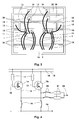
- FIG. 3 shows a circuit arrangement which has been changed according to the invention compared to the prior art according to FIG. 2.
- a further copper-clad area (22) was arranged on the DCB substrate (9).
- Each IGBT is connected to this further copper-clad region (22) by means of an additional emitter bond wire (20) and via a resistor (21).
- These resistors (21) are arranged on the copper surface (22) insulated from the other copper surfaces.
- the copper surface (22) thus represents the star point of a star connection and is connected to an evaluation circuit.
- FIG. 4 shows the electrical network of the inventive circuit arrangement according to FIG. 3 without contact failure of a wire bond connection. Due to the low-resistance connection of the emitters of the IGBTs to the star point, in the static case, i.e. in the period in which the IGBT does not change its switching state, there is no significant potential difference between the emitter busbar (16), the auxiliary emitter connection (19) and the star point of the resistor network (22).
- FIG. 5 shows the electrical network of the inventive circuit arrangement according to FIG. 3 with contact failure of all emitter bond wires of an IGBT. There is therefore no direct connection from the emitter bond pads (10) of this IGBT (1a) to the emitter busbar (16).
- the additional emitter bond wire (20) of this IGBT (1a) via the resistor network, formed from the resistors (21) on the insulated copper surface (22), the additional emitter bond wire (20) of the other IGBT (1b) and its emitter bond wires (14) there is a conductive connection to the emitter busbar (16).
- the emitter of the IGBT (1a), the bond wires of which have become loose experiences negative current feedback via the resistor network of the resistors (21) on the insulated copper surface (22).
- This negative feedback limits the current through the faulty IGBT on the one hand, but also leads to voltage drops across the resistors (21).
- Detection can now be carried out by evaluating the potential difference between the star point (22) and the emitter busbar (16) or the auxiliary emitter connection (19).
- FIG. 6 shows the current and voltage profiles in the network according to FIG. 4 for an on and off cycle of an IGBT.
- the time profiles of the current through the two IGBTs (23), the voltage across the IGBTs (24), and the voltage are shown at the gate of the IGBTs (25) and the voltage at the star point (26).
- the load current (23) increases from zero to about 20A until the IGBTs are switched off. Apart from short pulses during the switching edges (40, 41), the voltage (26) at the star point (22) is very low.
- FIG. 7 shows the current and voltage profiles in the network according to FIG. 5 for an on and off cycle of an IGBT.
- the different profile of the voltage (26) at the star point can be seen during the entire time interval shown.
- the voltage when switched on rises to values of 900mV (42).
- a very clear increase in the voltage at the star point (26) can also be seen during the switch-off delay time (43).
- the star connection can be formed with diodes. Then the signal at the star point is independent of the number of components connected in parallel. In this case, it would be advantageous to detect a current flow from the star point to the evaluation circuit.
- FIG. 8 shows the electrical network of the inventive circuit arrangement for four power components in two groups, a plurality, here two, star circuits being designed for four power components (1a, 1b, 1c, 1d).
- the decoupling of the The signal can occur on the one hand analogously to FIG. 5 between points A and C or B and C. With a symmetrical structure, it is also advantageous to detect and evaluate the signal between points A and B.
- the previously mentioned configuration of the inventive circuit arrangement and the inventive method have the advantages that the method does not require any changes to the power semiconductor components, but only minor changes to the construction and connection technology, and a relatively simple evaluation circuit, which, for example, is a supplementary component of the control and monitoring circuit of the Power semiconductor module is.
- State-of-the-art power semiconductor components such as power bipolar transistors, IGBTs, MOS power transistors and thyristors, are predominantly cellular.
- Cellular structure is understood to mean that doping regions or substructures each having the same electrical function are formed at least twice as spatially separate arrangements within the power component.
- bipolar transistor these can be, for example, emitter doping regions, which are arranged multiple times in the base doping region as strips, squares, hexagons, etc.
- the entire MOS structure is formed multiple times within the substrate area.
- the main and control electrodes of the cellular elements are connected to one another by means of electrically conductive connections.
- electrically conductive connections In the case of an IGBT, for example, all emitter / bulk areas, collector areas and gates are connected by a respective metallization layer on the IGBT. If this is not the case, the connection is made using bond wires.
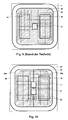
- FIG. 9 shows a top view of a power semiconductor component (IGBT) (1) with a cellular structure according to the prior art.
- the emitter metallization region (28), the IGBT cells (29), the emitter bond pads (10) and the gate bond pad (11) are shown schematically.
- FIG. 10 shows the circuit arrangement according to the invention on the basis of an IGBT power semiconductor component which has been modified compared to the prior art.
- the contact areas of claim 1 correspond to the two emitter bond pads of this IGBT.
- An optional additional contact area on the IGBT corresponds to the star point that is connected to the evaluation circuit.
- the emitter bond pads are connected to the emitter bus bar as a further contact area outside the semiconductor component.
- the shape of the emitter metallization region (28a, 28b) of the IGBT (27) is different from that of the prior art.
- the emitter metallization region is divided into two electrically separate subregions of the emitter metallization (28a, 28b). A division into more than two sub-areas is also possible in a corresponding manner. Only a certain part of the IGBT cells (29) is connected to each sub-area of the emitter metallization (28a, 28b).
- the loss of contact of each electrically separated emitter bond pad can be detected with an arrangement according to FIG. 3.
- the active or passive electronic components of the starter circuit are integrated into the power semiconductor component.
- resistors (30) or diodes can be implemented using doped polysilicon regions.
- Each sub-area of the emitter metallization (28a, 28b) is now connected via an integrated active or passive electronic component (30) to an additional further contact area (31) on the IGBT, which is electrically separated from the other metallization areas of the IGBT.
- the further contact surface (31) is now connected to the evaluation circuit.
- the lifting of the bond wires from an emitter bond pad leads, analogously to FIG. 5, to voltage drops across the integrated resistors (30) in the IGBT.
- the detection can again take place, for example, by evaluating the potential difference between the further contact surface (31) and the emitter busbar (16) or the auxiliary emitter connection (19).
- the correct function of the additional emitter bond wires (20) and the auxiliary emitter bond wire (13) can be determined here by determining the resistance value between points A and C using a corresponding measuring circuit (33, 34).
- FIG. 12 shows an inventive circuit arrangement for four power semiconductor components, for example for IGBTs, with two starter circuits, with which the presence of a conductive connection from the star point (22) of the star circuits to the contact surfaces of the power semiconductor components and to the evaluation circuit can also be monitored.
- VG here denotes the gate drive signal from the driver.
- the measuring bridge is formed by the two resistors at point K (32a, 32b) and the two groups of resistors (21) connected in parallel on the emitters of the IGBTs.
- An electrical signal e.g. a voltage, applied.
- Both the failure of the emitter bond wires (14) or the additional emitter bond wires (20) and the connection between the star point (22) and the evaluation circuit lead to a loss of the balance of the bridge, which can be detected as an electrical signal between points A and B, for example can.
- the loss of the auxiliary emitter bond wire (13) can also be monitored if it is led out separately as in FIG. 11.
- FIG. 13 shows the structure of a circuit arrangement (100) for detecting the failure of electrical connections according to FIG. 12.
- the inputs of the circuit arrangement are designated in accordance with the contact points in FIG. 12.
- the circuit arrangement (100) consists of an error processing unit (110), an error memory (120), an input interface (130) with a reset option, a resistor network (160) and a control unit (140) for controlling a current source (CS) and a plurality of comparators (150).
- the circuit arrangement has three error signal outputs (W1, W2, W3), a voltage supply (VD), an externally connected capacitor (CTCS) and inputs for the gate control voltage (VG), the contact point (C) of the emitter busbar and the contact points (A, B) to the sense wires (20).
- the detection method of failure of an emitter or a sense connection is described below.
- two of the four comparators are connected to contact points (A) and (B), the connection of the second comparator being mirror-symmetrical to the first.
- the third comparator is connected to contact points (A) and (C), and the fourth to contact points (B) and (C). This makes it possible to monitor each of the above connections.
- control unit (140) Monitoring an emitter connection only makes sense if the corresponding IGBT is in the conductive state, this is guaranteed by the control unit (140). It only switches monitoring after the IGBT has been switched on.
- the control variable required for this is formed by the gate control voltage which is present at the input (VG).
- the monitoring of a sense connection only makes sense when an IGBT is in a non-conductive state.
- the current source (CS) is monitored by the control unit (140). switched on. Connecting them to the resistors (160) of the circuit arrangement (100) and the resistors (21, Fig. 12) results in a Wheatstone bridge circuit.
- the output signal of this Wheatson bridge is zero as long as there is no error, it deviates from zero if there is a break in the contact of the sensor connection (20).
- the monitoring of the sense connection is not carried out after each switch-off.
- the number of switching periods after which the sensor connection is checked is adjustable.
- the capacitor (CTCS) is used to set the pulse width in which the current source (CS) is active. Alternatively, the pulse width can also be fixed. Special error codes can be assigned to the various possible errors via several, here three, error outputs (W1, W2, W3).
- FIG. 14 shows a diagram of detection of detachment of the emitter bond wire.
- the error signal is reset to LOW (201).
- Monitoring begins a defined period of time after the IGBT is switched on, for which purpose the gate control voltage (VG) is evaluated.
- the break in an emitter connection (202) is detected and indicated by raising all levels of the output signals (W1, W2, W3) from LOW to HIGH. This error is thus encoded as "111".
- FIG. 15 shows a diagram of detection of detachment of a sense wire. Monitoring begins after a set number of switching periods, here 240 (P240). After switching off, the current source (CS) is activated, see the corresponding voltage curve (VCTCS). An interrupted sense connection is detected as an example and displayed by the change in the output signal (W1) from LOW to HIGH. This error is thus coded as "100".
Landscapes
- Physics & Mathematics (AREA)
- General Physics & Mathematics (AREA)
- Engineering & Computer Science (AREA)
- Microelectronics & Electronic Packaging (AREA)
- Computer Hardware Design (AREA)
- General Engineering & Computer Science (AREA)
- Power Conversion In General (AREA)
- Crystals, And After-Treatments Of Crystals (AREA)
- Semiconductor Integrated Circuits (AREA)
- Internal Circuitry In Semiconductor Integrated Circuit Devices (AREA)
Abstract
Description
- Die Erfindung beschreibt eine Schaltungsanordnung sowie ein dazugehöriges Verfahren zur Überwachung des Kontakts von Drahtbond- oder anderer elektrisch leitender Verbindungen mit Leistungshalbleiterbauelementen, insbesondere bei IGBT- und MOSFET-Leistungshalbleiterschaltern, nach den Merkmalen der Ansprüche 1 und 2.
- Nach dem Stand der Technik sind beispielhaft Drahtbondverbindungen, Lotverbindungen, auch Lotbälle (solder balls) als elektrisch leitende Verbindungen zwischen Substraten und Leistungshalbleiterbauelemente bekannt. Sie gewährleisten die elektrische Verbindung zwischen einem Leistungshalbleiterbauelement und einem Substrat, z.B. einer nach dem direct-copper-bonding hergestellten meist beidseitig kupferkaschierten Keramik (kurz: DCB-Substrat), innerhalb eines Leistungshalbleiter-Moduls, bzw. den Anschluss- Pins (kurz: leadframe) eines diskreten Gehäuses.
- In den Fig. 1 und 2 wird der Stand der Technik beispielhaft anhand eines Leistungshalbleitermoduls dargestellt. In Fig. 1 sind der prinzipielle Aufbau eines Leistungshalbleitermoduls im Querschnitt sowie gängige Verbindungstechniken gezeigt. Dargestellt ist ein Leistungshalbleiterbauelement (1), die diesem zugewandte und in sich strukturierte erste Kupferfläche (2) des DCB- Substrats, die elektrisch isolierende Keramik (3), die einer Grundplatte oder einem Kühlkörper zugewandte zweite Kupferfläche (4) des DCB- Substrats, die Bodenplatte bzw. der Kühlkörper (5), die Lotverbindung (6) zwischen Leistungshalbleiterbauelement (1) und erster Kupferfläche (2), die Zwischenschicht (7) zwischen zweiter Kupferfläche (4) und Grundplatte oder Kühlkörper (5) und eine Drahtbondverbindung (8) zwischen dem Leistungshalbleiterbauelement und der Kupferfläche (2) des DCB- Substrats. Hierbei ist die Zwischenschicht (7) entweder eine stoffschlüssige Lotverbindung oder eine stoffbündige, wärmeleitende, Schicht. Der Rückseitenkontakt des Leistungshalbleiterbauelements (auf der dem Substrat zugewandten Seite), beispielhaft der Kollektor im Falle eines IGBT als Leistungshalbleiterbauelement (1), mit der ersten Kupferfläche (2), kann mittels einer Lötung (6) realisiert werden. Die vorderseitigen Anschlüsse des Leistungshalbleiterbauelements, beispielhaft das Gate und der Emitter eines IGBT, werden vorzugsweise mittels Drahtbondverbindungen (8) mit jeweils einem oder mehreren zum Teil voneinander isolierten Anschlussgebieten der ersten Kupferfläche (2) des DCB- Substrats verbunden. Der mit Hilfe des Leistungshalbleiterbauelements zu schaltende Strom durchfließt sowohl die großflächige Lotverbindung (6) an der Rückseite des Leistungshalbleiterbauelements, als auch die Drahtbondverbindungen des Emitters (8) an der Vorderseite des Leistungshalbleiterbauelements. Eine auch nur teilweise Zerstörung einer der beiden Verbindungstechniken führt zwangsläufig zum Verlust der Stromtragfähigkeit und folglich zu dessen Ausfall. Der Ausfall ist hierbei häufig nicht durch elektrische Vorgänge verursacht, sondern durch weitere Vorgänge wie beispielhaft mechanische Beanspruchung oder Veränderungen der Werkstoffeigenschaften in Folge thermischer Wechselbelastungen.
- Fig. 2 zeigt beispielhaft eine mögliche Strukturierung eines DCB- Substrats (9) nach dem Stand der Technik mit den erforderlichen Drahtbondverbindungen und zwei parallel geschalteten Leistungshalbleiterbauelementen (1) auf einer gemeinsamen Leiterfläche. Die Anschlüsse der Leistungshalbleiterbauelemente auf der dem Substrat abgewandten Seite erfolgt über Kontaktflächen auf dessen Oberfläche. Diese werden auch als Bondpads bezeichnet, die unterschiedliche Funktion besitzen. Zum einen führen sie den Hauptstrom und stellen den Bezugsknoten für die Ansteuerschaltung dar. Im Falle eines IGBT werden diese als Emitterbondpad (10) bezeichnet. Zum anderen dienen sie der Steuerung des Leistungshalbleiterbauelements, beispielhaft im Falle eines IGBT als Gatepad (11) bezeichnet. Die Verbindungen zu den isolierten Kupferflächen (18) des DCB- Substrats werden mittels Drahtbondverbindungen (12, 13, 14) realisiert. Die Bonddrähte besitzen dabei ebenfalls unterschiedliche Funktionen. Die zum Führen des Hauptstromes notwendigen Bonddrähte werden als Emitterbonddrähte (14) bezeichnet, die zur Ansteuerung notwendigen Bonddrähte als Gatebonddraht (12), die Verbindung zum Bezugsknoten als Hilfsemitterbonddraht (13). Der Hilfsemitterbonddraht (13) kann beispielhaft als Verlängerung eines Emitterbonddrahtes (14) ausgebildet, wobei der Hilfsemitterbonddraht (13) gegenüber einem Emitterbonddraht (14) die Besonderheit besitzt, nicht vom Hauptstrom durchflossen zu werden. Damit werden Gegenkoppeleffekte im Ansteuerstromkreis infolge des Stromflusses im Hauptstromkreis minimiert. Bei Parallelschaltung mehrerer IGBTs ist es auch üblich das Hilfsemitterpotential an der Emittersammelschiene (16) abzugreifen und auf den Hilfsemitterbonddraht zu verzichten.
- Die Gatebonddrähte (12) verbinden die Gatebondpads (11) mit den Gatevorwiderständen (17), die auf der Gatesammelschiene (18) angeordnet sind. Nach dem Stand der Technik können die Gatewiderstände (17) auch in das Leistungshalbleiterbauelement integriert werden, dann werden die Gatebondpads (11) direkt mit der Gatesammelschiene (18) verbunden.
- Das Ablösen eines Emitterbonddrahtes (14) bewirkt eine Unterbrechung des Stromflusses über den abgelösten Bonddraht. Infolgedessen teilt sich der Strom auf die übrigen Emitterbonddrähte auf. Das führt zu einer steigenden Belastung und erhöhten Ausfallwahrscheinlichkeit der bisher intakten Emitterbonddrähte (14). In Folge lösen sich weitere Emitterbonddrähte (14) ab, bis keinerlei Verbindung von der Emittersammelschiene (16) zu den Emitterbondpads (10) des Halbleiterbauelements mehr besteht.
- In Leistungshalbleitermodulen höherer Leistung sind in der Regel mehrere Leistungshalbleiterbauelemente parallel geschaltet. Im Falle des Ausfalls aller Emitterbonddrähte eines Chips kommt es dann in der Regel zum sofortigen Ausfall des Moduls. Falls das Modul nicht sofort ausfällt erhöht sich die Belastung der noch intakten Leistungshalbleiterbauelemente, was wiederum deren Lebensdauer vermindert. In weiterer Folge lösen sich von weiteren Leistungshalbleiterbauelementen die Bonddrähte ab, bis es zur Zerstörung aller Leistungshalbleiterbauelementen infolge elektrischer oder thermischer Überlastung kommt.
- Nach dem Stand der Technik sind Ausfallindikatoren für Leistungsmodule zu Diagnosezwecken und zur Ausfallfrüherkennung bekannt. So bewirkt eine sich lösende Chiplötung wie auch sich ablösende Bonddrähte eine Erhöhung der Flussspannung der Leistungshalbleiter im eingeschalteten Zustand bzw. eine Zunahme des thermischen Widerstandes. Diese Größen sind allerdings im Betrieb nicht zugänglich.
- Auch sind beispielhaft aus der EP 0 752 593 A2 Verfahren bekannt, die eine Wechselspannung einer bestimmten Frequenz über eine Drahtbondverbindung leiten und aus einer Messung und Analyse der entstehenden Oberwellen auf defekte Bondverbindungen schließen. Diese Verfahren sind allerdings bisher nur als Sondermessungen außerhalb des Betriebes möglich.
- Weiterhin sind Vorrichtungen zur Detektion des Bonddrahtabhebens auf der Grundlage einer mechanischen Auswertung bekannt. Dabei wird die Haftung der Bondverbindungen über Federkräfte gemessen. Eine Zuverlässigkeitserhöhung lässt sich allerdings nur mit hohem technischen Aufwand, hohen Kosten und dafür benötigtem Volumen erreichen. Auch dieses Verfahren ist, wie alle bisher genannten, nur als Laboraufbau bekannt.
- Die vorliegende Erfindung hat die Aufgabe eine Schaltungsanordnung sowie ein zugehöriges Verfahren vorzustellen, um den Kontaktausfall von elektrisch leitenden Verbindungen, speziell Drahtbondverbindungen, einer Kontaktfläche eines Halbleiterbauelements oder einer Gruppe von elektrisch leitend verbundenen Kontaktflächen eines Halbleiterbauelements zu einer weiteren Kontaktfläche außerhalb des Halbleiterbauelements, beispielhaft auf dem Substrat, der durch die teilweise oder vollständige Unterbrechung dieser elektrisch leitenden Verbindung entsteht, während des Betriebs zu detektieren.
- Diese Aufgabe wird gelöst durch die Maßnahmen der Ansprüche 1 und 2. Weitere vorteilhafte Ausgestaltungen sind in den Unteransprüchen genannt.
- Der grundlegende erfinderische Gedanke liegt in einer Schaltungsanordnung bestehend aus mindestens einem Leistungshalbleiterbauelement und mindestens zwei voneinander elektrisch getrennten Kontaktflächen gleicher Funktionalität und / oder elektrisch getrennten Gruppen von Kontaktflächen gleicher Funktionalität. Jedes Leistungshalbleiterbauelement weist mindestens eine derartige Kontaktfläche auf. Unter einer Gruppe von Kontaktflächen soll eine Mehrzahl von Kontaktflächen verstanden werden, die direkt miteinander elektrisch leitend verbunden sind und auf dem gleichen Leistungshalbleiterbauelement angeordnet sind. Weiterhin weist die Schaltungsanordnung mindestens einen Sternpunkt auf. Jede Kontaktfläche und / oder jede elektrisch getrennte Gruppe von Kontaktflächen ist über mindestens ein aktives und / oder passives Bauelement mit diesem Sternpunkt verbunden.
- Weiterhin weist die Schaltungsanordnung noch eine Kontaktfläche außerhalb der Leistungshalbleiterbauelemente, beispielhaft auf dem Substrat auf, die mit den Kontaktflächen auf den Leistungshalbleiterbauelementen verbunden ist, dies kann beispielhaft die Emittersammelschiene sein.
- Das Verfahren zur Überwachung einer Unterbrechung einer Verbindung zwischen einer Kontaktfläche oder einer Gruppe von Kontaktflächen auf Leistungshalbleiterbauelementen und einer weiteren Kontaktfläche außerhalb des Halbleiterbauelements basiert auf der Detektion einer Potentialdifferenz zwischen dem oder den Sternpunkten und der Kontaktfläche außerhalb des Halbleiterbauelements.
- Das Verfahren zur Überwachung einer o.g. Schaltungsanordnung erfolgt beispielhaft mittels einer Überwachungsschaltung bestehend u.a. aus Komparatoren wobei das gewonnene Signal zur Detektion des Ausfalls eines oder einer Mehrzahl elektrisch leitender Verbindungen zu einem Leistungshalbleiterbauelement verwendet wird. Hierbei ist die Schaltungsanordnung zur Überwachung der Emitterverbindung nur dann aktiv, wenn das zugeordnete Leistungshalbleiterbauelement eingeschaltet ist. Ebenso, oder alternativ ist die Schaltungsanordnung zur Überwachung der Senseverbindung nur dann aktiv, wenn das zugeordnete Leistungshalbleiterbauelement ausgeschaltet ist.
- Spezielle Ausgestaltungen der erfinderischen Lösungen werden an Hand der Fig. 3 bis 15 erläutert.
- Fig. 3
- zeigt eine gegenüber dem Stand der Technik nach Fig. 2 erfinderisch veränderte Schaltungsanordnung.
- Fig. 4
- zeigt das elektrische Netzwerk der erfinderischen Schaltungsanordnung nach Fig. 3 ohne Kontaktausfall.
- Fig. 5
- zeigt das elektrische Netzwerk der erfinderischen Schaltungsanordnung nach Fig. 3 mit Kontaktausfall.
- Fig. 6
- zeigt für einen Ein- und Ausschaltzyklus eines IGBT die Strom- und Spannungsverläufe im Netzwerk nach Fig. 4.
- Fig. 7
- zeigt für einen Ein- und Ausschaltzyklus eines IGBT die Strom- und Spannungsverläufe im Netzwerk nach Fig. 5.
- Fig. 8
- zeigt das elektrische Netzwerk der erfinderische Schaltungsanordnung für vier Leistungshalbleiterbauelemente in zwei Gruppen.
- Fig. 9
- zeigt ein Leistungshalbleiterbauelement (IGBT) mit zellulärem Aufbau nach dem Stand der Technik.
- Fig. 10
- zeigt eine erfinderische Schaltungsanordnung als Teil eines Leistungshalbleiterbauelement.
- Fig. 11
- zeigt eine erfinderische Schaltungsanordnung wobei auch zusätzliche Verbindungen zum Sternpunkt überwacht werden.
- Fig. 12
- zeigt eine erfinderische Schaltungsanordnung für vier Leistungshalbleiterbauelemente in zwei Gruppen.
- Fig. 13
- zeigt den Aufbau einer Schaltungsanordnung zur Detektion des Ausfalls elektrischer Verbindungen gemäß Fig 12.
- Fig. 14
- zeigt ein Diagramm der Detektion einer Ablösung des Emitterbondrahtes.
- Fig. 15
- zeigt ein Diagramm der Detektion einer Ablösung eines Sensedrahtes.
- Fig. 3 bis 8 zeigen die erfinderische Lösung anhand eines Leistungshalbleitermoduls vergleichbar denjenigen aus Fig. 1 und 2. Hierbei entsprechen die Gruppen von Kontaktflächen des Anspruchs 1 den Emitterbondpads jedes der einzelnen IGBT Leistungshalbleiterbauelemente. Die Emittersammelschiene entspricht der weiteren Kontaktfläche außerhalb des Halbleiterbauelements.
- Fig. 3 zeigt eine gegenüber dem Stand der Technik nach Fig. 2 erfinderisch veränderte Schaltungsanordnung. Hierzu wurde ein weiterer kupferkaschierter Bereich (22) auf dem DCB-Substrat (9) angeordnet. Jeder IGBT ist mittels eines zusätzlichen Emitterbonddrahtes (20) und über einen Widerstand (21) mit diesem weiteren kupferkaschierten Bereich (22) verbunden. Diese Widerstände (21) sind dabei auf der von den anderen Kupferflächen isolierten Kupferfläche (22) angeordnet. Die Kupferfläche (22) stellt somit den Stempunkt einer Sternschaltung dar und wird mit einer Auswerteschaltung verbunden.
- Fig. 4 zeigt das elektrische Netzwerk der erfinderischen Schaltungsanordnung nach Fig. 3 ohne Kontaktausfall einer Drahtbondverbindung. Durch die niederohmige Verbindung der Emitter der IGBTs mit dem Sternpunkt besteht im statischen Fall, d.h. in dem Zeitraum in dem der IGBT seinen Schaltzustand nicht ändert, kein signifikanter Potentialunterschied zwischen der Emittersammelschiene (16), dem Hilfsemitteranschluss (19) und dem Sternpunkt des Widerstandsnetzwerks (22).
- Fig. 5 zeigt das elektrische Netzwerk der erfinderischen Schaltungsanordnung nach Fig. 3 mit Kontaktausfall aller Emitterbonddrähte eines IGBTs. Damit besteht von den Emitterbondpads (10) dieses IGBTs (1a) keine direkte Verbindung zur Emitter-Sammelschiene (16). Ausschließlich über den zusätzlichen Emitterbonddraht (20) dieses IGBTs (1a), über das Widerstandsnetzwerk, gebildet aus den Widerständen (21) auf der isolierten Kupferfläche (22), den zusätzlichen Emitterbonddraht (20) des anderen IGBTs (1b) sowie dessen Emitterbonddrähten (14) besteht eine leitenden Verbindung zur Emittersammelschiene (16). Dadurch erfährt der Emitter des IGBT (1a), dessen Bonddrähte sich gelöst haben, eine Stromgegenkopplung über das Widerstandsnetzwerk der Widerstände (21) auf der isolierten Kupferfläche (22). Diese Gegenkopplung begrenzt einerseits den Strom durch den fehlerbehafteten IGBT, führt aber auch zu Spannungsabfällen über den Widerständen (21).
- Eine Detektion kann nun dadurch erfolgen, dass der Potentialunterschied zwischen dem Sternpunkt (22) und der Emittersammelschiene (16) oder dem Hilfsemitteranschluss (19) ausgewertet wird.
- Fig. 6 zeigt für einen Ein- und Ausschaltzyklus eines IGBT die Strom- und Spannungsverläufe im Netzwerk nach Fig. 4. Dargestellt sind die zeitlichen Verläufe des Stromes durch die beiden IGBTs (23), der Spannung über den IGBTs (24), der Spannung am Gate der IGBTs (25) sowie der Spannung am Sternpunkt (26). Dabei steigt der Laststrom (23) von Null beginnend bis zum Abschalten der IGBTs auf etwa 20A. Abgesehen von kurzen Impulsen während der Schaltflanken (40,41) ist die Spannung (26) am Sternpunkt (22) sehr gering.
- Fig. 7 zeigt für einen Ein- und Ausschaltzyklus eines IGBT die Strom- und Spannungsverläufe im Netzwerk nach Fig. 5. Im Vergleich zu Fig. 6 ist der unterschiedliche Verlauf der Spannung (26) am Sternpunkt während des gesamten dargestellten Zeitintervalls zu erkennen. Beispielsweise steigt die Spannung im eingeschalteten Zustand hier bis auf Werte von 900mV (42). Auch während der Abschaltverzögerungszeit ist ein sehr deutlicher Anstieg der Spannung am Sternpunkt (26) zu erkennen (43).
- Je größer die Anzahl an parallel geschalteten IGBTs ist, desto kleiner und somit schwerer auswertbar wird das elektrische Signal am Sternpunkt (22). Dies kann verbessert werden indem das entnommene Signal einer Integratorschaltung zugeführt wird, was zur Steigerung der Störsicherheit und damit der sicheren Detektion führt.
- Weiterhin kann die Sternschaltung mit Dioden gebildet werden. Dann ist das Signal am Sternpunkt unabhängig von der Anzahl der parallelgeschalteten Bauelemente. In diesem Fall wäre es vorteilhaft einen Stromfluss vom Stempunkt zur Auswerteschaltung zu detektieren.
- Fig. 8 zeigt das elektrische Netzwerk der erfinderische Schaltungsanordnung für vier Leistungsbauelemente in zwei Gruppen, wobei eine Mehrzahl, hier zwei, Stemschaltungen ausgebildet sind für vier Leistungsbauelemente (1a, 1b, 1c, 1d). Die Auskopplung des Signals kann einerseits analog Fig. 5 zwischen den Punkten A und C bzw. B und C erfolgen. Bei symmetrischem Aufbau ist es auch vorteilhaft das Signal zwischen den Punkten A und B zu detektieren und auszuwerten.
- Die bisher genannten Ausgestaltung der erfinderischen Schaltungsanordnung sowie des erfinderischen Verfahrens weisen die Vorteile auf, dass das Verfahren keinerlei Änderungen der Leistungshalbleiterbauelemente, sondern lediglich geringfügiger Änderungen der Aufbau- und Verbindungstechnik bedarf sowie einer relativ einfachen Auswerteschaltung, die beispielsweise ergänzender Bestandteil der Ansteuer- und Überwachungsschaltung des Leistungshalbleitermoduls ist.
- Leistungshalbleiterbauelemente nach dem Stand der Technik, wie beispielsweise Leistungs-Bipolartransistoren, IGBTs, MOS- Leistungstransistoren und Thyristoren sind überwiegend zellulär aufgebaut. Unter zellulärem Aufbau ist dabei zu verstehen, dass Dotiergebiete oder Teilstrukturen mit jeweils gleicher elektrischer Funktion mindestens zweifach als räumlich getrennte Anordnungen innerhalb des Leistungsbauelements ausgebildet werden. Im Falle eines Bipolartransistors können dies beispielsweise Emitterdotiergebiete sein, die als Streifen, Vierecke, Sechsecke etc. mehrfach im Basisdotiergebiet angeordnet sind. Im Falle eines IGBTs wird beispielsweise die gesamte MOS- Struktur mehrfach innerhalb des Substratgebiets ausgebildet.
- Kennzeichnend für alle diese Strukturen ist, dass die Haupt- und Steuerelektroden der zellulären Elemente mittels elektrisch leitfähiger Verbindungen miteinander verbunden werden. Im Falle eines IGBTs sind beispielsweise alle Emitter-/Bulkgebiete, Kollektorgebiete und Gates durch eine jeweilige Metallisierungsschicht auf dem IGBT verbunden. Ist dies nicht der Fall, erfolgt die Verbindung über Bonddrähte.
- Fig. 9 zeigt ein Leistungshalbleiterbauelement (IGBT) (1) mit zellulärem Aufbau nach dem Stand der Technik in Draufsicht. Dargestellt ist schematisch das Emittermetallisierungsgebiet (28), die IGBT- Zellen (29), die Emitterbondpads (10) und das Gatebondpad (11).
- Fig. 10 zeigt die erfinderische Schaltungsanordnung anhand eines gegenüber dem Stand der Technik veränderten IGBT Leistungshalbleiterbauelements. Hierbei entsprechen die Kontaktflächen des Anspruchs 1 den beiden Emitterbondpads dieses IGBTs. Eine optionale zusätzliche Kontaktfläche auf dem IGBT entspricht dem Sternpunkt, der mit der Auswerteschaltung verbunden wird. Die Emitterbondpads werden wie oben beschrieben mit der Emittersammelschiene als weitere Kontaktfläche außerhalb des Halbleiterbauelements verbunden.
- Der IGBT (27) ist gegenüber dem Stand der Technik verändert in der Formgebung des Emittermetallisierungsgebiet (28a, 28b). Das Emittermetallisierungsgebiet ist hierzu in zwei voneinander elektrisch getrennte Teilgebiete der Emittermetallisierung (28a, 28b) aufgeteilt. Eine Aufteilung in mehr als zwei Teilgebiete ist ebenso in entsprechender Weise möglich. An jedes Teilgebiet der Emittermetallisierung (28a, 28b) wird nur ein bestimmter Teil der IGBT-Zellen (29) angeschlossen.
- Bei dieser Ausgestaltung der erfinderischen Schaltungsanordnung kann mit einer Anordnung nach Fig. 3 der Kontaktverlust jedes elektrisch getrennten Emitterbondpads detektiert werden.
- Weitere Vorteile ergeben sich, wenn die aktiven oder passiven elektronischen Bauelemente der Stemschaltung in das Leistungshalbleiterbauelement integriert werden. Beispielsweise sind im Falle eines IGBTs Widerstände (30) oder Dioden mittels dotierten Polysilizium-Gebieten realisierbar. Jedes Teilgebiet der Emittermetallisierung (28a, 28b) wird nun über je ein integriertes aktives oder passives elektronisches Bauelement (30) mit einer zusätzlichen weiteren Kontaktfläche (31) auf dem IGBT verbunden, die von den übrigen Metallisierungsgebieten des IGBT elektrisch getrennt ist. Analog zur Verfahrensweise in Fig. 3 wird nun die weitere Kontaktfläche (31) mit der Auswerteschaltung verbunden. Das Abheben der Bonddrähte von einem Emitterbondpad führt analog zu Fig. 5 zu Spannungsabfällen über den integrierten Widerständen (30) im IGBT. Die Detektion kann beispielsweise wiederum dadurch erfolgen, dass der Potentialunterschied zwischen der weiteren Kontaktfläche (31) und der Emittersammelschiene (16) oder dem Hilfsemitteranschluss (19) ausgewertet wird.
- Fig. 11 zeigt eine weitere erfinderische Anordnung für zwei Leistungshalbleiterbauelemente, beispielhaft für IGBTs. Die korrekte Funktion der zusätzlichen Emitterbonddrähte (20) und des Hilfsemitterbonddrahts (13) kann hierbei ermittelt werden, indem der Widerstandswert zwischen den Punkten A und C mit einer entsprechenden Messschaltung (33, 34) ermittelt wird.
- Fig. 12 zeigt eine erfinderische Schaltungsanordnung für vier Leistungshalbleiterbauelemente, beispielhaft für IGBTs, mit zwei Stemschaltungen, mit der ebenfalls das Vorhandensein einer leitfähigen Verbindung vom Sternpunkt (22) der Sternschaltungen zu den Kontaktflächen der Leistungshalbleiterbauelemente und zur Auswerteschaltung überwacht werden kann. VG bezeichnet hier das Gateansteuersignal vom Treiber.
- Die Detektion ist hier auf sehr einfache Weise möglich, da das Prinzip einer Messbrücke angewandt werden kann. Die Messbrücke wird durch die beiden Widerstände am Punkt K (32a, 32b) und den beiden Gruppen parallelgeschalteter Widerständen (21) an den Emittem der IGBTs gebildet. Zwischen den Punkten K und C wird ein elektrisches Signal, z.B. eine Spannung, angelegt. Sowohl der Ausfall der Emitterbonddrähte (14) bzw. der zusätzlichen Emitter-Bonddrähte (20) sowie der Verbindung zwischen Sternpunkt (22) und Auswerteschaltung führen zu einem Verlust des Gleichgewichts der Brücke, was als elektrisches Signal beispielsweise zwischen der Punkten A und B detektiert werden kann. Analog kann auch der Verlust des Hilfsemitterbonddrahtes (13) überwacht werden, wenn er wie in Fig.11 separat herausgeführt ist.
- Fig. 13 zeigt den Aufbau einer Schaltungsanordnung (100) zur Detektion des Ausfalls elektrischer Verbindungen gemäß Fig 12. Die Eingänge der Schaltungsanordnung sind entsprechend den Kontaktpunkten der Fig. 12 bezeichnet. Die Schaltungsanordnung (100) besteht aus einer Fehlerverarbeitungseinheit (110), einem Fehlerspeicher (120), einem Eingangsinterface (130) mit Resetmöglichkeit, einem Widerstandsnetzwerk (160) und einer Steuereinheit (140) zur Ansteurung einer Stromquelle (CS) sowie einer Mehrzahl von Komparatoren (150). Die Schaltungsanordnung weist drei Fehlersignalausgänge (W1, W2, W3), eine Spannungsversorgung (VD), einen extern beschalteten Kondensator (CTCS) sowie Eingänge für die Gateansteuerspannung (VG), den Kontaktpunkt (C ) der Emittersammelschiene und die Kontaktpunkte (A, B) zur den Sensedrähten (20) auf.
- Das Detektionsverfahren des Ausfalls einer Emitter- oder einer Senseverbindung wird im folgenden beschrieben. Hierzu sind zwei der vier Komparatoren mit den Kontaktpunkten (A) und (B) beschaltet, wobei die Beschaltung des zweiten Komparators spiegelsymmetrisch zum ersten ist. Der dritte Komparator ist mit den Kontaktpunkten (A) und (C ), sowie der vierte mit den Kontaktpunkte (B) und (C ) beschaltet. Somit ist die Überwachung jeder einzelnen der oben genannten Verbindungen möglich.
- Die Überwachung einer Emitterverbindung ist nur sinnvoll, wenn der entsprechende IGBT sich im leitenden Zustand befindet, dies wird durch die Steuereinheit (140) gewährleistet. Sie schaltet die Überwachung erst nach dem Einschaltvorgang des IGBTs. Die hierfür notwendige Steuergröße wird durch die Gatesteuerspannung, die am Eingang (VG) anliegt, gebildet.
- Im Gegensatz hierzu ist die Überwachung einer Senseverbindung nur im nicht leitenden Zustand eines IGBTs sinnvoll, die Information hierüber wird ebenfalls aus dem Eingang (VG) gewonnen. Zur Überwachung wird durch die Steuereinheit (140) die Stromquelle (CS) eingeschaltet. Deren Verbindung mit den Widerständen (160) der Schaltungsanordnung (100) sowie der Widerstände (21, Fig. 12) ergibt eine Wheatstone-Brückenschaltung. Das Ausgangssignal dieser Wheatsonebrücke ist Null solange kein Fehler vorliegt, es weicht von Null ab bei Vorliegen einer Kontaktunterbrechung der Senseverbindung (20). Um die Verlustleistung durch dieses Verfahren gering zu halten wird die Überwachung des Senseverbindungen nicht nach jedem Ausschalten ausgeführt. Die Anzahl der Schaltperioden nach der die Senseverbindung geprüft wird ist einstellbar. Der Kondensator (CTCS) dient zur Einstellung der Pulsweite, in der die Stromquelle (CS) aktiv ist. Die Pulweite kann alternativ auch fest eingestellt sein. Den verschiedenen möglichen Fehlem können über mehrere, hier drei, Fehlerausgänge (W1, W2, W3) spezielle Fehlercodes zugewiesen werden.
- Fig. 14 zeigt ein Diagramm der Detektion einer Ablösung des Emitterbondrahtes. Mit Beginn des Einschaltens des IGBTs wird das Fehlersignal auf LOW zurückgesetzt (201). Die Überwachung beginnt eine definierte Zeitspanne nach dem Einschalten des IGBTs, wozu die Gatesteuerspannung (VG) ausgewertet wird. Die Unterbechung einer Emitterverbindung (202) wird detektiert und angezeigt durch das Anheben aller Pegel der Aussangssignale (W1, W2, W3) von LOW auf HIGH. Dieser Fehler ist somit als "111" codiert.
- Fig. 15 zeigt ein Diagramm der Detektion einer Ablösung eines Sensedrahtes. Die Überwachung beginnt nach einer eingestellten Anzahl, hier 240 (P240), von Schaltperioden. Nach dem Ausschalten wird die Stromquelle (CS) aktiviert, siehe entsprechende Spannungskurve (VCTCS). Eine unterbrochene Senseverbindung wird beispielhaft detektiert und angezeigt durch die Änderung des Ausgangssignal (W1) von LOW auf HIGH. Dieser Fehler ist somit als "100" codiert.
Claims (10)
- Schaltungsanordnung bestehend aus mindestens zwei voneinander elektrisch getrennten Kontaktflächen (10) gleicher Funktionalität oder mindestens zwei voneinander elektrisch getrennten Gruppen von Kontaktflächen (10) gleicher Funktionalität, wobei die Kontaktflächen einer Gruppe elektrisch leitend miteinander verbunden sind, diese Kontaktflächen (10)auf mindestens einem Leistungshalbleiterbauelement (1, 27) angeordnet sind und jede elektrisch getrennte Kontaktfläche oder jede elektrisch getrennte Gruppe von Kontaktflächen über mindestens ein aktives und / oder passives Bauelement (17, 30) mit dem Sternpunkt (18, 31) mindestens einer Sternschaltung verbunden ist und alle elektrisch getrennten Kontaktflächen oder alle elektrisch getrennten Gruppen von Kontaktflächen mit mindestens einer weiteren, außerhalb des /der Leistungshalbleiterbauelements/e angeordneten, Kontaktfläche (16, 19) verbunden sind.
- Verfahren zur Überwachung einer Schaltungsanordnung nach Anspruch 1, wobei die Potentialdifferenz zwischen dem oder den Sternpunkten (18, 31) und der weiteren Kontaktfläche (16, 19) außerhalb des Leistungshalbleiterbauelements überwacht wird und das gewonnene Signal zur Detektion des Ausfalls eines oder einer Mehrzahl elektrisch leitender Verbindungen zu einen Leistungshalbleiterbauelement verwendet wird.
- Schaltungsanordnung nach Anspruch 1, wobei
die Kontaktflächen der Leistungshalbeiterbauelemente mit der Sternschaltung und / oder mit der weiteren Kontaktfläche (16, 19) außerhalb des Leistungshalbleiterbauelements mittels elektrisch leitender Verbindungen (12, 13, 14) verbunden sind. - Schaltungsanordnung nach Anspruch 3, wobei
die elektrisch leitenden Verbindungen (12, 13, 14) Drahtbondverbindungen sind. - Schaltungsanordnung nach Anspruch 1 wobei
das oder die Leistungshalbleiterbauelemente (1) IGBT oder MOSFET Transistoren sind. - Schaltungsanordnung nach Anspruch 1 wobei
das oder die Leistungshalbleiterbauelemente (27) IGBT oder MOSFET Transistor sind mit je mindestens zwei elektrisch voneinander getrennten Kontaktflächen (10) und diese Kontaktflächen internen Gruppen von Zellen (29) zugeordneten sind und diese Kontaktflächen mittels mindestens je einem in das Halbleiterbauelement (27) integrierten aktiven und / oder passiven Bauelement (30) mit einem auf dem Leistungshalbleiterbauelement (27) angeordnetem Stempunkt (31) verbunden sind. - Schaltungsanordnung nach Anspruch 1 wobei
eine Mehrzahl von Sternschaltungen zusammen mit weiteren passiven und / oder aktiven Bauelementen (32) eine Brückenschaltung bilden und das elektrische Signal an der Brückenschaltung das zu überwachende ist. - Verfahren nach Anspruch 2, wobei
die Potentialdifferenz zwischen dem oder den Stempunkten (18, 31) und der weiteren Kontaktfläche (16, 19) außerhalb des Leistungshalbleiterbauelements mittels einer Überwachungsschaltung aus Komparatoren überwacht wird und das gewonnene Signal zur Detektion des Ausfalls eines oder einer Mehrzahl elektrisch leitender Verbindungen zu einem Leistungshalbleiterbauelement verwendet wird, wobei die Schaltungsanordnung zur Überwachung der Emitterverbindung (14) nur nach dem Einschalten des zugeordneten Leistungshalbleiterbauelements aktiv ist und / oder die Schaltungsanordnung zur Überwachung der Senseverbindung (20) nur nach dem Ausschalten des zugeordneten Leistungshalbleiterbauelements nicht aktiv ist - Verfahren nach Anspruch 8, wobei
die Senseverbindungen mittels einer Wheatstone- Brückenschaltung überwacht werden, die durch eine Stromquelle (CS) gespeisten wird, und ein Ausgangssignal dieser Brückenschaltung ungleich Null nach einer Schwellwertbildung ein Fehlersignal darstellt. - Verfahren nach Anspruch 8, wobei
die Überwachung der Senseverbindungen jeweils nur nach einer Mehrzahl von Schaltperioden des Leistungshalbleiterbauelements durchgeführt wird.
Applications Claiming Priority (4)
| Application Number | Priority Date | Filing Date | Title |
|---|---|---|---|
| DE10249712 | 2002-10-25 | ||
| DE10249712A DE10249712B3 (de) | 2002-10-25 | 2002-10-25 | Schaltungsanordnung und Verfahren zur Überwachung von Leistungshalbleiterbauelementen |
| DE10316357 | 2003-04-10 | ||
| DE10316357A DE10316357B4 (de) | 2002-10-25 | 2003-04-10 | Verfahren zur Überwachung von Leistungshalbleiterbauelementen |
Publications (2)
| Publication Number | Publication Date |
|---|---|
| EP1414066A1 true EP1414066A1 (de) | 2004-04-28 |
| EP1414066B1 EP1414066B1 (de) | 2009-07-29 |
Family
ID=32070728
Family Applications (1)
| Application Number | Title | Priority Date | Filing Date |
|---|---|---|---|
| EP03023086A Expired - Lifetime EP1414066B1 (de) | 2002-10-25 | 2003-10-15 | Verfahren zur Überwachung von Leistungshalbleiterbauelementen |
Country Status (5)
| Country | Link |
|---|---|
| EP (1) | EP1414066B1 (de) |
| AT (1) | ATE438199T1 (de) |
| DE (2) | DE10316357B4 (de) |
| DK (1) | DK1414066T3 (de) |
| ES (1) | ES2328124T3 (de) |
Cited By (3)
| Publication number | Priority date | Publication date | Assignee | Title |
|---|---|---|---|---|
| CN102364345A (zh) * | 2010-06-21 | 2012-02-29 | 英飞凌科技股份有限公司 | 具有并联电阻的电路装置 |
| EP2629108A1 (de) * | 2012-02-20 | 2013-08-21 | Tellabs Oy | Anordnung mit Zustandsüberwachung und Verfahren zur Zustandsüberwachung |
| EP3121612A1 (de) * | 2015-07-21 | 2017-01-25 | ABB Technology AG | Ausfallvorhersage von leistungshalbleitermodulen |
Families Citing this family (2)
| Publication number | Priority date | Publication date | Assignee | Title |
|---|---|---|---|---|
| US8853835B2 (en) | 2012-10-05 | 2014-10-07 | Infineon Technologies Ag | Chip arrangements, a chip package and a method for manufacturing a chip arrangement |
| CN113994467B (zh) * | 2019-06-25 | 2025-04-04 | 三菱电机株式会社 | 半导体装置以及电力变换装置 |
Citations (4)
| Publication number | Priority date | Publication date | Assignee | Title |
|---|---|---|---|---|
| EP1028465A2 (de) * | 1999-02-05 | 2000-08-16 | Kabushiki Kaisha Toyoda Jidoshokki Seisakusho | Halbleitermodul |
| DE10005754A1 (de) * | 1999-08-12 | 2001-08-23 | Semikron Elektronik Gmbh | Leistungshalbleiterschaltungsanordnung mit schwingungsgedämpfter Parallelschaltung |
| US20010019169A1 (en) * | 1999-12-23 | 2001-09-06 | Filippo Marino | Electronic device with double-wire bonding, manufacturing method thereof, and method for checking intactness of bonding wires of this electronic device |
| US20020024135A1 (en) * | 2000-08-28 | 2002-02-28 | Mitsubishi Denki Kabushiki Kaisha | Semiconductor device |
-
2003
- 2003-04-10 DE DE10316357A patent/DE10316357B4/de not_active Expired - Fee Related
- 2003-10-15 EP EP03023086A patent/EP1414066B1/de not_active Expired - Lifetime
- 2003-10-15 AT AT03023086T patent/ATE438199T1/de not_active IP Right Cessation
- 2003-10-15 DE DE50311749T patent/DE50311749D1/de not_active Expired - Lifetime
- 2003-10-15 DK DK03023086T patent/DK1414066T3/da active
- 2003-10-15 ES ES03023086T patent/ES2328124T3/es not_active Expired - Lifetime
Patent Citations (4)
| Publication number | Priority date | Publication date | Assignee | Title |
|---|---|---|---|---|
| EP1028465A2 (de) * | 1999-02-05 | 2000-08-16 | Kabushiki Kaisha Toyoda Jidoshokki Seisakusho | Halbleitermodul |
| DE10005754A1 (de) * | 1999-08-12 | 2001-08-23 | Semikron Elektronik Gmbh | Leistungshalbleiterschaltungsanordnung mit schwingungsgedämpfter Parallelschaltung |
| US20010019169A1 (en) * | 1999-12-23 | 2001-09-06 | Filippo Marino | Electronic device with double-wire bonding, manufacturing method thereof, and method for checking intactness of bonding wires of this electronic device |
| US20020024135A1 (en) * | 2000-08-28 | 2002-02-28 | Mitsubishi Denki Kabushiki Kaisha | Semiconductor device |
Cited By (7)
| Publication number | Priority date | Publication date | Assignee | Title |
|---|---|---|---|---|
| CN102364345A (zh) * | 2010-06-21 | 2012-02-29 | 英飞凌科技股份有限公司 | 具有并联电阻的电路装置 |
| CN102364345B (zh) * | 2010-06-21 | 2015-07-01 | 英飞凌科技股份有限公司 | 具有所装配的电路载体的电路装置及相应功率半导体模块 |
| EP2629108A1 (de) * | 2012-02-20 | 2013-08-21 | Tellabs Oy | Anordnung mit Zustandsüberwachung und Verfahren zur Zustandsüberwachung |
| CN103260352A (zh) * | 2012-02-20 | 2013-08-21 | 特拉博斯股份有限公司 | 带有状态监视的组件和用于状态监视的方法 |
| US9105173B2 (en) | 2012-02-20 | 2015-08-11 | Coriant Oy | Assembly with condition monitoring and a method for condition monitoring |
| CN103260352B (zh) * | 2012-02-20 | 2017-08-29 | 特拉博斯股份有限公司 | 带有状态监视的组件和用于状态监视的方法 |
| EP3121612A1 (de) * | 2015-07-21 | 2017-01-25 | ABB Technology AG | Ausfallvorhersage von leistungshalbleitermodulen |
Also Published As
| Publication number | Publication date |
|---|---|
| DK1414066T3 (da) | 2009-10-05 |
| ES2328124T3 (es) | 2009-11-10 |
| DE50311749D1 (de) | 2009-09-10 |
| DE10316357B4 (de) | 2005-02-10 |
| EP1414066B1 (de) | 2009-07-29 |
| DE10316357A1 (de) | 2004-11-04 |
| ATE438199T1 (de) | 2009-08-15 |
Similar Documents
| Publication | Publication Date | Title |
|---|---|---|
| EP3224631A1 (de) | Verfahren zur bestimmung einer alterung von leistungshalbleitermodulen sowie vorrichtung und schaltungsanordnung | |
| EP3608644B1 (de) | Verfahren zum bestimmen eines vorzeichens eines laststroms in einer brückenschaltung mit mindestenes einer leistungshalbleiterschaltung | |
| DE10113967B4 (de) | Leistungsmodule | |
| DE102006060768A1 (de) | Gehäusegruppe für Geräte hoher Leistungsdichte | |
| EP2565608B1 (de) | Halbleiterbauelement in Chipbauweise | |
| DE112009004562T5 (de) | Halbleiterstückverbindungsüberwachungssystem und -verfahren | |
| DE112018002579T5 (de) | Halbleiterbauelement | |
| DE102018131999A1 (de) | Leistungsmodul und leistungwandler | |
| DE102015108412A1 (de) | Integrierter Temperatursensor | |
| EP1414066B1 (de) | Verfahren zur Überwachung von Leistungshalbleiterbauelementen | |
| EP1573917B1 (de) | Halbleiterschaltungsanordnung zum steuern einer hohen spannung oder eines stromes grosser stromst rke | |
| DE102014201781A1 (de) | Anordnung und verfahren zum messen der chiptemperatur in einem leistungshalbleitermodul | |
| DE10211831B4 (de) | Schaltungsanordnung und Verfahren zur Überwachung von Leistungshalbleiterbauelementen | |
| DE10159020C1 (de) | Schaltungsanordnung und Verfahren zur Überwachung von Leistungshalbleiterbauelementen | |
| EP1860447B1 (de) | Prüfschaltungsanordnung und Prüfverfahren zum Prüfen einer Schaltungsstrecke einer Schaltung | |
| DE102004036520B4 (de) | Bauelementanordnung mit einer Auswerteschaltung zur Detektion eines Verschleißes von Anschlussverbindungen und Verfahren zur Detektion eines Verschleißes von Anschlussverbindungen | |
| DE10249712B3 (de) | Schaltungsanordnung und Verfahren zur Überwachung von Leistungshalbleiterbauelementen | |
| DE202016101991U1 (de) | Mit erhöhter Chipausbeute hergestelltes Leistungshalbleitermodul | |
| DE102004028695B3 (de) | Halbleiterbauelement mit einem Bruchsensor | |
| DE112018004107T5 (de) | Strommessvorrichtung | |
| WO2020104281A1 (de) | Leistungselektronikanordnung mit einem temperatursensor | |
| EP1577676A1 (de) | Verfahren und Schaltung zum Schutz von Prüfkontakten bei der Hochstrom-Messung von Halbleiter-Bauelementen | |
| DE112021003076T5 (de) | Halbleitermodul | |
| DE102014117512B4 (de) | Halbleitervorrichtung mit Metallstruktur in einer äussersten Verdrahtungsschicht und Via | |
| DE102024131133A1 (de) | Verfahren zur Diagnose einer Inter-Chip-Verbindung in einem Mikrosystem mit mehreren Chips |
Legal Events
| Date | Code | Title | Description |
|---|---|---|---|
| PUAI | Public reference made under article 153(3) epc to a published international application that has entered the european phase |
Free format text: ORIGINAL CODE: 0009012 |
|
| 17P | Request for examination filed |
Effective date: 20040223 |
|
| AK | Designated contracting states |
Kind code of ref document: A1 Designated state(s): AT BE BG CH CY CZ DE DK EE ES FI FR GB GR HU IE IT LI LU MC NL PT RO SE SI SK TR |
|
| AX | Request for extension of the european patent |
Extension state: AL LT LV MK |
|
| 17Q | First examination report despatched |
Effective date: 20040607 |
|
| AKX | Designation fees paid |
Designated state(s): AT BE BG CH CY CZ DE DK EE ES FI FR GB GR HU IE IT LI LU MC NL PT RO SE SI SK TR |
|
| RAP1 | Party data changed (applicant data changed or rights of an application transferred) |
Owner name: SEMIKRON ELEKTRONIK GMBH & CO. KG |
|
| RIC1 | Information provided on ipc code assigned before grant |
Ipc: G01R 31/27 20060101ALI20090122BHEP Ipc: H01L 23/498 20060101ALI20090122BHEP Ipc: H01L 25/07 20060101AFI20090122BHEP Ipc: H01L 25/16 20060101ALI20090122BHEP Ipc: G01R 31/316 20060101ALI20090122BHEP Ipc: G01R 31/28 20060101ALI20090122BHEP Ipc: G01R 31/04 20060101ALI20090122BHEP Ipc: H01L 23/544 20060101ALI20090122BHEP |
|
| RTI1 | Title (correction) |
Free format text: METHOD FOR MONITORING SEMICONDUCTOR POWER ELEMENTS |
|
| GRAP | Despatch of communication of intention to grant a patent |
Free format text: ORIGINAL CODE: EPIDOSNIGR1 |
|
| GRAS | Grant fee paid |
Free format text: ORIGINAL CODE: EPIDOSNIGR3 |
|
| GRAA | (expected) grant |
Free format text: ORIGINAL CODE: 0009210 |
|
| AK | Designated contracting states |
Kind code of ref document: B1 Designated state(s): AT BE BG CH CY CZ DE DK EE ES FI FR GB GR HU IE IT LI LU MC NL PT RO SE SI SK TR |
|
| REG | Reference to a national code |
Ref country code: GB Ref legal event code: FG4D Free format text: NOT ENGLISH |
|
| REG | Reference to a national code |
Ref country code: CH Ref legal event code: EP |
|
| REG | Reference to a national code |
Ref country code: CH Ref legal event code: NV Representative=s name: BRAUNPAT BRAUN EDER AG |
|
| REG | Reference to a national code |
Ref country code: IE Ref legal event code: FG4D |
|
| REF | Corresponds to: |
Ref document number: 50311749 Country of ref document: DE Date of ref document: 20090910 Kind code of ref document: P |
|
| REG | Reference to a national code |
Ref country code: DK Ref legal event code: T3 |
|
| REG | Reference to a national code |
Ref country code: ES Ref legal event code: FG2A Ref document number: 2328124 Country of ref document: ES Kind code of ref document: T3 |
|
| REG | Reference to a national code |
Ref country code: SE Ref legal event code: TRGR |
|
| REG | Reference to a national code |
Ref country code: SK Ref legal event code: T3 Ref document number: E 6230 Country of ref document: SK |
|
| PG25 | Lapsed in a contracting state [announced via postgrant information from national office to epo] |
Ref country code: FI Free format text: LAPSE BECAUSE OF FAILURE TO SUBMIT A TRANSLATION OF THE DESCRIPTION OR TO PAY THE FEE WITHIN THE PRESCRIBED TIME-LIMIT Effective date: 20090729 |
|
| PG25 | Lapsed in a contracting state [announced via postgrant information from national office to epo] |
Ref country code: SI Free format text: LAPSE BECAUSE OF FAILURE TO SUBMIT A TRANSLATION OF THE DESCRIPTION OR TO PAY THE FEE WITHIN THE PRESCRIBED TIME-LIMIT Effective date: 20090729 |
|
| REG | Reference to a national code |
Ref country code: IE Ref legal event code: FD4D |
|
| PG25 | Lapsed in a contracting state [announced via postgrant information from national office to epo] |
Ref country code: PT Free format text: LAPSE BECAUSE OF FAILURE TO SUBMIT A TRANSLATION OF THE DESCRIPTION OR TO PAY THE FEE WITHIN THE PRESCRIBED TIME-LIMIT Effective date: 20091129 Ref country code: BG Free format text: LAPSE BECAUSE OF FAILURE TO SUBMIT A TRANSLATION OF THE DESCRIPTION OR TO PAY THE FEE WITHIN THE PRESCRIBED TIME-LIMIT Effective date: 20091029 |
|
| BERE | Be: lapsed |
Owner name: SEMIKRON ELEKTRONIK G.M.B.H. & CO. KG Effective date: 20091031 |
|
| PG25 | Lapsed in a contracting state [announced via postgrant information from national office to epo] |
Ref country code: IE Free format text: LAPSE BECAUSE OF FAILURE TO SUBMIT A TRANSLATION OF THE DESCRIPTION OR TO PAY THE FEE WITHIN THE PRESCRIBED TIME-LIMIT Effective date: 20090729 Ref country code: EE Free format text: LAPSE BECAUSE OF FAILURE TO SUBMIT A TRANSLATION OF THE DESCRIPTION OR TO PAY THE FEE WITHIN THE PRESCRIBED TIME-LIMIT Effective date: 20090729 Ref country code: RO Free format text: LAPSE BECAUSE OF FAILURE TO SUBMIT A TRANSLATION OF THE DESCRIPTION OR TO PAY THE FEE WITHIN THE PRESCRIBED TIME-LIMIT Effective date: 20090729 Ref country code: CZ Free format text: LAPSE BECAUSE OF FAILURE TO SUBMIT A TRANSLATION OF THE DESCRIPTION OR TO PAY THE FEE WITHIN THE PRESCRIBED TIME-LIMIT Effective date: 20090729 |
|
| PG25 | Lapsed in a contracting state [announced via postgrant information from national office to epo] |
Ref country code: MC Free format text: LAPSE BECAUSE OF NON-PAYMENT OF DUE FEES Effective date: 20091031 |
|
| PLBE | No opposition filed within time limit |
Free format text: ORIGINAL CODE: 0009261 |
|
| STAA | Information on the status of an ep patent application or granted ep patent |
Free format text: STATUS: NO OPPOSITION FILED WITHIN TIME LIMIT |
|
| 26N | No opposition filed |
Effective date: 20100503 |
|
| PG25 | Lapsed in a contracting state [announced via postgrant information from national office to epo] |
Ref country code: GR Free format text: LAPSE BECAUSE OF FAILURE TO SUBMIT A TRANSLATION OF THE DESCRIPTION OR TO PAY THE FEE WITHIN THE PRESCRIBED TIME-LIMIT Effective date: 20091030 Ref country code: BE Free format text: LAPSE BECAUSE OF NON-PAYMENT OF DUE FEES Effective date: 20091031 |
|
| PG25 | Lapsed in a contracting state [announced via postgrant information from national office to epo] |
Ref country code: AT Free format text: LAPSE BECAUSE OF NON-PAYMENT OF DUE FEES Effective date: 20091015 |
|
| PG25 | Lapsed in a contracting state [announced via postgrant information from national office to epo] |
Ref country code: LU Free format text: LAPSE BECAUSE OF NON-PAYMENT OF DUE FEES Effective date: 20091015 |
|
| PG25 | Lapsed in a contracting state [announced via postgrant information from national office to epo] |
Ref country code: HU Free format text: LAPSE BECAUSE OF FAILURE TO SUBMIT A TRANSLATION OF THE DESCRIPTION OR TO PAY THE FEE WITHIN THE PRESCRIBED TIME-LIMIT Effective date: 20100130 |
|
| PG25 | Lapsed in a contracting state [announced via postgrant information from national office to epo] |
Ref country code: TR Free format text: LAPSE BECAUSE OF FAILURE TO SUBMIT A TRANSLATION OF THE DESCRIPTION OR TO PAY THE FEE WITHIN THE PRESCRIBED TIME-LIMIT Effective date: 20090729 |
|
| PG25 | Lapsed in a contracting state [announced via postgrant information from national office to epo] |
Ref country code: CY Free format text: LAPSE BECAUSE OF FAILURE TO SUBMIT A TRANSLATION OF THE DESCRIPTION OR TO PAY THE FEE WITHIN THE PRESCRIBED TIME-LIMIT Effective date: 20090729 |
|
| PGFP | Annual fee paid to national office [announced via postgrant information from national office to epo] |
Ref country code: FR Payment date: 20120904 Year of fee payment: 10 Ref country code: DK Payment date: 20121005 Year of fee payment: 10 |
|
| PGFP | Annual fee paid to national office [announced via postgrant information from national office to epo] |
Ref country code: DE Payment date: 20121031 Year of fee payment: 10 Ref country code: CH Payment date: 20121030 Year of fee payment: 10 |
|
| PGFP | Annual fee paid to national office [announced via postgrant information from national office to epo] |
Ref country code: GB Payment date: 20121105 Year of fee payment: 10 Ref country code: ES Payment date: 20121019 Year of fee payment: 10 Ref country code: IT Payment date: 20121029 Year of fee payment: 10 Ref country code: SK Payment date: 20121011 Year of fee payment: 10 Ref country code: SE Payment date: 20121024 Year of fee payment: 10 |
|
| PGFP | Annual fee paid to national office [announced via postgrant information from national office to epo] |
Ref country code: NL Payment date: 20121019 Year of fee payment: 10 |
|
| REG | Reference to a national code |
Ref country code: NL Ref legal event code: V1 Effective date: 20140501 |
|
| REG | Reference to a national code |
Ref country code: DK Ref legal event code: EBP Effective date: 20131031 |
|
| REG | Reference to a national code |
Ref country code: CH Ref legal event code: PL |
|
| REG | Reference to a national code |
Ref country code: SE Ref legal event code: EUG |
|
| GBPC | Gb: european patent ceased through non-payment of renewal fee |
Effective date: 20131015 |
|
| REG | Reference to a national code |
Ref country code: SK Ref legal event code: MM4A Ref document number: E 6230 Country of ref document: SK Effective date: 20131015 |
|
| PG25 | Lapsed in a contracting state [announced via postgrant information from national office to epo] |
Ref country code: CH Free format text: LAPSE BECAUSE OF NON-PAYMENT OF DUE FEES Effective date: 20131031 Ref country code: GB Free format text: LAPSE BECAUSE OF NON-PAYMENT OF DUE FEES Effective date: 20131015 Ref country code: LI Free format text: LAPSE BECAUSE OF NON-PAYMENT OF DUE FEES Effective date: 20131031 |
|
| REG | Reference to a national code |
Ref country code: FR Ref legal event code: ST Effective date: 20140630 |
|
| REG | Reference to a national code |
Ref country code: DE Ref legal event code: R119 Ref document number: 50311749 Country of ref document: DE Effective date: 20140501 |
|
| PG25 | Lapsed in a contracting state [announced via postgrant information from national office to epo] |
Ref country code: SK Free format text: LAPSE BECAUSE OF NON-PAYMENT OF DUE FEES Effective date: 20131015 Ref country code: IT Free format text: LAPSE BECAUSE OF NON-PAYMENT OF DUE FEES Effective date: 20131015 Ref country code: SE Free format text: LAPSE BECAUSE OF NON-PAYMENT OF DUE FEES Effective date: 20131016 Ref country code: FR Free format text: LAPSE BECAUSE OF NON-PAYMENT OF DUE FEES Effective date: 20131031 Ref country code: DE Free format text: LAPSE BECAUSE OF NON-PAYMENT OF DUE FEES Effective date: 20140501 Ref country code: NL Free format text: LAPSE BECAUSE OF NON-PAYMENT OF DUE FEES Effective date: 20140501 |
|
| PG25 | Lapsed in a contracting state [announced via postgrant information from national office to epo] |
Ref country code: DK Free format text: LAPSE BECAUSE OF NON-PAYMENT OF DUE FEES Effective date: 20131031 |
|
| REG | Reference to a national code |
Ref country code: ES Ref legal event code: FD2A Effective date: 20150709 |
|
| PG25 | Lapsed in a contracting state [announced via postgrant information from national office to epo] |
Ref country code: ES Free format text: LAPSE BECAUSE OF NON-PAYMENT OF DUE FEES Effective date: 20131016 |