EP1410126B1 - Source de courant differentiel a reduction de tension de mode commun sous retroaction active - Google Patents
Source de courant differentiel a reduction de tension de mode commun sous retroaction active Download PDFInfo
- Publication number
- EP1410126B1 EP1410126B1 EP01275082A EP01275082A EP1410126B1 EP 1410126 B1 EP1410126 B1 EP 1410126B1 EP 01275082 A EP01275082 A EP 01275082A EP 01275082 A EP01275082 A EP 01275082A EP 1410126 B1 EP1410126 B1 EP 1410126B1
- Authority
- EP
- European Patent Office
- Prior art keywords
- current source
- load
- voltage
- voltage controlled
- common mode
- Prior art date
- Legal status (The legal status is an assumption and is not a legal conclusion. Google has not performed a legal analysis and makes no representation as to the accuracy of the status listed.)
- Expired - Lifetime
Links
- 230000009467 reduction Effects 0.000 title claims abstract description 17
- 238000005259 measurement Methods 0.000 description 6
- 230000008901 benefit Effects 0.000 description 5
- 239000003990 capacitor Substances 0.000 description 4
- 230000008859 change Effects 0.000 description 4
- 238000010586 diagram Methods 0.000 description 4
- 238000000034 method Methods 0.000 description 3
- 230000009471 action Effects 0.000 description 2
- 230000000694 effects Effects 0.000 description 2
- 230000006978 adaptation Effects 0.000 description 1
- 230000008878 coupling Effects 0.000 description 1
- 238000010168 coupling process Methods 0.000 description 1
- 238000005859 coupling reaction Methods 0.000 description 1
- 230000005284 excitation Effects 0.000 description 1
- 238000002847 impedance measurement Methods 0.000 description 1
- 238000002955 isolation Methods 0.000 description 1
- 238000012986 modification Methods 0.000 description 1
- 230000004048 modification Effects 0.000 description 1
Images

Classifications
-
- H—ELECTRICITY
- H03—ELECTRONIC CIRCUITRY
- H03F—AMPLIFIERS
- H03F3/00—Amplifiers with only discharge tubes or only semiconductor devices as amplifying elements
- H03F3/45—Differential amplifiers
- H03F3/45071—Differential amplifiers with semiconductor devices only
- H03F3/45076—Differential amplifiers with semiconductor devices only characterised by the way of implementation of the active amplifying circuit in the differential amplifier
- H03F3/45475—Differential amplifiers with semiconductor devices only characterised by the way of implementation of the active amplifying circuit in the differential amplifier using IC blocks as the active amplifying circuit
-
- H—ELECTRICITY
- H03—ELECTRONIC CIRCUITRY
- H03F—AMPLIFIERS
- H03F3/00—Amplifiers with only discharge tubes or only semiconductor devices as amplifying elements
- H03F3/45—Differential amplifiers
- H03F3/45071—Differential amplifiers with semiconductor devices only
- H03F3/45479—Differential amplifiers with semiconductor devices only characterised by the way of common mode signal rejection
- H03F3/45928—Differential amplifiers with semiconductor devices only characterised by the way of common mode signal rejection using IC blocks as the active amplifying circuit
- H03F3/45932—Differential amplifiers with semiconductor devices only characterised by the way of common mode signal rejection using IC blocks as the active amplifying circuit by using feedback means
- H03F3/45937—Measuring at the loading circuit of the differential amplifier
- H03F3/45941—Controlling the input circuit of the differential amplifier
-
- H—ELECTRICITY
- H03—ELECTRONIC CIRCUITRY
- H03F—AMPLIFIERS
- H03F2203/00—Indexing scheme relating to amplifiers with only discharge tubes or only semiconductor devices as amplifying elements covered by H03F3/00
- H03F2203/45—Indexing scheme relating to differential amplifiers
- H03F2203/45138—Two or more differential amplifiers in IC-block form are combined, e.g. measuring amplifiers
-
- H—ELECTRICITY
- H03—ELECTRONIC CIRCUITRY
- H03F—AMPLIFIERS
- H03F2203/00—Indexing scheme relating to amplifiers with only discharge tubes or only semiconductor devices as amplifying elements covered by H03F3/00
- H03F2203/45—Indexing scheme relating to differential amplifiers
- H03F2203/45441—Indexing scheme relating to differential amplifiers the CMCL comprising an integrating circuit
Definitions
- the present invention relates to electrical circuits for providing current through a load impedance, where the current source is differential and provides a symmetrical, high impedance drive to the load.
- This type of current source is particularly useful in instrumentation that makes impedance measurements using low excitation.
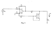
- a modified Howland current source illustrated in FIG. 1, is an example of a current source that will drive a grounded load. It was developed specifically to drive current into a load that has one end tied to the current source ground, ensuring low impedance between the load and ground.
- the Howland current source with its many variations and improvements has been used very successfully in instrumentation, but it does have one drawback.
- the current source output and return have different impedances, creating an unbalanced load. Different impedances at each end of a current source load do not create a problem for the current source in isolation, but in application there is always some stray noise coupling into the load. Most noise couples either capacitively or inductively from the environment into the current source leads. Noise can also couple through the voltage measurement circuits via their power supplies. Much of the noise couples into the load as common-mode current. Differential voltage inputs are used extensively to reject common mode voltage noise but they too are limited.
- One method for balancing the load is to provide a differential current source with a symmetrical, high impedance drive to the load.
- An early example of a differential current drive is the circuit described in NASA Tech Brief #MSC-16475, Winter 1977. This circuit provides differential output with two identical, out of phase outputs, but drives one end of the load from zero source impedance. This effectively introduces a ground at one end of the load and will not eliminate common mode voltage errors.
- a second example of a differential current source is the circuit described in U.S. Pat. No. 5,021,729.
- This differential current source is a practical circuit and achieves the goal of minimizing the effect of common mode voltage on precision measurements as long as the load remains floating. However, if one side of the load is grounded to the current source common there is a significant error in current output.
- the primary object of the present invention is to provide a new current source that operates as a differential -current source when the load is floating and, upon grounding the load, will automatically operate as a grounded load current source with reduced common mode rejection.
- Another objective is to ensure the load current will change only by a small, predictable amount when operation changes from one mode to another, thereby enabling the invention to be used in applications where the measurement wiring is pre-installed and difficult to change or when unintentional grounding occurs during operation.
- Another objective is to create a current source that can be configured for an operation selected from the group consisting of AC operation, DC operation, unipolar operation, bipolar operation, for operation with resistive loads, for operation with reactive loads, and a combination thereof.
- Another objective is that the invention can be easily modified for range selection by switching in sense resistors of different values.
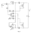
- the present invention is constructed of two, substantially identical, modified Howland current sources driving the load simultaneously but out of phase with each other.
- the current from each half is equal to the full desired current output but they have opposite sign.
- An external voltage source drives one half of the current source and an amplifier is used to create an opposite phase voltage to drive the other half.
- the inverting amplifier can optionally be omitted if the second half of the current source is configured for inverting operation.
- the invention requires active feedback, to center its operation about ground. This prevents the current source output amplifiers from floating to one power supply rail or the other (e.g., active feedback comprising a means to center the operating voltage between power supply rails).
- the circuits used to center operation also act to reduce DC current if the current source is configured for AC operation.
- the near perfect symmetry of the circuit according to the present invention allows one half to operate essentially alone if the other is grounded. Any impedance between zero and infinity can be tolerated between one half and ground, allowing for significant lead resistance or high impedance shorts between one side of the load and ground.
- the error in current between floating and grounded operation is limited to one half of the difference between the two halves.
- the current into a floating load is the average of the current that would be produced by the two halves if they were standalone.
- the current into a grounded load is that of the ungrounded half. This difference can be very small if a precision voltage inverter and well-matched programming resistors are used.
- active common mode reduction can be added that uses active feedback to reduce noise induced common mode voltage on the load. Common mode voltage is sensed and fed back to intentionally bias the operating point.
- the current source can cancel much of its effect by creating low impedance to the common mode voltage while maintaining its typically high impedance to the load.
- one embodiment of the present invention is illustrated as being configured for bipolar, low frequency AC operation into a resistive load.
- This embodiment is particularly useful in applications where the output current remains unchanged or can be easily scaled by changing the control voltage Vc.
- It represents a voltage controlled current source for producing a desired load current which flows through a selected load impedance, the load current being a function of a provided input voltage and being substantially independent of the value chosen for the load impedance, that will operate as either a differential current source for a floating load or a grounded current source if one end of the load is grounded, the current source comprised of two symmetrical halves that drive each end of the load, a means of centering operation (operating voltage) between amplifier power supplies, and a means of automatically and continuously minimizing average DC voltage of an AC current source without manual adjustment.
- the differential current source has two halves, one to drive each end of the load.
- Operation of the first half of the differential current source begins with a voltage from Vc being presented at the inverting input of op-amp 1 through resistor 18.
- Op-amp 1 changes its output voltage to make the voltage at its non-inverting input equal the voltage at its inverting input.
- the voltage at the output of op-amp 1 causes current to flow through resistor 10 and then through the load ZL. If resistor 14 is assumed grounded, it is obvious that the voltage across resistor 10 must be equal to Vc in order for the inputs of op-amp one to be equal because one side of 10 is summed to the inverting input through resistor 16 and the other side is summed into the non-inverting input through resistor 12, buffered by amplifier 2 in a voltage follower configuration.
- the output current, Is, through the load, ZL can be predicted as Vc divided by the resistance of 10.
- a means of centering an operating voltage between power supply rails is comprised of amplifier 6, resistor 22, capacitor 30, resistor 14, and symmetrically-related components 7, 23, 31, and 19.
- amplifier 6 is configured as an integrator using resistor 22 and capacitor 30 with a time constant that is set much slower than the expected operating frequency of the AC current source so the integrator can monitor the DC average voltage present at the output of op-amp 1 and feed back voltage through resistor 14 to reduce DC error.
- This DC correction circuitry has two advantages.
- a first advantage is that the DC correction circuitry centers the common-mode operating point and prevents the combined current sources from floating to one of the power supply rails.
- the DC correction circuitry reduces the average DC current of the source to a very small amount determined by op-amp 6's input offset voltage divided by the current sample resistor 10; i.e., provides a means of minimizing average DC voltage of an AC current source, without manual adjustment of the current source. The minimization of DC current is very important in low-level AC measurements.
- operation of the second half of the differential current source begins with a voltage from Vc being inverted by amplifier 5 and resistors 20 and 21 then continuing to the inverting input of op-amp 3 through resistor 15.
- Op-amp 3 changes its output voltage to make the voltage at its non-inverting input equal the voltage at its inverting input.
- the voltage at the output of op-amp 3 causes current to flow through resistor 11 and then through the load ZL.
- resistor 19 If resistor 19 is assumed grounded, it is apparent that the voltage across resistor 11 must be equal to -Vc in order for the inputs of op-amp 1 to be equal because one side of 11 is summed to the inverting input through resistor 13 and the other side is summed into the non-inverting input through resistor 17, buffered by amplifier 4 in a voltage follower configuration.
- the output current, Is, through the load, ZL can be predicted as Vc divided by the resistance of 11.
- Amplifier 7 is configured as an integrator using resistor 23, and capacitor 31 with a time constant is set much slower than the expected operating frequency of the AC current source so the integrator can monitor the DC average voltage present at the output of op-amp 3 and feed back voltage through resistor 19 to reduce DC error.
- the actual current, Is is the average of the current sourced by the two halves. If one side of the load, ZL, is connected to ground, the source that drives that side will effectively drive current directly into ground and the other half will provide its full current to the load. If one half of the load, ZL, is grounded through a resistance such as lead resistance, the two halves will both drive the load and the source current, Is, will be between the current driven by the ungrounded half and the average of the two halves.
- the voltage controlled current source according to the present invention may be further modified, using methods known in the art, to be configured for an operation selected from the group consisting of unipolar operation, bipolar operation, AC operation, DC operation, operation with resistive loads, operation with reactive loads, and a combination thereof.
- the control voltage Vc should remain positive rather than being bipolar.
- the DC correction circuits, including amplifiers 6 and 7 that act on each half of the current source independently must be replaced by a centering circuit that accounts for the operating point of the two halves together. While there may be various ways to configure the modified circuit, one method is to construct the modified circuit in a similar manner as the active common mode reduction circuit illustrated in FIG. 4. Driving reactive loads would require tuning the current source for phase stability.
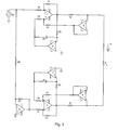
- a second embodiment of the present invention is illustrated as being configured for bipolar, low frequency AC operation into a resistive load.
- the second embodiment comprises the current source illustrated in FIG. 3 which has been modified to further include one or more features selected from the group consisting of range switching, and active common mode reduction.
- the current source illustrated in FIG. 4 further comprises sense resistors 25 & 26, and switching means known in the art (e.g., corresponding switches 40 & 41). Resistors 25 and 26 can be switched in to establish a new current range in comprising range switching in the current source.
- This embodiment is useful in applications where the output current changes over more than one order of magnitude or cannot be easily scaled by changing the control voltage Vc.
- active common mode reduction may comprise a means of sensing common mode voltage (e.g., resistors 27 & 28, or by other suitable means known in the art), a means of scaling the common mode voltage (e.g., resistor 24, or by other suitable means known in the art), a means of feeding back the scaled common mode voltage to bias the operating point of the current source (feeding back the result to op-amps 6 & 7, or by other suitable means known in the art), and a means of turning off common mode reduction for grounded load operation (e.g., reduction of resistor 24 to zero ohms or by other suitable means known in the art).
- common mode voltage e.g., resistors 27 & 28, or by other suitable means known in the art
- a means of scaling the common mode voltage e.g., resistor 24, or by other suitable means known in the art
- a means of feeding back the scaled common mode voltage to bias the operating point of the current source feeding back the result to op-amps 6 & 7, or by other
- Is Vc / R
- Vc a control voltage
- R a sense resistor 10
- Resistor 25 and switch 40 demonstrate a plurality of resistors and switches that can be used to change current by changing R on the first half of the current source.
- resistor 26 and switch 41 demonstrate a plurality of resistors and switches that can be used to change current by changing R on the second half of the current source.
- the common-mode reduction circuit actively cancels common mode voltages by reducing the output impedance of the current source to common mode signals while continuing to drive a floating load with high impedance.
- Resistors 27 and 28 feed the buffered voltage signals from amplifiers 2 and 4 to the inverting input of amplifier 8.
- This inverted, common-mode signal is fed to the non-inverting inputs of amplifiers 6 and 7.
- Resistors 27 and 28 are equal values for symmetry of action and the ratio of resistors 24 to resistors 27 and 28 can be scaled for different levels of reduction. Common mode reduction can be effectively turned off by reducing resistor 24 to 0 ohms. Capacitors 32, 33 and 34 provide stability at high frequencies.
Landscapes
- Engineering & Computer Science (AREA)
- Power Engineering (AREA)
- Amplifiers (AREA)
- Semiconductor Lasers (AREA)
- Continuous-Control Power Sources That Use Transistors (AREA)
- Control Of Voltage And Current In General (AREA)
Claims (6)
- Source de courant commandée en tension pour générer un courant de charge voulu qui circule à travers une impédance de charge sélectionnée (ZL), le courant de charge étant fonction d'une tension d'entrée délivrée et étant sensiblement indépendant de l'impédance de charge, la source de courant commandée en tension pouvant fonctionner comme une source de courant différentiel pour une charge flottante ou comme une source de courant de charge mise à la terre lorsqu'une extrémité de la charge est reliée à la terre, et la source de courant commandée en tension comportant :a) deux moitiés symétriques (1, 2, 6 et 3, 4, 7) qui commandent chaque extrémité de la charge,b) des moyens de centrage d'une tension de fonctionnement entre des rails d'alimentation en énergie (6, 14, 22, 30 et 7, 19, 23, 31), etc) des moyens de réduction de l'erreur DC de ladite source de courant commandée en tension sans ajustement manuel (6, 22, 30 et 7, 23, 31).
- Source de courant commandée en tension selon la revendication 1, dans laquelle la source de courant commandée en tension est configurée pour un fonctionnement sélectionné parmi le groupe constitué d'un fonctionnement à courant alternatif (AC), un fonctionnement à courant continu (DC), un fonctionnement unipolaire, un fonctionnement bipolaire, un fonctionnement avec une charge résistive, un fonctionnement avec une charge réactive, et une combinaison de ces derniers.
- Source de courant commandée en tension selon la revendication 1, comportant de plus une pluralité de résistances de détection et des moyens de commutation pour fournir une fonctionnalité de commutation de gammes.
- Source de courant commandée en tension selon la revendication 1, comportant de plus une réduction active de mode commun.
- Source de courant commandée en tension selon la revendication 1, comportant de plus :a) une pluralité de résistances de détection et des moyens de commutation pour fournir une fonctionnalité de commutation de gammes, etb) une réduction active de mode commun.
- Source de courant commandée en tension selon la revendication 5, dans laquelle la source de courant commandée en tension est configurée pour un fonctionnement sélectionné parmi le groupe constitué d'un fonctionnement à AC, un fonctionnement à DC, un fonctionnement unipolaire, un fonctionnement bipolaire, un fonctionnement avec une charge résistive, un fonctionnement avec une charge réactive, et une combinaison de ces derniers.
Applications Claiming Priority (5)
| Application Number | Priority Date | Filing Date | Title |
|---|---|---|---|
| US25221200P | 2000-11-21 | 2000-11-21 | |
| US252212P | 2000-11-21 | ||
| US09/971,274 US6501255B2 (en) | 2000-11-21 | 2001-10-04 | Differential current source with active common mode reduction |
| US971274 | 2001-10-04 | ||
| PCT/US2001/031524 WO2003054924A2 (fr) | 2000-11-21 | 2001-10-10 | Source de courant differentiel a reduction de tension de mode commun sous retroaction active |
Publications (3)
| Publication Number | Publication Date |
|---|---|
| EP1410126A2 EP1410126A2 (fr) | 2004-04-21 |
| EP1410126A4 EP1410126A4 (fr) | 2005-11-02 |
| EP1410126B1 true EP1410126B1 (fr) | 2006-12-27 |
Family
ID=26942125
Family Applications (1)
| Application Number | Title | Priority Date | Filing Date |
|---|---|---|---|
| EP01275082A Expired - Lifetime EP1410126B1 (fr) | 2000-11-21 | 2001-10-10 | Source de courant differentiel a reduction de tension de mode commun sous retroaction active |
Country Status (7)
| Country | Link |
|---|---|
| US (1) | US6501255B2 (fr) |
| EP (1) | EP1410126B1 (fr) |
| JP (1) | JP4109200B2 (fr) |
| AT (1) | ATE349731T1 (fr) |
| AU (1) | AU2001298059A1 (fr) |
| DE (1) | DE60125601T2 (fr) |
| WO (1) | WO2003054924A2 (fr) |
Families Citing this family (20)
| Publication number | Priority date | Publication date | Assignee | Title |
|---|---|---|---|---|
| US6667614B1 (en) * | 2000-02-16 | 2003-12-23 | Seagate Technology Llc | Transfer curve tester for testing magnetic recording heads |
| JP2002185275A (ja) * | 2000-10-06 | 2002-06-28 | Toshiba Corp | 可変利得増幅器 |
| JP2005102750A (ja) * | 2003-09-26 | 2005-04-21 | Olympus Corp | 電気手術用電源装置 |
| US7592790B2 (en) * | 2006-04-19 | 2009-09-22 | System General Corp. | Start-up circuit with feedforward compensation for power converters |
| JP2007324991A (ja) * | 2006-06-01 | 2007-12-13 | Victor Co Of Japan Ltd | 電流検出回路 |
| US7884593B2 (en) * | 2008-03-26 | 2011-02-08 | Quantum Design, Inc. | Differential and symmetrical current source |
| AU2010225277A1 (en) * | 2009-03-20 | 2011-11-10 | Rainer Ottis Seidl | Measurement system for evaluating the swallowing process and/or for detecting aspiration |
| US7876155B2 (en) * | 2009-05-16 | 2011-01-25 | Alcatel-Lucent Usa Inc. | Transimpedance amplifier with distributed control of feedback line |
| TW201126858A (en) * | 2010-01-19 | 2011-08-01 | Hon Hai Prec Ind Co Ltd | Current balance circuit |
| SK288245B6 (sk) * | 2010-09-03 | 2015-03-03 | Ivan Baĺ¤Ko | Prúdový zdroj s aktívnym potláčaním súčtového napätia |
| US8390374B2 (en) | 2011-01-25 | 2013-03-05 | Analog Devices, Inc. | Apparatus and method for amplification with high front-end gain in the presence of large DC offsets |
| EP2671612A1 (fr) | 2012-06-07 | 2013-12-11 | Nasesch GbR | Procédé de mesure de l'obstruction du pharynx au moyen d'une électrode combinée |
| US8823453B2 (en) * | 2012-11-07 | 2014-09-02 | Semtech Corporation | Instrumentation amplifier with rail-to-rail input range |
| GB2526630B (en) * | 2014-05-30 | 2016-05-04 | Contacta Systems Ltd | Amplifier for induction loop |
| CN106774576A (zh) * | 2016-09-28 | 2017-05-31 | 西安航天动力研究所 | 一种多路精密恒流源 |
| US11853089B2 (en) * | 2019-07-25 | 2023-12-26 | Keithley Instruments, Llc | Expanded shunt current source |
| CN111007913B (zh) * | 2019-12-05 | 2021-11-30 | 北京东方计量测试研究所 | 一种提升电流源稳定性的电路及方法 |
| EP4143976A4 (fr) | 2020-04-28 | 2023-11-01 | Lake Shore Cryotronics, Inc. | Systèmes et procédés de mesure de plage visant à atténuer les effets transitifs dans des mesures de matériaux à plages multiples |
| CN114217659A (zh) * | 2021-12-03 | 2022-03-22 | 国网浙江省电力有限公司建德市供电公司 | 一种压控交流恒流源电路及消弧线圈自动补偿校验装置 |
| CN118454105B (zh) * | 2024-04-23 | 2025-04-08 | 国家康复辅具研究中心 | 一种差分输出电流源电路及时域相干电刺激方法 |
Family Cites Families (6)
| Publication number | Priority date | Publication date | Assignee | Title |
|---|---|---|---|---|
| US4451779A (en) * | 1982-04-22 | 1984-05-29 | Honeywell Inc. | Voltage controlled current source |
| US5087890A (en) * | 1989-09-20 | 1992-02-11 | Sanyo Electric Co., Ltd. | Amplifier circuit |
| US5021729A (en) | 1989-10-06 | 1991-06-04 | The United States Of America As Represented By The Administrator Of The Administration National Aeronautics And Space | Differential current source |
| US5153499A (en) * | 1991-09-18 | 1992-10-06 | Allied-Signal Inc. | Precision voltage controlled current source with variable compliance |
| US5465041A (en) * | 1993-09-17 | 1995-11-07 | Penberthy, Inc. | Bipolar tracking current source/sink with ground clamp |
| JPH11205095A (ja) * | 1998-01-19 | 1999-07-30 | Nippon Precision Circuits Kk | 電圧制御発振回路 |
-
2001
- 2001-10-04 US US09/971,274 patent/US6501255B2/en not_active Expired - Lifetime
- 2001-10-10 EP EP01275082A patent/EP1410126B1/fr not_active Expired - Lifetime
- 2001-10-10 AU AU2001298059A patent/AU2001298059A1/en not_active Abandoned
- 2001-10-10 AT AT01275082T patent/ATE349731T1/de not_active IP Right Cessation
- 2001-10-10 JP JP2003555553A patent/JP4109200B2/ja not_active Expired - Lifetime
- 2001-10-10 DE DE60125601T patent/DE60125601T2/de not_active Expired - Lifetime
- 2001-10-10 WO PCT/US2001/031524 patent/WO2003054924A2/fr not_active Ceased
Also Published As
| Publication number | Publication date |
|---|---|
| JP4109200B2 (ja) | 2008-07-02 |
| US20020060915A1 (en) | 2002-05-23 |
| JP2005513657A (ja) | 2005-05-12 |
| US6501255B2 (en) | 2002-12-31 |
| ATE349731T1 (de) | 2007-01-15 |
| AU2001298059A1 (en) | 2003-07-09 |
| WO2003054924A3 (fr) | 2003-10-23 |
| DE60125601T2 (de) | 2007-10-11 |
| WO2003054924A2 (fr) | 2003-07-03 |
| EP1410126A2 (fr) | 2004-04-21 |
| DE60125601D1 (de) | 2007-02-08 |
| AU2001298059A8 (en) | 2003-07-09 |
| EP1410126A4 (fr) | 2005-11-02 |
Similar Documents
| Publication | Publication Date | Title |
|---|---|---|
| EP1410126B1 (fr) | Source de courant differentiel a reduction de tension de mode commun sous retroaction active | |
| EP0295221B1 (fr) | Amplificateur opérationnel de puissance CMOS | |
| DE69532093T2 (de) | Stromdetektorschaltungen | |
| EP0935849A1 (fr) | Etage de sortie cmos a faible impedance et procede associe | |
| US4091333A (en) | Transconductance amplifier circuit | |
| US5977757A (en) | Power supply having automatic voltage sensing | |
| JPH0666609B2 (ja) | 集積回路 | |
| EP2688203A2 (fr) | Amplificateur de transconductance à sorties multiples à base d'amplificateur d'instrumentation | |
| EP0502056B1 (fr) | Amplificateur differentiel avec reseau attenuateur d'entree | |
| US5115206A (en) | Merged differential amplifier and current source | |
| US4659997A (en) | Differential voltage measuring circuit | |
| US20090039862A1 (en) | Voltage transformation circuit | |
| US5781068A (en) | Transadmittance amplifier for a motor | |
| EP0816857B1 (fr) | Circuit de correction de réjection de mode commun pour atténuateur différentiel | |
| US12506470B2 (en) | Differential current buffer circuit and dc and alternating current source comprising the same | |
| US6680642B2 (en) | Analog bipolar current source | |
| US6211731B1 (en) | Impedance altering apparatus | |
| EP0171653A2 (fr) | Circuit multiplicateur analogique | |
| EP0426598B1 (fr) | Amplificateur à transistor ayant des circuits de polarisation variables | |
| DK168722B1 (da) | Differentialforstærkerkobling | |
| US7135920B2 (en) | Method and circuit for facilitating control of AC coupling in an amplifier circuit | |
| JPH0793543B2 (ja) | 電圧リピ−タ回路 | |
| EP1088393B1 (fr) | Systeme amplificateur | |
| Austin | Current Feedback Amplifiers: Review, Stability Analysis, and Applications | |
| KR0134577B1 (ko) | 증폭기 |
Legal Events
| Date | Code | Title | Description |
|---|---|---|---|
| PUAI | Public reference made under article 153(3) epc to a published international application that has entered the european phase |
Free format text: ORIGINAL CODE: 0009012 |
|
| 17P | Request for examination filed |
Effective date: 20030620 |
|
| AK | Designated contracting states |
Kind code of ref document: A2 Designated state(s): AT BE CH CY DE DK ES FI FR GB GR IE IT LI LU MC NL PT SE TR |
|
| A4 | Supplementary search report drawn up and despatched |
Effective date: 20050921 |
|
| RIC1 | Information provided on ipc code assigned before grant |
Ipc: 7H 03F 3/45 B Ipc: 7G 05F 3/04 A |
|
| GRAP | Despatch of communication of intention to grant a patent |
Free format text: ORIGINAL CODE: EPIDOSNIGR1 |
|
| GRAS | Grant fee paid |
Free format text: ORIGINAL CODE: EPIDOSNIGR3 |
|
| GRAA | (expected) grant |
Free format text: ORIGINAL CODE: 0009210 |
|
| AK | Designated contracting states |
Kind code of ref document: B1 Designated state(s): AT BE CH CY DE DK ES FI FR GB GR IE IT LI LU MC NL PT SE TR |
|
| PG25 | Lapsed in a contracting state [announced via postgrant information from national office to epo] |
Ref country code: IT Free format text: LAPSE BECAUSE OF FAILURE TO SUBMIT A TRANSLATION OF THE DESCRIPTION OR TO PAY THE FEE WITHIN THE PRESCRIBED TIME-LIMIT;WARNING: LAPSES OF ITALIAN PATENTS WITH EFFECTIVE DATE BEFORE 2007 MAY HAVE OCCURRED AT ANY TIME BEFORE 2007. THE CORRECT EFFECTIVE DATE MAY BE DIFFERENT FROM THE ONE RECORDED. Effective date: 20061227 Ref country code: AT Free format text: LAPSE BECAUSE OF FAILURE TO SUBMIT A TRANSLATION OF THE DESCRIPTION OR TO PAY THE FEE WITHIN THE PRESCRIBED TIME-LIMIT Effective date: 20061227 Ref country code: FI Free format text: LAPSE BECAUSE OF FAILURE TO SUBMIT A TRANSLATION OF THE DESCRIPTION OR TO PAY THE FEE WITHIN THE PRESCRIBED TIME-LIMIT Effective date: 20061227 Ref country code: DK Free format text: LAPSE BECAUSE OF FAILURE TO SUBMIT A TRANSLATION OF THE DESCRIPTION OR TO PAY THE FEE WITHIN THE PRESCRIBED TIME-LIMIT Effective date: 20061227 Ref country code: BE Free format text: LAPSE BECAUSE OF FAILURE TO SUBMIT A TRANSLATION OF THE DESCRIPTION OR TO PAY THE FEE WITHIN THE PRESCRIBED TIME-LIMIT Effective date: 20061227 Ref country code: NL Free format text: LAPSE BECAUSE OF FAILURE TO SUBMIT A TRANSLATION OF THE DESCRIPTION OR TO PAY THE FEE WITHIN THE PRESCRIBED TIME-LIMIT Effective date: 20061227 |
|
| REG | Reference to a national code |
Ref country code: GB Ref legal event code: FG4D |
|
| REG | Reference to a national code |
Ref country code: IE Ref legal event code: FG4D |
|
| REF | Corresponds to: |
Ref document number: 60125601 Country of ref document: DE Date of ref document: 20070208 Kind code of ref document: P |
|
| PG25 | Lapsed in a contracting state [announced via postgrant information from national office to epo] |
Ref country code: SE Free format text: LAPSE BECAUSE OF FAILURE TO SUBMIT A TRANSLATION OF THE DESCRIPTION OR TO PAY THE FEE WITHIN THE PRESCRIBED TIME-LIMIT Effective date: 20070327 |
|
| PG25 | Lapsed in a contracting state [announced via postgrant information from national office to epo] |
Ref country code: ES Free format text: LAPSE BECAUSE OF FAILURE TO SUBMIT A TRANSLATION OF THE DESCRIPTION OR TO PAY THE FEE WITHIN THE PRESCRIBED TIME-LIMIT Effective date: 20070407 |
|
| REG | Reference to a national code |
Ref country code: CH Ref legal event code: NV Representative=s name: MICHELI & CIE SA |
|
| PG25 | Lapsed in a contracting state [announced via postgrant information from national office to epo] |
Ref country code: PT Free format text: LAPSE BECAUSE OF FAILURE TO SUBMIT A TRANSLATION OF THE DESCRIPTION OR TO PAY THE FEE WITHIN THE PRESCRIBED TIME-LIMIT Effective date: 20070528 |
|
| NLV1 | Nl: lapsed or annulled due to failure to fulfill the requirements of art. 29p and 29m of the patents act | ||
| ET | Fr: translation filed | ||
| PLBE | No opposition filed within time limit |
Free format text: ORIGINAL CODE: 0009261 |
|
| STAA | Information on the status of an ep patent application or granted ep patent |
Free format text: STATUS: NO OPPOSITION FILED WITHIN TIME LIMIT |
|
| 26N | No opposition filed |
Effective date: 20070928 |
|
| PG25 | Lapsed in a contracting state [announced via postgrant information from national office to epo] |
Ref country code: GR Free format text: LAPSE BECAUSE OF FAILURE TO SUBMIT A TRANSLATION OF THE DESCRIPTION OR TO PAY THE FEE WITHIN THE PRESCRIBED TIME-LIMIT Effective date: 20070328 |
|
| PG25 | Lapsed in a contracting state [announced via postgrant information from national office to epo] |
Ref country code: MC Free format text: LAPSE BECAUSE OF NON-PAYMENT OF DUE FEES Effective date: 20071031 |
|
| PG25 | Lapsed in a contracting state [announced via postgrant information from national office to epo] |
Ref country code: IE Free format text: LAPSE BECAUSE OF NON-PAYMENT OF DUE FEES Effective date: 20071010 |
|
| PG25 | Lapsed in a contracting state [announced via postgrant information from national office to epo] |
Ref country code: CY Free format text: LAPSE BECAUSE OF FAILURE TO SUBMIT A TRANSLATION OF THE DESCRIPTION OR TO PAY THE FEE WITHIN THE PRESCRIBED TIME-LIMIT Effective date: 20061227 Ref country code: LU Free format text: LAPSE BECAUSE OF NON-PAYMENT OF DUE FEES Effective date: 20071010 |
|
| PG25 | Lapsed in a contracting state [announced via postgrant information from national office to epo] |
Ref country code: TR Free format text: LAPSE BECAUSE OF FAILURE TO SUBMIT A TRANSLATION OF THE DESCRIPTION OR TO PAY THE FEE WITHIN THE PRESCRIBED TIME-LIMIT Effective date: 20061227 |
|
| REG | Reference to a national code |
Ref country code: FR Ref legal event code: PLFP Year of fee payment: 16 |
|
| REG | Reference to a national code |
Ref country code: FR Ref legal event code: PLFP Year of fee payment: 17 |
|
| REG | Reference to a national code |
Ref country code: FR Ref legal event code: PLFP Year of fee payment: 18 |
|
| PGFP | Annual fee paid to national office [announced via postgrant information from national office to epo] |
Ref country code: FR Payment date: 20200904 Year of fee payment: 20 |
|
| PGFP | Annual fee paid to national office [announced via postgrant information from national office to epo] |
Ref country code: CH Payment date: 20201022 Year of fee payment: 20 Ref country code: DE Payment date: 20200922 Year of fee payment: 20 Ref country code: GB Payment date: 20201028 Year of fee payment: 20 |
|
| REG | Reference to a national code |
Ref country code: DE Ref legal event code: R071 Ref document number: 60125601 Country of ref document: DE |
|
| REG | Reference to a national code |
Ref country code: CH Ref legal event code: PL |
|
| REG | Reference to a national code |
Ref country code: GB Ref legal event code: PE20 Expiry date: 20211009 |
|
| PG25 | Lapsed in a contracting state [announced via postgrant information from national office to epo] |
Ref country code: GB Free format text: LAPSE BECAUSE OF EXPIRATION OF PROTECTION Effective date: 20211009 |