EP1408724A1 - Circuit formed substrate and method of manufacturing circuit formed substrate - Google Patents
Circuit formed substrate and method of manufacturing circuit formed substrate Download PDFInfo
- Publication number
- EP1408724A1 EP1408724A1 EP02746094A EP02746094A EP1408724A1 EP 1408724 A1 EP1408724 A1 EP 1408724A1 EP 02746094 A EP02746094 A EP 02746094A EP 02746094 A EP02746094 A EP 02746094A EP 1408724 A1 EP1408724 A1 EP 1408724A1
- Authority
- EP
- European Patent Office
- Prior art keywords
- thickness
- reinforcing member
- board
- prepreg
- board material
- Prior art date
- Legal status (The legal status is an assumption and is not a legal conclusion. Google has not performed a legal analysis and makes no representation as to the accuracy of the status listed.)
- Withdrawn
Links
Images


Classifications
-
- H—ELECTRICITY
- H05—ELECTRIC TECHNIQUES NOT OTHERWISE PROVIDED FOR
- H05K—PRINTED CIRCUITS; CASINGS OR CONSTRUCTIONAL DETAILS OF ELECTRIC APPARATUS; MANUFACTURE OF ASSEMBLAGES OF ELECTRICAL COMPONENTS
- H05K3/00—Apparatus or processes for manufacturing printed circuits
- H05K3/40—Forming printed elements for providing electric connections to or between printed circuits
- H05K3/4038—Through-connections; Vertical interconnect access [VIA] connections
- H05K3/4053—Through-connections; Vertical interconnect access [VIA] connections by thick-film techniques
- H05K3/4069—Through-connections; Vertical interconnect access [VIA] connections by thick-film techniques for via connections in organic insulating substrates
-
- H—ELECTRICITY
- H05—ELECTRIC TECHNIQUES NOT OTHERWISE PROVIDED FOR
- H05K—PRINTED CIRCUITS; CASINGS OR CONSTRUCTIONAL DETAILS OF ELECTRIC APPARATUS; MANUFACTURE OF ASSEMBLAGES OF ELECTRICAL COMPONENTS
- H05K1/00—Printed circuits
- H05K1/02—Details
- H05K1/03—Use of materials for the substrate
- H05K1/0313—Organic insulating material
- H05K1/0353—Organic insulating material consisting of two or more materials, e.g. two or more polymers, polymer + filler, + reinforcement
- H05K1/0366—Organic insulating material consisting of two or more materials, e.g. two or more polymers, polymer + filler, + reinforcement reinforced, e.g. by fibres, fabrics
-
- H—ELECTRICITY
- H05—ELECTRIC TECHNIQUES NOT OTHERWISE PROVIDED FOR
- H05K—PRINTED CIRCUITS; CASINGS OR CONSTRUCTIONAL DETAILS OF ELECTRIC APPARATUS; MANUFACTURE OF ASSEMBLAGES OF ELECTRICAL COMPONENTS
- H05K2201/00—Indexing scheme relating to printed circuits covered by H05K1/00
- H05K2201/02—Fillers; Particles; Fibers; Reinforcement materials
- H05K2201/0275—Fibers and reinforcement materials
- H05K2201/0278—Polymeric fibers
-
- H—ELECTRICITY
- H05—ELECTRIC TECHNIQUES NOT OTHERWISE PROVIDED FOR
- H05K—PRINTED CIRCUITS; CASINGS OR CONSTRUCTIONAL DETAILS OF ELECTRIC APPARATUS; MANUFACTURE OF ASSEMBLAGES OF ELECTRICAL COMPONENTS
- H05K2201/00—Indexing scheme relating to printed circuits covered by H05K1/00
- H05K2201/02—Fillers; Particles; Fibers; Reinforcement materials
- H05K2201/0275—Fibers and reinforcement materials
- H05K2201/029—Woven fibrous reinforcement or textile
-
- H—ELECTRICITY
- H05—ELECTRIC TECHNIQUES NOT OTHERWISE PROVIDED FOR
- H05K—PRINTED CIRCUITS; CASINGS OR CONSTRUCTIONAL DETAILS OF ELECTRIC APPARATUS; MANUFACTURE OF ASSEMBLAGES OF ELECTRICAL COMPONENTS
- H05K2201/00—Indexing scheme relating to printed circuits covered by H05K1/00
- H05K2201/03—Conductive materials
- H05K2201/0332—Structure of the conductor
- H05K2201/0335—Layered conductors or foils
- H05K2201/0355—Metal foils
-
- H—ELECTRICITY
- H05—ELECTRIC TECHNIQUES NOT OTHERWISE PROVIDED FOR
- H05K—PRINTED CIRCUITS; CASINGS OR CONSTRUCTIONAL DETAILS OF ELECTRIC APPARATUS; MANUFACTURE OF ASSEMBLAGES OF ELECTRICAL COMPONENTS
- H05K2203/00—Indexing scheme relating to apparatus or processes for manufacturing printed circuits covered by H05K3/00
- H05K2203/14—Related to the order of processing steps
- H05K2203/1461—Applying or finishing the circuit pattern after another process, e.g. after filling of vias with conductive paste, after making printed resistors
-
- H—ELECTRICITY
- H05—ELECTRIC TECHNIQUES NOT OTHERWISE PROVIDED FOR
- H05K—PRINTED CIRCUITS; CASINGS OR CONSTRUCTIONAL DETAILS OF ELECTRIC APPARATUS; MANUFACTURE OF ASSEMBLAGES OF ELECTRICAL COMPONENTS
- H05K3/00—Apparatus or processes for manufacturing printed circuits
- H05K3/46—Manufacturing multilayer circuits
- H05K3/4611—Manufacturing multilayer circuits by laminating two or more circuit boards
- H05K3/4614—Manufacturing multilayer circuits by laminating two or more circuit boards the electrical connections between the circuit boards being made during lamination
-
- H—ELECTRICITY
- H05—ELECTRIC TECHNIQUES NOT OTHERWISE PROVIDED FOR
- H05K—PRINTED CIRCUITS; CASINGS OR CONSTRUCTIONAL DETAILS OF ELECTRIC APPARATUS; MANUFACTURE OF ASSEMBLAGES OF ELECTRICAL COMPONENTS
- H05K3/00—Apparatus or processes for manufacturing printed circuits
- H05K3/46—Manufacturing multilayer circuits
- H05K3/4644—Manufacturing multilayer circuits by building the multilayer layer by layer, i.e. build-up multilayer circuits
- H05K3/4652—Adding a circuit layer by laminating a metal foil or a preformed metal foil pattern
-
- Y—GENERAL TAGGING OF NEW TECHNOLOGICAL DEVELOPMENTS; GENERAL TAGGING OF CROSS-SECTIONAL TECHNOLOGIES SPANNING OVER SEVERAL SECTIONS OF THE IPC; TECHNICAL SUBJECTS COVERED BY FORMER USPC CROSS-REFERENCE ART COLLECTIONS [XRACs] AND DIGESTS
- Y10—TECHNICAL SUBJECTS COVERED BY FORMER USPC
- Y10S—TECHNICAL SUBJECTS COVERED BY FORMER USPC CROSS-REFERENCE ART COLLECTIONS [XRACs] AND DIGESTS
- Y10S428/00—Stock material or miscellaneous articles
- Y10S428/901—Printed circuit
-
- Y—GENERAL TAGGING OF NEW TECHNOLOGICAL DEVELOPMENTS; GENERAL TAGGING OF CROSS-SECTIONAL TECHNOLOGIES SPANNING OVER SEVERAL SECTIONS OF THE IPC; TECHNICAL SUBJECTS COVERED BY FORMER USPC CROSS-REFERENCE ART COLLECTIONS [XRACs] AND DIGESTS
- Y10—TECHNICAL SUBJECTS COVERED BY FORMER USPC
- Y10T—TECHNICAL SUBJECTS COVERED BY FORMER US CLASSIFICATION
- Y10T29/00—Metal working
- Y10T29/49—Method of mechanical manufacture
- Y10T29/49002—Electrical device making
- Y10T29/49117—Conductor or circuit manufacturing
- Y10T29/49124—On flat or curved insulated base, e.g., printed circuit, etc.
- Y10T29/49126—Assembling bases
-
- Y—GENERAL TAGGING OF NEW TECHNOLOGICAL DEVELOPMENTS; GENERAL TAGGING OF CROSS-SECTIONAL TECHNOLOGIES SPANNING OVER SEVERAL SECTIONS OF THE IPC; TECHNICAL SUBJECTS COVERED BY FORMER USPC CROSS-REFERENCE ART COLLECTIONS [XRACs] AND DIGESTS
- Y10—TECHNICAL SUBJECTS COVERED BY FORMER USPC
- Y10T—TECHNICAL SUBJECTS COVERED BY FORMER US CLASSIFICATION
- Y10T428/00—Stock material or miscellaneous articles
- Y10T428/24—Structurally defined web or sheet [e.g., overall dimension, etc.]
- Y10T428/24802—Discontinuous or differential coating, impregnation or bond [e.g., artwork, printing, retouched photograph, etc.]
- Y10T428/24917—Discontinuous or differential coating, impregnation or bond [e.g., artwork, printing, retouched photograph, etc.] including metal layer
Definitions
- the present invention relates to circuit boards used in various electronic apparatuses, it also relates to methods of manufacturing the same circuit boards.
- Board material 1 shown in Fig. 3A is so called prepreg that is formed by the following method: Woven fabric, as a reinforcing member to be used in circuit boards, is impregnated with thermosetting epoxy resin and turned into a status called stage B. Board material 1 is coated with film 2 on both the upper and rear faces by a laminating method using a heated roll.
- via holes 3 are formed through board material 1 with laser-beam, then via holes 3 are filled with conductive paste 4 produced by mixing conductive particles such as copper powder with thermosetting resin, curing agent, and solvent.
- Board material 1 thus becomes as shown in Fig. 3C.
- Films 2 are peeled off from both the faces, so that conductive paste 4 protrudes as shown in Fig. 3D.
- copper foils 5 are prepared, and hot-pressed by a hot-presser (not shown), so that material 1 is thermally cured as shown in Fig. 3E, and conductive paste 4 is compressed, thereby connecting copper foil 5 on the upper face to that on the rear face.
- the epoxy resin impregnated in material 1 flows outside and forms flow-out section 6. Surplus portions on both the ends of material 1 are cut off, so that the shape shown in Fig. 3F is formed. Then copper foils 5 are processed into desired patterns by etching or other methods to form circuit 7, and finally, the double-sided circuit board as shown in Fig. 3G is obtained.
- the foregoing method of manufacturing the circuit boards sometimes has instability about electrical connection with conductive paste between an upper-face circuit and a rear-face circuit of the circuit board as well as between an upper-face circuit and an inner circuit in the case of multi-layer circuit boards.
- the inventors have analyzed circuit boards manufactured or made on trial basis in order to investigate the causes of the instability discussed above.
- the result finds that conductive particles in conductive paste 4 flow out from via holes 3 and become flow-out particles 8 as shown in Fig. 3E.
- conductive paste 4 should be compressed vertically in Fig. 3 so that conductive particles in paste 4 contact with each other efficiently and firmly, and also contact with copper foil 5 firmly.
- flow-out section 6 is formed, so that thermosetting resin in board material 1 flows toward outer open ends during the heat and compression.
- the conductive particles in conductive paste 4 are pushed by the flowing thermosetting resin, and the particles flow laterally in Fig. 3.
- conductive paste 4 is not efficiently compressed, so that the electrical connections with conductive paste 4 become unstable.
- the foregoing description refers to the board material made of glass woven fabric and thermosetting resin.
- failures are also observed when other materials are used, such as inorganic fiber other than glass, or organic fiber such as aramid fiber, or a reinforcing member made of non-woven fabric other than woven fabric.
- thermosetting resin becomes so fluid that the conductive paste cannot achieve the electrical connection.
- the inventors have carried out various experiments and analyzed around the via holes having insufficient electrical connections. The result finds that flow-out particles as shown in Fig. 3E are observed more on the upper face than the rear face of board material 1. The inventors have investigated the causes of this status, and reached the following conclusion.
- board material 1 is manufactured by the following steps:
- the prepreg is completely cured by heat and press, i.e., the prepreg is turned into stage C. Then the prepreg is pierced with a drill before plated with a metal such as copper. As a result, layer-to-layer connection is achieved. Thus there is no such a problem as discussed above.
- conductive material namely, conductive paste is filled into via holes formed in board material in stage B so that connection between layers may be achieved. In this method the foregoing problem has occurred.
- a variety of thickness is required design-wise to insulating respective layers from each other of a circuit board; however, the reinforcing members to be used in prepreg have a limited number of thickness. Such a present situation obliges some manufacturers to use the board materials using impregnating resin 10, shown in Fig. 4, of which layer is even rather thick.
- the thickness ratio is, a thickness of a section of which major component is impregnated resin disposed on and beneath reinforcing member, namely, disposed near to the surface of board material, vs. a thickness of a center section, where the impregnated resin is merged with the reinforcing member, of the board material.
- connecting means between layers, such as conductive particles would flow out around the surface of the board material during the step of applying heat & press due to flow-out of the board material component.
- the method of the present invention for manufacturing the circuit boards uses the board material in stage B, which includes woven fabric, non-woven fabric, or mixed material of those two as a reinforcing member.
- the board material in stage B undergone a molding process is modified to have a thickness not less than the thickness of the reinforcing member and not more than 1.5 times that of the reinforcing member.
- the reinforcing member among the materials for the circuit board of the present invention takes not less than 30% and not more than 60% in total weight, or the thickness of the reinforcing member takes not less than 50% and not more than 90% out of the thickness of the board material.
- the present invention allows the connecting means, such as conductive paste, for realizing connection between layers to achieve the connection efficiently.
- the present invention can increase the reliability in electrical connection with conductive paste disposed between layers, and provide denser and quality circuit-forming boards.
- the present invention includes a step of layering at least two kinds of metallic foils and board materials into a layered body.
- One of the at least two is selected from the group consisting of metal foil, metal foil affixed to a supporter, and metal foil affixed to the supporter and formed with a circuit pattern.
- the other one includes at least one board material in stage B selected from the group consisting of (a) board material in stage B and having connecting means for connecting a layer to another layer, (b) board material in stage B and having a circuit pattern or metal foil and the connecting means, and (c) one of board material in stage C having a circuit or metal foil, or board material in stage C having a circuit or metal foil and the connecting means.
- the step of layering includes a step of applying heat and press.
- the board material in stage B includes woven fabric, non-woven fabric, or mixed material of those two fabrics as a reinforcing member, and this board material undergoes the step of heat & press, so that a thickness thereof in stage B becomes at least equal to and not more than 1.5 times of a thickness of the reinforcing member.
- a method of manufacturing the circuit board includes a step of applying heat & press, where electrical connections between layers can be achieved efficiently with layer-to-layer connecting means.
- the method of manufacturing the circuit board uses conductive material filled in via holes or non-via holes as the layer-to-layer connecting means, the via holes or the non-via-holes being provided to the board material in stage B.
- the conductive material is compressed efficiently during the step of applying heat & press, so that a layer-to-layer connection with a lower resistance is obtainable.
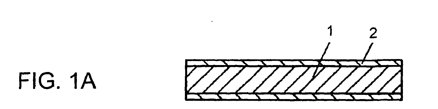
- Fig. 1A - Fig. 1G show sectional views illustrating a manufacturing method and materials of a circuit-forming board in accordance with the first exemplary embodiment of the present invention.
- film 2 of 20 ⁇ m thick adheres to both the faces of board material 1, which is prepreg using woven fabric made of glass fiber.
- board material 1 which is prepreg using woven fabric made of glass fiber.
- a nominal thickness that is often used to express a thickness is used.
- Film 2 uses polyethylene terephthalate (PET) of 20 ⁇ m thick; however, thermosetting resin such as epoxy resin can be coated on the board material as film 2 instead of the PET film.
- PET polyethylene terephthalate
- board material 1 is pierced with carbon dioxide gas laser, thereby having via holes of approx. 200 ⁇ m across.
- Conductive paste 4 is made by mixing copper powder having approx. 5 ⁇ m diameter with thermosetting resin and curing agent. Solvent can be added to paste 4 in order to adjust the viscosity.
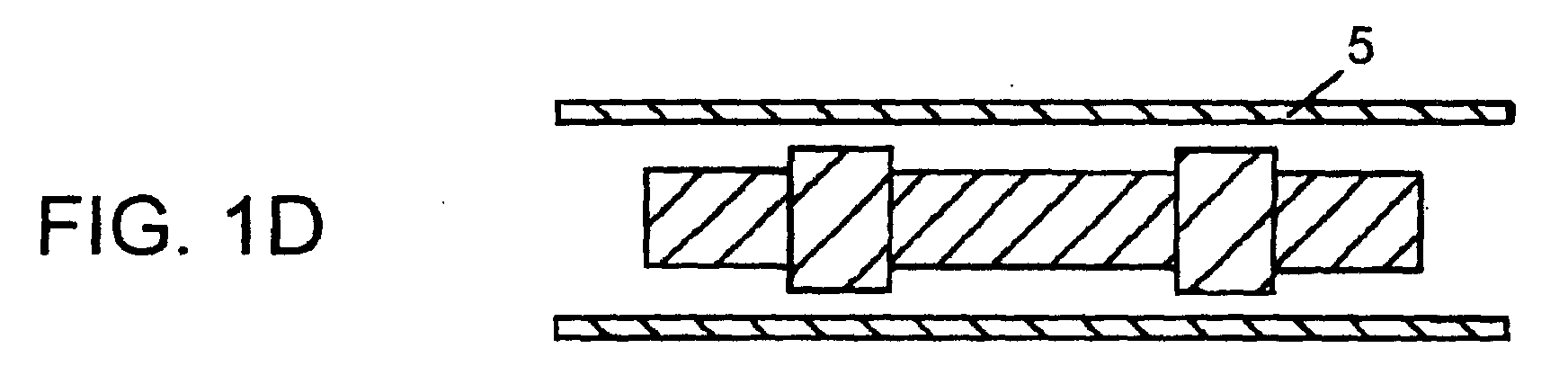
- film 2 on both the faces of board material 1 is peeled off, so that conductive paste 4 projects from material 1 by the thickness corresponding to the thickness of film 2.
- copper foil 5 is placed on both the faces of material 1.
- board material 1 undergoes the step of applying heat & press, where heat and press are applied to material 1 in a thickness direction of material 1, so that material 1 shapes in what is shown in Fig. 1E. At this time, the thermosetting resin in material 1 flows out and forms flow-out section 6.
- Plain weave glass-fiber fabrics of 60, 80, and 100 ⁇ m thick are prepared as reinforcing members. Those fabrics are generally used for ordinary printed circuit boards.
- An amount of thermosetting resin to be impregnated into the reinforcing members is expressed in a weight ratio. The resin impregnated is put in a dryer and turned into stage B, so that prepreg is produced. A thickness of the board after the step of heat & press is measured, and a ratio of this thickness vs. a thickness of glass-fiber woven cloth is calculated.
- a test pattern is formed on both the faces of the double-sided board produced. This test pattern has 500 layer-to-layer connections in series through the via holes of 200 ⁇ m across.
- connection resistance i.e., an electrical resistance between an upper face and a rear face per layer-to-layer connection is averaged out, and the resulting resistance value is referred to as a via-resistance value.
- Thickness of glass-fiber woven fabric T1 ( ⁇ m) Thickness of prepreg ( ⁇ m) Thickness of board material after heat & press T2 ( ⁇ m) Thickness ratio T2/T1 via-resistance value (m ⁇ ) 1 60 94 70 1.17 3 2 60 112 95 1.58 30 3 60 133 115 1.92 large dispersion 4 80 120 105 1.31 3.8 5 100 165 125 1.25 4.5 6 100 185 155 1.55 120 As Table 1 tells, when thickness T2 of board material 1 undergone the step of heat & press is not more than 1.5 times of thickness T1 of glass-fiber woven fabric, the via-resistance becomes stable.
- the sample of test No. 1 shows that although the via-resistance is low, a peel withstanding strength of copper foil 5 from board material 1 decreases to a lower level than a normal one. Thus if this sample is used in an application where a particular peel strength is required, an amount of resin is preferably added in order to increase the weight ratio from 66% to 67 - 68%.
- the sample of test No. 2 shows that the via-resistance increases when the sample undergoes a storage reliability test in a condition of high-temperature and high-humidity.
- the via-resistance is preferably not more than 10 m ⁇ .
- the thickness of the board after the heat & press preferably measures such that the ratio of T2/T1 becomes not more than 1.5.
- board material 1 in the status shown in Fig. 1E becomes thinner after the press, the electrical connection becomes better.
- board material 1 after the press needs at least the thickness of the reinforcing member because of the following reasons: (a) peel withstanding strength, (b) moldability in the step of heat & press, and (c) necessity of absorbing bumps and dips due to circuits on inner layers in the case of manufacturing multi-layer circuit boards.
- a ratio of the reinforcing member in the board material preferably ranges from not less than 30% to not more than 60% in weight ratio;
- a thickness of board material 1 in the status shown in Fig. 1A is set at the multiple from 1.1 to 2 of a thickness of the reinforcing member, namely, the thickness of the reinforcing material is adjusted to range from 50% to 90% that of board material 1.
- the first embodiment refers to the double-sided circuit board
- this second exemplary embodiment describes the case of manufacturing multi-layer circuit boards.
- the method of manufacturing the circuit boards and the materials thereof of the present invention can be used, and excellent electrical connections between layers are obtainable.
- Double-sided circuit board 11 used in this second embodiment can be a similar one to what is used in the first embodiment; however, a board having layer-to-layer connections formed by an ordinary plating method can be used. Also, a structure, where board material 1 is temporarily press-fitted to double-sided board 11 in the status shown in Fig. 2B, can be used.
- a method of manufacturing the multi-layer circuit boards is demonstrated hereinafter.
- film 2, board material 1, circuit board 7, board material 1, and film 2 are laminated in this order as shown in Fig. 1A - 1G.
- via holes 3 are formed with laser beam, and conductive paste 4 is filled in via holes 3.
- Film 2 is then peeled off, and copper foil 5 is disposed outside before heat & press are applied.
- the prepreg used in the first and the second embodiments is, for instance, ordinary glass-fiber woven fabric or non-woven fabric, either one is impregnated with thermosetting resin and turned into stage B.
- an organic fiber such as aramid fiber can be used.
- a material made by mixing woven fabric with non-woven fabric for instance, a material made by sandwiching glass-fiber non-woven fabric between two sheets of glass fibers can be used as a reinforcing member.
- thermosetting resin used in the previous embodiments includes sole resin, thermosetting resin composition made by mixing two or more than two materials, or the thermosetting resin composition modified by thermoplastic resin, such as: epoxy resin, epoxy-melamine based resin, unsaturated polyester based resin, phenol based resin, polyimide based resin, cyanate-system resin, ester cyanate based resin, naphtalene based resin, urea resin, amino resin, alkyd resin, silicone resin, furan nased resin, polyurethane resin, aminoalkyd resin, acrylic resin, fluoro resin, polyphenylene ether resin, ester cyanate resin, and the like. Fire retardant additive or inorganic filler can be added to those resins when necessary.
- thermoplastic resin such as: epoxy resin, epoxy-melamine based resin, unsaturated polyester based resin, phenol based resin, polyimide based resin, cyanate-system resin, ester cyanate based resin, naphtalene based resin, urea resin, amino resin
- a circuit made from metal foil temporarily attached to a supporter can be used.
- the conductive paste is used as means for connecting a layer to another layer.
- the paste is made by mixing conductive particles such as copper powder with thermosetting resin including curing agent. Besides those ingredients, the conductive paste can be made by mixing the conductive particles with polymeric material or solvent of an appropriate viscosity, or can be formed of various combinations of other ingredients.
- a conductive projection formed by plating, or conductive particles, not in pasted condition, having a rather large diameter can be used independently as the means for connecting a layer to another layer.
- a manufacturing method of circuit-forming boards and the circuit-forming board are provided.
- a thickness of board material where connecting means for connecting a layer to another layer are available is at least equal to and not more than 1.5 times of a thickness of a reinforcing member. This structure allows the connecting means such as conductive paste to connect the layers effectively
- a use of woven fabric, which employs fibers such as glass, as a reinforcing member to prepreg used as board material stabilizes layer-to-layer connection making full use of advantages such as dimensional stability of the woven fabric and strength of copper foil against being peeled off.
- an amount of the reinforcing member in the board material is set to range from not less than 30% to not more than 60% in weight ratio, or a thickness of the reinforcing member is set to range from not less than 50% to not more than 90% that of the board material.
Landscapes
- Engineering & Computer Science (AREA)
- Microelectronics & Electronic Packaging (AREA)
- Manufacturing & Machinery (AREA)
- Production Of Multi-Layered Print Wiring Board (AREA)
- Printing Elements For Providing Electric Connections Between Printed Circuits (AREA)
Abstract
A circuit board ensuring electrical connections is provided. An
insulated board material, having connecting means for connecting a layer to
another layer, includes a reinforcing member. A thickness of the entire
insulated board material is at least equal to or not more than 1.5 times of a
thickness of the reinforcing member.




Description
The present invention relates to circuit boards used in various
electronic apparatuses, it also relates to methods of manufacturing the same
circuit boards.
Electronic apparatuses have been downsized and become denser in
packaging. This market trend involves circuit-forming boards, to which
electronic components are to be mounted, to be double-sided boards, or multi-layer
boards. As such, higher density boards that can accommodate more
circuits and more components are developed. (e.g., Refer to "Surface
Mounting Technique" January 1997, published by Daily Industry Newspaper
Inc. in Japan. This edition includes a paper titled "Remarkable Development
of Build-up Multi-layer PWB" written by Mr. Kiyoshi Takagi.)
Prior art is described hereinafter with reference to Fig. 3 and Fig. 4.
Board material 1 shown in Fig. 3A is so called prepreg that is formed by the
following method: Woven fabric, as a reinforcing member to be used in circuit
boards, is impregnated with thermosetting epoxy resin and turned into a
status called stage B. Board material 1 is coated with film 2 on both the
upper and rear faces by a laminating method using a heated roll.
Next, as shown in Fig. 3B, via holes 3 are formed through board
material 1 with laser-beam, then via holes 3 are filled with conductive paste 4
produced by mixing conductive particles such as copper powder with
thermosetting resin, curing agent, and solvent. Board material 1 thus
becomes as shown in Fig. 3C. Films 2 are peeled off from both the faces, so
that conductive paste 4 protrudes as shown in Fig. 3D. Above both the faces
of material 1, copper foils 5 are prepared, and hot-pressed by a hot-presser
(not shown), so that material 1 is thermally cured as shown in Fig. 3E, and
conductive paste 4 is compressed, thereby connecting copper foil 5 on the
upper face to that on the rear face. At this time, the epoxy resin
impregnated in material 1 flows outside and forms flow-out section 6.
Surplus portions on both the ends of material 1 are cut off, so that the shape
shown in Fig. 3F is formed. Then copper foils 5 are processed into desired
patterns by etching or other methods to form circuit 7, and finally, the double-sided
circuit board as shown in Fig. 3G is obtained.
The foregoing method of manufacturing the circuit boards, however,
sometimes has instability about electrical connection with conductive paste
between an upper-face circuit and a rear-face circuit of the circuit board as
well as between an upper-face circuit and an inner circuit in the case of
multi-layer circuit boards.
The inventors have analyzed circuit boards manufactured or made on
trial basis in order to investigate the causes of the instability discussed above.
The result finds that conductive particles in conductive paste 4 flow out from
via holes 3 and become flow-out particles 8 as shown in Fig. 3E.
In other words, conductive paste 4 should be compressed vertically in
Fig. 3 so that conductive particles in paste 4 contact with each other efficiently
and firmly, and also contact with copper foil 5 firmly. However, in the process
between Fig. 3D and Fig. 3E, flow-out section 6 is formed, so that
thermosetting resin in board material 1 flows toward outer open ends during
the heat and compression. At that time, the conductive particles in
conductive paste 4 are pushed by the flowing thermosetting resin, and the
particles flow laterally in Fig. 3. As a result, conductive paste 4 is not
efficiently compressed, so that the electrical connections with conductive paste
4 become unstable. The foregoing description refers to the board material
made of glass woven fabric and thermosetting resin. However, failures are
also observed when other materials are used, such as inorganic fiber other
than glass, or organic fiber such as aramid fiber, or a reinforcing member
made of non-woven fabric other than woven fabric.
When woven fabric is used among others, flow resistance becomes small
due to the structure using the woven fabric. Thus the thermosetting resin
becomes so fluid that the conductive paste cannot achieve the electrical
connection.
The inventors have carried out various experiments and analyzed
around the via holes having insufficient electrical connections. The result
finds that flow-out particles as shown in Fig. 3E are observed more on the
upper face than the rear face of board material 1. The inventors have
investigated the causes of this status, and reached the following conclusion.
In the case where prepreg employing the woven fabric made of glass
fiber is used as board material, the board material has the sectional view as
shown in Fig. 4. In other words, board material 1 is manufactured by the
following steps:
In the case where regular prepreg is used as the material of circuit
boards, the prepreg is completely cured by heat and press, i.e., the prepreg is
turned into stage C. Then the prepreg is pierced with a drill before plated
with a metal such as copper. As a result, layer-to-layer connection is
achieved. Thus there is no such a problem as discussed above. Recently a
manufacturing method of high-density circuit-forming boards has been
developed, the method teaches that conductive material, namely, conductive
paste is filled into via holes formed in board material in stage B so that
connection between layers may be achieved. In this method the foregoing
problem has occurred.
A variety of thickness is required design-wise to insulating respective
layers from each other of a circuit board; however, the reinforcing members to
be used in prepreg have a limited number of thickness. Such a present
situation obliges some manufacturers to use the board materials using
impregnating resin 10, shown in Fig. 4, of which layer is even rather thick.
Through numerous experiments and analyses of samples, the inventors
have found that maintaining the following thickness ratio at an appropriate
level is crucial to solve the problem discussed previously. The thickness ratio
is, a thickness of a section of which major component is impregnated resin
disposed on and beneath reinforcing member, namely, disposed near to the
surface of board material, vs. a thickness of a center section, where the
impregnated resin is merged with the reinforcing member, of the board
material. In other words, if the thickness ratio is not appropriate, connecting
means between layers, such as conductive particles, would flow out around
the surface of the board material during the step of applying heat & press due
to flow-out of the board material component.
The method of the present invention for manufacturing the circuit
boards uses the board material in stage B, which includes woven fabric, non-woven
fabric, or mixed material of those two as a reinforcing member. The
board material in stage B undergone a molding process is modified to have a
thickness not less than the thickness of the reinforcing member and not more
than 1.5 times that of the reinforcing member.
The reinforcing member among the materials for the circuit board of
the present invention takes not less than 30% and not more than 60% in total
weight, or the thickness of the reinforcing member takes not less than 50%
and not more than 90% out of the thickness of the board material.
The present invention allows the connecting means, such as conductive
paste, for realizing connection between layers to achieve the connection
efficiently.
As a result, the present invention can increase the reliability in
electrical connection with conductive paste disposed between layers, and
provide denser and quality circuit-forming boards.
The present invention includes a step of layering at least two kinds of
metallic foils and board materials into a layered body. One of the at least two
is selected from the group consisting of metal foil, metal foil affixed to a
supporter, and metal foil affixed to the supporter and formed with a circuit
pattern. The other one includes at least one board material in stage B
selected from the group consisting of (a) board material in stage B and having
connecting means for connecting a layer to another layer, (b) board material in
stage B and having a circuit pattern or metal foil and the connecting means,
and (c) one of board material in stage C having a circuit or metal foil, or board
material in stage C having a circuit or metal foil and the connecting means.
The step of layering includes a step of applying heat and press. The
board material in stage B includes woven fabric, non-woven fabric, or mixed
material of those two fabrics as a reinforcing member, and this board material
undergoes the step of heat & press, so that a thickness thereof in stage B
becomes at least equal to and not more than 1.5 times of a thickness of the
reinforcing member.
A method of manufacturing the circuit board includes a step of applying
heat & press, where electrical connections between layers can be achieved
efficiently with layer-to-layer connecting means.
The method of manufacturing the circuit board uses conductive
material filled in via holes or non-via holes as the layer-to-layer connecting
means, the via holes or the non-via-holes being provided to the board material
in stage B. The conductive material is compressed efficiently during the step
of applying heat & press, so that a layer-to-layer connection with a lower
resistance is obtainable.
Exemplary embodiments of the present invention are demonstrated
hereinafter with reference to Fig. 1 and Fig. 2.
Fig. 1A - Fig. 1G show sectional views illustrating a manufacturing
method and materials of a circuit-forming board in accordance with the first
exemplary embodiment of the present invention. As shown in Fig. 1A, film 2
of 20 µm thick adheres to both the faces of board material 1, which is prepreg
using woven fabric made of glass fiber. To express a thickness of the glass-fiber
woven fabric as a reinforcing member, a nominal thickness that is often
used to express a thickness is used.
Next, as shown in Fig. 1B, board material 1 is pierced with carbon
dioxide gas laser, thereby having via holes of approx. 200 µm across.
Then as shown in Fig. 1C, via holes 3 are filled with conductive paste 4
by a screen printing method. Conductive paste 4 is made by mixing copper
powder having approx. 5 µm diameter with thermosetting resin and curing
agent. Solvent can be added to paste 4 in order to adjust the viscosity.
Next, as shown in Fig. 1D, film 2 on both the faces of board material 1 is
peeled off, so that conductive paste 4 projects from material 1 by the thickness
corresponding to the thickness of film 2. Then copper foil 5 is placed on both
the faces of material 1.
Then board material 1 undergoes the step of applying heat & press,
where heat and press are applied to material 1 in a thickness direction of
material 1, so that material 1 shapes in what is shown in Fig. 1E. At this
time, the thermosetting resin in material 1 flows out and forms flow-out
section 6.
Next, as shown in Fig. 1F, periphery of board material 1 is cut so that
material 1 becomes a desirable size, and copper foil 5 is etched to form circuit
7. As a result, the double-sided circuit board as shown in Fig. 1G is obtained.
In the case of manufacturing the double-sided circuit boards through
the steps discussed above, the inventors have tested various board materials
and conditions of the step of applying heat & press in order to solve the
problems of insufficient electrical connection due to flowing out of conductive
particles from conductive paste 4.
Plain weave glass-fiber fabrics of 60, 80, and 100 µm thick are prepared
as reinforcing members. Those fabrics are generally used for ordinary
printed circuit boards. An amount of thermosetting resin to be impregnated
into the reinforcing members is expressed in a weight ratio. The resin
impregnated is put in a dryer and turned into stage B, so that prepreg is
produced. A thickness of the board after the step of heat & press is measured,
and a ratio of this thickness vs. a thickness of glass-fiber woven cloth is
calculated. A test pattern is formed on both the faces of the double-sided
board produced. This test pattern has 500 layer-to-layer connections in
series through the via holes of 200 µm across. Then the circuit electrical
resistance is measured, and a connection resistance, i.e., an electrical
resistance between an upper face and a rear face per layer-to-layer connection
is averaged out, and the resulting resistance value is referred to as a via-resistance
value. The result of the preparations discussed above is
summarized in the following Table 1.
As Table 1 tells, when thickness T2 of board material 1 undergone the step of
heat & press is not more than 1.5 times of thickness T1 of glass-fiber woven
fabric, the via-resistance becomes stable.
| No. | Thickness of glass-fiber woven fabric T1 (µm) | Thickness of prepreg (µm) | Thickness of board material after heat & press T2 (µm) | Thickness ratio T2/T1 | via-resistance value (mΩ) |
| 1 | 60 | 94 | 70 | 1.17 | 3 |
| 2 | 60 | 112 | 95 | 1.58 | 30 |
| 3 | 60 | 133 | 115 | 1.92 | |
| 4 | 80 | 120 | 105 | 1.31 | 3.8 |
| 5 | 100 | 165 | 125 | 1.25 | 4.5 |
| 6 | 100 | 185 | 155 | 1.55 | 120 |
The sample of test No. 1 shows that although the via-resistance is low, a
peel withstanding strength of copper foil 5 from board material 1 decreases to
a lower level than a normal one. Thus if this sample is used in an application
where a particular peel strength is required, an amount of resin is preferably
added in order to increase the weight ratio from 66% to 67 - 68%. The
sample of test No. 2 shows that the via-resistance increases when the sample
undergoes a storage reliability test in a condition of high-temperature and
high-humidity.
The foregoing experiment finds that the via-resistance is preferably not
more than 10 m Ω. Thus it is concluded that the thickness of the board after
the heat & press preferably measures such that the ratio of T2/T1 becomes not
more than 1.5.
As the thickness of board material 1 in the status shown in Fig. 1E
becomes thinner after the press, the electrical connection becomes better. On
the other hand, the experiment finds that board material 1 after the press
needs at least the thickness of the reinforcing member because of the
following reasons: (a) peel withstanding strength, (b) moldability in the step
of heat & press, and (c) necessity of absorbing bumps and dips due to circuits
on inner layers in the case of manufacturing multi-layer circuit boards.
If thickness T2 (the thickness after the press) becomes thinner than
necessary, fibers in the reinforcing member touch the copper foil, and the
touch tends to cause copper migration. This is taught by the reliability test
of the samples.
The experiments also find that the following conditions are effective to
obtain an appropriate thickness T2: (a) a ratio of the reinforcing member in
the board material preferably ranges from not less than 30% to not more than
60% in weight ratio; (b) a thickness of board material 1 in the status shown in
Fig. 1A is set at the multiple from 1.1 to 2 of a thickness of the reinforcing
member, namely, the thickness of the reinforcing material is adjusted to range
from 50% to 90% that of board material 1.
The first embodiment refers to the double-sided circuit board, and this
second exemplary embodiment describes the case of manufacturing multi-layer
circuit boards. First, prepare double-sided circuit board 11 as shown in
Fig. 2A, and place copper foil 5 and board material 1 filled with conductive
paste 4 on both the faces of board 11 matching the corresponding positions
with each other. Then apply heat and press with a heat & press machine,
thereby molding and curing board material 1 as shown in Fig. 2C. At this
time, flow-out component of material 1 forms flow-out section 6.
Next, cut a surplus portion in periphery to form what is shown in Fig.
2D. Then etch copper foil 5 to form pattern, thereby forming circuit 7, and
finally obtain a four-layer circuit board as shown in Fig. 2E.
In such a method of manufacturing the multi-layer circuit boards, the
method of manufacturing the circuit boards and the materials thereof of the
present invention can be used, and excellent electrical connections between
layers are obtainable.
Double-sided circuit board 11 used in this second embodiment can be a
similar one to what is used in the first embodiment; however, a board having
layer-to-layer connections formed by an ordinary plating method can be used.
Also, a structure, where board material 1 is temporarily press-fitted to
double-sided board 11 in the status shown in Fig. 2B, can be used.
A method of manufacturing the multi-layer circuit boards is
demonstrated hereinafter. On both the faces of the circuit board shown in
Fig. 2A, film 2, board material 1, circuit board 7, board material 1, and film 2
are laminated in this order as shown in Fig. 1A - 1G. Then via holes 3 are
formed with laser beam, and conductive paste 4 is filled in via holes 3. Film
2 is then peeled off, and copper foil 5 is disposed outside before heat & press
are applied.
The prepreg used in the first and the second embodiments is, for
instance, ordinary glass-fiber woven fabric or non-woven fabric, either one is
impregnated with thermosetting resin and turned into stage B. Instead of
the glass-fiber, an organic fiber such as aramid fiber can be used.
A material made by mixing woven fabric with non-woven fabric, for
instance, a material made by sandwiching glass-fiber non-woven fabric
between two sheets of glass fibers can be used as a reinforcing member.
The thermosetting resin used in the previous embodiments includes
sole resin, thermosetting resin composition made by mixing two or more than
two materials, or the thermosetting resin composition modified by
thermoplastic resin, such as: epoxy resin, epoxy-melamine based resin,
unsaturated polyester based resin, phenol based resin, polyimide based resin,
cyanate-system resin, ester cyanate based resin, naphtalene based resin, urea
resin, amino resin, alkyd resin, silicone resin, furan nased resin, polyurethane
resin, aminoalkyd resin, acrylic resin, fluoro resin, polyphenylene ether resin,
ester cyanate resin, and the like. Fire retardant additive or inorganic filler
can be added to those resins when necessary.
Instead of the copper foil, a circuit made from metal foil temporarily
attached to a supporter can be used.
The conductive paste is used as means for connecting a layer to another
layer. The paste is made by mixing conductive particles such as copper
powder with thermosetting resin including curing agent. Besides those
ingredients, the conductive paste can be made by mixing the conductive
particles with polymeric material or solvent of an appropriate viscosity, or can
be formed of various combinations of other ingredients. Other than the
conductive paste, a conductive projection formed by plating, or conductive
particles, not in pasted condition, having a rather large diameter, can be used
independently as the means for connecting a layer to another layer.
A manufacturing method of circuit-forming boards and the circuit-forming
board are provided. A thickness of board material where connecting
means for connecting a layer to another layer are available, is at least equal to
and not more than 1.5 times of a thickness of a reinforcing member. This
structure allows the connecting means such as conductive paste to connect the
layers effectively
A use of woven fabric, which employs fibers such as glass, as a
reinforcing member to prepreg used as board material stabilizes layer-to-layer
connection making full use of advantages such as dimensional stability of the
woven fabric and strength of copper foil against being peeled off.
Among the materials for the manufacturing of the circuit boards, an
amount of the reinforcing member in the board material is set to range from
not less than 30% to not more than 60% in weight ratio, or a thickness of the
reinforcing member is set to range from not less than 50% to not more than
90% that of the board material. This structure allows the connecting means
such as conductive paste to connect between layers effectively.
As a result, electrical connection between layers with conductive paste
increases the reliability, thus a denser and a quality circuit board is
obtainable.
Claims (10)
- A circuit board comprising:wherein said board material is made of thermosetting resin including a reinforcing member formed of fibers, and a thickness of said board material is at least equal to a thickness of the reinforcing member and not more than 1.5 times of the thickness of the reinforcing member.a board material having a via hole;connecting means filled in the via hole for connecting a layer to another layer; anda circuit pattern formed on both faces of said board material,
- The circuit board of claim 1, wherein a plurality of the boards are layered.
- The circuit board of claim 1, wherein the reinforcing member includes at least one of woven fabric and non-woven fabric, and a weight of the reinforcing member ranges from not less than 30% to not more than 60% of a weight of said board material.
- The circuit board of claim 1, wherein said connecting means including conductive particles and resin component.
- A method of manufacturing a circuit board, the method comprising the steps of:wherein the prepreg in stage B includes a reinforcing member made of fiber, and step (b) presses the circuit board to a thickness ranging from a thickness identical to that of the reinforcing member to not more than 1.5 times of the thickness of the reinforcing member.(a) forming board material including the steps of:and(a-1) providing a via hole to prepreg having film on both faces of the prepreg in stage B;(a-2) filling the via hole with conductive material;(a-3) removing the film from both the faces after step (a-2);(b) applying heat and press to a layered body including the board material,
- The method of claim 5, wherein the prepreg includes the reinforcing member at a weight ratio ranging from not less than 30% to not more than 60%.
- The method of claim 5, wherein a ratio of a thickness of the reinforcing member vs. a thickness of the prepreg ranges from not less than 50% to not more than 90%.
- The method of claim 5, wherein the conductive material is conductive paste comprising conductive particles and resin component.
- Material for manufacturing a circuit board, the material comprising prepreg having a via hole filled with conductive material, wherein the prepreg is in stage B and includes a reinforcing member made of fiber at a weight ratio ranging from not less than 30% to not more than 60%.
- Material for manufacturing a circuit board, the material comprising prepreg having a via hole filled with conductive material, wherein the prepreg is in stage B and includes a reinforcing member made of fiber at a thickness ratio of a thickness of the reinforcing member vs. a thickness of the prepreg ranging from not less than 50% to not more than 90%.
Applications Claiming Priority (3)
| Application Number | Priority Date | Filing Date | Title |
|---|---|---|---|
| JP2001217775 | 2001-07-18 | ||
| JP2001217775 | 2001-07-18 | ||
| PCT/JP2002/007217 WO2003009656A1 (en) | 2001-07-18 | 2002-07-16 | Circuit-formed substrate and method of manufacturing circuit-formed substrate |
Publications (2)
| Publication Number | Publication Date |
|---|---|
| EP1408724A1 true EP1408724A1 (en) | 2004-04-14 |
| EP1408724A4 EP1408724A4 (en) | 2007-05-23 |
Family
ID=19052043
Family Applications (1)
| Application Number | Title | Priority Date | Filing Date |
|---|---|---|---|
| EP02746094A Withdrawn EP1408724A4 (en) | 2001-07-18 | 2002-07-16 | CIRCUIT-FORMED SUBSTRATE AND METHOD OF MANUFACTURING CIRCUIT-FORMED SUBSTRATE |
Country Status (6)
| Country | Link |
|---|---|
| US (1) | US7356916B2 (en) |
| EP (1) | EP1408724A4 (en) |
| JP (1) | JPWO2003009656A1 (en) |
| CN (1) | CN1229002C (en) |
| TW (1) | TW538664B (en) |
| WO (1) | WO2003009656A1 (en) |
Families Citing this family (11)
| Publication number | Priority date | Publication date | Assignee | Title |
|---|---|---|---|---|
| JP2006019636A (en) * | 2004-07-05 | 2006-01-19 | Renesas Technology Corp | Semiconductor device |
| JP4534062B2 (en) | 2005-04-19 | 2010-09-01 | ルネサスエレクトロニクス株式会社 | Semiconductor device |
| JP2007129124A (en) * | 2005-11-07 | 2007-05-24 | Matsushita Electric Ind Co Ltd | Multilayer printed wiring board and manufacturing method thereof |
| JP5214154B2 (en) * | 2007-01-19 | 2013-06-19 | 住友電気工業株式会社 | Printed wiring board and manufacturing method thereof |
| CN101543144B (en) * | 2007-03-14 | 2012-12-05 | 松下电器产业株式会社 | Recognition mark, and circuit substrate manufacturing method |
| CN101686620B (en) * | 2008-09-24 | 2012-02-15 | 比亚迪股份有限公司 | Through-hole dust proofing method and electronic product shell adopting same |
| JP2009290233A (en) * | 2009-09-07 | 2009-12-10 | Panasonic Corp | Wiring substrate and method for manufacturing the same |
| TWI396480B (en) * | 2009-09-30 | 2013-05-11 | Inventec Appliances Corp | Method and structure for improving via's impedance |
| CN102256445B (en) * | 2011-05-19 | 2013-07-31 | 中国科学院微电子研究所 | Method for manufacturing organic substrate |
| JP5002718B1 (en) | 2011-06-29 | 2012-08-15 | 株式会社東芝 | Method for manufacturing flexible printed wiring board, flexible printed wiring board, and electronic device |
| CN103118507A (en) * | 2013-01-31 | 2013-05-22 | 明光瑞智电子科技有限公司 | Production method of multilayer printed circuit board |
Family Cites Families (24)
| Publication number | Priority date | Publication date | Assignee | Title |
|---|---|---|---|---|
| US4180608A (en) * | 1977-01-07 | 1979-12-25 | Del Joseph A | Process for making multi-layer printed circuit boards, and the article resulting therefrom |
| US4241132A (en) * | 1978-08-17 | 1980-12-23 | Castall Incorporated | Insulating boards |
| JPH05198907A (en) * | 1992-01-20 | 1993-08-06 | Hitachi Chem Co Ltd | Prepreg for multilayer printed circuit board and manufacture of multilayer printed circuit board using the sane prepreg |
| JP2601128B2 (en) * | 1992-05-06 | 1997-04-16 | 松下電器産業株式会社 | Method of manufacturing circuit forming substrate and circuit forming substrate |
| US5677045A (en) * | 1993-09-14 | 1997-10-14 | Hitachi, Ltd. | Laminate and multilayer printed circuit board |
| EP0645950B1 (en) * | 1993-09-21 | 1998-09-02 | Matsushita Electric Industrial Co., Ltd. | Connecting member of a circuit substrate and method of manufacturing multilayer circuit substrates by using the same |
| JP3231537B2 (en) | 1994-03-09 | 2001-11-26 | 松下電器産業株式会社 | Method for manufacturing multilayer substrate |
| JPH07266435A (en) * | 1994-03-29 | 1995-10-17 | Matsushita Electric Works Ltd | Manufacture of laminated sheet |
| TW371285B (en) | 1994-09-19 | 1999-10-01 | Amp Akzo Linlam Vof | Foiled UD-prepreg and PWB laminate prepared therefrom |
| JP3197213B2 (en) * | 1996-05-29 | 2001-08-13 | 松下電器産業株式会社 | Printed wiring board and method of manufacturing the same |
| JP3695844B2 (en) | 1996-05-30 | 2005-09-14 | 松下電器産業株式会社 | Manufacturing method of multilayer printed wiring board |
| JPH10256687A (en) * | 1997-03-14 | 1998-09-25 | Matsushita Electric Ind Co Ltd | Conductor paste composition for filling via holes and printed wiring board using the same |
| JPH11163537A (en) * | 1997-09-29 | 1999-06-18 | Shin Kobe Electric Mach Co Ltd | Prepreg for manufacturing multilayer circuit board and method for manufacturing multilayer circuit board |
| JP2000156566A (en) | 1998-11-20 | 2000-06-06 | Matsushita Electric Ind Co Ltd | Method for manufacturing printed wiring board and method for manufacturing electronic component mounting wiring board |
| JP3431523B2 (en) | 1998-12-09 | 2003-07-28 | 松下電器産業株式会社 | Circuit board connecting material, method of manufacturing the same, and method of manufacturing multilayer circuit board using circuit board connecting material |
| DE60023202T2 (en) * | 1999-02-15 | 2006-07-20 | Mitsubishi Gas Chemical Co., Inc. | Circuit board for plastic semiconductor housing |
| JP2001102708A (en) * | 1999-09-29 | 2001-04-13 | Kyocera Corp | Printed wiring board |
| JP2001127389A (en) * | 1999-11-01 | 2001-05-11 | Matsushita Electric Ind Co Ltd | Circuit board insulating material, circuit board, and method of manufacturing circuit board |
| TW498707B (en) | 1999-11-26 | 2002-08-11 | Matsushita Electric Industrial Co Ltd | Wiring substrate and production method thereof |
| EP1170983B1 (en) * | 1999-12-15 | 2009-11-18 | Panasonic Corporation | Circuit forming board and method of manufacturing circuit forming board |
| JP4348815B2 (en) * | 2000-03-13 | 2009-10-21 | パナソニック株式会社 | Method for manufacturing printed wiring board |
| US6753483B2 (en) * | 2000-06-14 | 2004-06-22 | Matsushita Electric Industrial Co., Ltd. | Printed circuit board and method of manufacturing the same |
| US20040170795A1 (en) * | 2001-04-04 | 2004-09-02 | Alliedsignal Inc. | Lasable bond-ply materials for high density printed wiring boards |
| US6465084B1 (en) * | 2001-04-12 | 2002-10-15 | International Business Machines Corporation | Method and structure for producing Z-axis interconnection assembly of printed wiring board elements |
-
2002
- 2002-07-16 JP JP2003514859A patent/JPWO2003009656A1/en active Pending
- 2002-07-16 US US10/362,448 patent/US7356916B2/en not_active Expired - Fee Related
- 2002-07-16 EP EP02746094A patent/EP1408724A4/en not_active Withdrawn
- 2002-07-16 WO PCT/JP2002/007217 patent/WO2003009656A1/en not_active Ceased
- 2002-07-16 CN CN02802402.8A patent/CN1229002C/en not_active Expired - Fee Related
- 2002-07-17 TW TW091115944A patent/TW538664B/en not_active IP Right Cessation
Also Published As
| Publication number | Publication date |
|---|---|
| TW538664B (en) | 2003-06-21 |
| EP1408724A4 (en) | 2007-05-23 |
| WO2003009656A1 (en) | 2003-01-30 |
| CN1465213A (en) | 2003-12-31 |
| US7356916B2 (en) | 2008-04-15 |
| JPWO2003009656A1 (en) | 2004-11-11 |
| US20040058136A1 (en) | 2004-03-25 |
| CN1229002C (en) | 2005-11-23 |
Similar Documents
| Publication | Publication Date | Title |
|---|---|---|
| US6799369B2 (en) | Printed circuit board and method for producing the same | |
| US5888627A (en) | Printed circuit board and method for the manufacture of same | |
| EP0645950B1 (en) | Connecting member of a circuit substrate and method of manufacturing multilayer circuit substrates by using the same | |
| US6673190B2 (en) | Lasable bond-ply materials for high density printed wiring boards | |
| EP0645951B1 (en) | Printed circuit board and method of manufacturing the same | |
| US7572500B2 (en) | Method of manufacturing circuit-forming board and material of circuit-forming board | |
| US6996902B2 (en) | Method for manufacturing a circuit board | |
| JP2587596B2 (en) | Circuit board connecting material and method for manufacturing multilayer circuit board using the same | |
| US6528733B2 (en) | Multi-layer circuit board and method of manufacturing same | |
| US7356916B2 (en) | Circuit-formed substrate and method of manufacturing circuit-formed substrate | |
| US20040170795A1 (en) | Lasable bond-ply materials for high density printed wiring boards | |
| TW517504B (en) | Circuit board and a method of manufacturing the same | |
| EP1408726B1 (en) | Method of manufacturing a printed wiring board | |
| US8076589B2 (en) | Multilayer wiring board and its manufacturing method | |
| JP4089671B2 (en) | Circuit forming substrate manufacturing method and circuit forming substrate | |
| US8069557B2 (en) | Method of manufacturing circuit forming board | |
| JPH10303556A (en) | Manufacture of printed wiring board | |
| JP2006348225A (en) | Composite, prepreg using the same, metal foil-clad laminate, printed wiring board, and method for manufacturing printed wiring board | |
| JP2003211568A (en) | Glass cloth, prepreg and multilayer board with conductor pattern formed |
Legal Events
| Date | Code | Title | Description |
|---|---|---|---|
| PUAI | Public reference made under article 153(3) epc to a published international application that has entered the european phase |
Free format text: ORIGINAL CODE: 0009012 |
|
| 17P | Request for examination filed |
Effective date: 20030217 |
|
| AK | Designated contracting states |
Kind code of ref document: A1 Designated state(s): AT BE BG CH CY CZ DE DK EE ES FI FR GB GR IE IT LI LU MC NL PT SE SK TR |
|
| A4 | Supplementary search report drawn up and despatched |
Effective date: 20070419 |
|
| RAP1 | Party data changed (applicant data changed or rights of an application transferred) |
Owner name: PANASONIC CORPORATION |
|
| 17Q | First examination report despatched |
Effective date: 20130524 |
|
| STAA | Information on the status of an ep patent application or granted ep patent |
Free format text: STATUS: THE APPLICATION IS DEEMED TO BE WITHDRAWN |
|
| 18D | Application deemed to be withdrawn |
Effective date: 20150203 |