EP1408396B1 - Eingabegerät mit Hinweisvorrichtung - Google Patents
Eingabegerät mit Hinweisvorrichtung Download PDFInfo
- Publication number
- EP1408396B1 EP1408396B1 EP03021149A EP03021149A EP1408396B1 EP 1408396 B1 EP1408396 B1 EP 1408396B1 EP 03021149 A EP03021149 A EP 03021149A EP 03021149 A EP03021149 A EP 03021149A EP 1408396 B1 EP1408396 B1 EP 1408396B1
- Authority
- EP
- European Patent Office
- Prior art keywords
- pointing input
- pointing
- transparent protective
- protective plate
- input device
- Prior art date
- Legal status (The legal status is an assumption and is not a legal conclusion. Google has not performed a legal analysis and makes no representation as to the accuracy of the status listed.)
- Expired - Fee Related
Links
Images

Classifications
-
- G—PHYSICS
- G06—COMPUTING; CALCULATING OR COUNTING
- G06F—ELECTRIC DIGITAL DATA PROCESSING
- G06F3/00—Input arrangements for transferring data to be processed into a form capable of being handled by the computer; Output arrangements for transferring data from processing unit to output unit, e.g. interface arrangements
- G06F3/01—Input arrangements or combined input and output arrangements for interaction between user and computer
- G06F3/03—Arrangements for converting the position or the displacement of a member into a coded form
- G06F3/041—Digitisers, e.g. for touch screens or touch pads, characterised by the transducing means
- G06F3/042—Digitisers, e.g. for touch screens or touch pads, characterised by the transducing means by opto-electronic means
- G06F3/0421—Digitisers, e.g. for touch screens or touch pads, characterised by the transducing means by opto-electronic means by interrupting or reflecting a light beam, e.g. optical touch-screen
-
- G—PHYSICS
- G06—COMPUTING; CALCULATING OR COUNTING
- G06F—ELECTRIC DIGITAL DATA PROCESSING
- G06F3/00—Input arrangements for transferring data to be processed into a form capable of being handled by the computer; Output arrangements for transferring data from processing unit to output unit, e.g. interface arrangements
- G06F3/01—Input arrangements or combined input and output arrangements for interaction between user and computer
- G06F3/03—Arrangements for converting the position or the displacement of a member into a coded form
- G06F3/041—Digitisers, e.g. for touch screens or touch pads, characterised by the transducing means
-
- G—PHYSICS
- G06—COMPUTING; CALCULATING OR COUNTING
- G06F—ELECTRIC DIGITAL DATA PROCESSING
- G06F3/00—Input arrangements for transferring data to be processed into a form capable of being handled by the computer; Output arrangements for transferring data from processing unit to output unit, e.g. interface arrangements
- G06F3/01—Input arrangements or combined input and output arrangements for interaction between user and computer
- G06F3/048—Interaction techniques based on graphical user interfaces [GUI]
- G06F3/0487—Interaction techniques based on graphical user interfaces [GUI] using specific features provided by the input device, e.g. functions controlled by the rotation of a mouse with dual sensing arrangements, or of the nature of the input device, e.g. tap gestures based on pressure sensed by a digitiser
- G06F3/0488—Interaction techniques based on graphical user interfaces [GUI] using specific features provided by the input device, e.g. functions controlled by the rotation of a mouse with dual sensing arrangements, or of the nature of the input device, e.g. tap gestures based on pressure sensed by a digitiser using a touch-screen or digitiser, e.g. input of commands through traced gestures
Definitions
- the present invention relates to a pointing input device in which an operator carries out a pointing input while looking at pointing input information displayed on a display panel. More particularly, the present invention relates to a pointing input device for detecting a pointing input position by means of an optical touch panel, and for carrying out a predetermined command corresponding to the pointing input information when the operator pushes a position where the pointing input information is displayed.
- a pointing input device is generally known in which an optical touch panel is laminated on a display panel composed of a CRT (cathode-ray tube) or an LCD (liquid crystal display).
- the display panel displays various kinds of pointing input information, so that an operator points and inputs the position of the desired pointing input information in an input operation area of the optical touch panel by looking at the pointing input information.
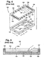
- the structure of a conventional pointing input device 100 will be hereinafter described with reference to Figs. 4 and 5.
- the pointing input device 100 has a case 101, a liquid crystal display panel 102, a transparent glass substrate 103 for protecting a surface of the liquid crystal display panel 102, and an optical touch panel 104 which are each laminated from underneath in the order described above.
- a liquid crystal driver (not shown) displays a plurality of kinds of pointing input information 105 on a display area of the liquid crystal display panel 102 in accordance with the application of pointing input. An operator carries out the pointing input as described later, with reference to the pointing input information 105.
- the optical touch panel 104 has light-emitting devices 108 arranged along the orthogonal X and Y directions of a rectangular frame 107 at equal intervals, and photoreceptor devices 109 arranged opposite to the light-emitting devices 108 and across the input operation area 107A of the rectangular frame 107.
- the light-emitting devices 108 sequentially emit light for scanning, and the photoreceptor devices 109 receive the light.
- the input operation area 107A enclosed within the rectangular frame 107 is disposed over the display area of the liquid crystal display panel 102, it is possible for the operator to carry out the pointing input, while looking at the pointing input information 105 displayed on the liquid crystal display panel 102 from above through the transparent glass substrate 103.
- the pointing input device 100 When the pointing input device 100 detects that the operator retracts the pen or the finger from the pointing input position of the input operation area 107A after detecting the pointing input, the pointing input device 100 outputs push detection data for carrying out a command in accordance with the pointing input position.
- pointing input information 105 are provided with pointing input areas 106 (shown in broken lines in the drawing) which are located above the pointing input information 105 in the input operation area 107A.
- the pointing input area 106 corresponds to a predetermined command indicated by the pointing input information 105.
- the predetermined command corresponding to the pointing input area 106 is carried out.
- the predetermined command corresponding to the pointing input information 105 is carried out.
- the conventional pointing input device 100 detects the pointing input to the input operation area 107A and the position thereof, and also when the operator releases the pointing input by retracting the pen or finger, the push detection data for carrying out the predetermined command is outputted. Therefore, the operator can change the pointing input position and enter the command corresponding to the specific pointing input position, while looking at the pointing input information 105.
- the push detection data is outputted every time the pointing input is released, in addition to when the pointing input is carried out by the operator inserting the pen or the finger into the pointing input area 106. Accordingly, there is a problem that the predetermined command can be carried out by mistake, such as when the operator retracts the pen or the finger from the pointing input area 106 for the purpose of simply finishing an operation.
- the pointing input device 100 always detects the pointing input even when the light beam is only momentarily intercepted. Thus, there is a problem that a water droplet, a bug, or the like passing through the input operation area 107A causes the pointing input device 100 to malfunction.
- WO 02/35460 discloses a touch confirming touch-screen, comprising a first sensor system for position coordinate determination and second sensor system for confirming each touch. The claims are delimited over this document.
- EP 0 372 964 A2 discloses a touch detection apparatus for an optical touch panel system, comprising touch detecting means for detecting a contact between a stylus and a display, and light emitting means together with light detecting means for an optical detection of position data of the stylus.
- US 5,231,381 discloses a data processing system with a touch-screen and a digitizing tablet, both integrated in an input device.
- an object of the present invention is to provide a pointing input device which sequentially outputs pointing position data indicating a pointing input position, and outputs push detection data in response to a pushing operation by using the same pen or finger for pointing input.
- Another object of the present invention is to provide a pointing input device in which a malfunction does not occur when a water droplet or a bug lands on an optical touch panel which is used for the detection of pointing input.
- the display area of the display panel is visible from the input operation area of the optical touch panel, so that an operator can carry out the pointing input by inserting a finger or the like in the input operation area, while looking at the pointing input information.
- the optical touch panel sequentially outputs the pointing position data indicating the detected pointing input position during the detection of the pointing input. Therefore, it is possible for the pointing input device to carry out a predetermined operation and to control the display in accordance with the pointing input position.
- the piezoelectric substrate When the transparent protective plate is pushed, the piezoelectric substrate outputs electric signals in response to the deformation of the transparent protective plate, and the push detection data is outputted. Therefore, it is possible to carry out the predetermined command at any pointing input position without releasing the pointing input.
- the push is detected by the piezoelectric substrate attached to the transparent protective plate, which protects the surface of the display panel against external force. Therefore, the pointing input device needs just a small space for attaching the piezoelectric substrate to detect the push, so that the whole pointing input device does not become large.
- the transparent protective plate is disposed under the input operation area, it is possible to push the transparent protective plate with the same finger or the like for the pointing input. Namely, the pointing input and the push operation can be continuously carried out.
- the pointing input device 1 is used as an input device for an ATM (automatic teller machine) installed in a bank, and the whole pointing input device 1 is installed so as to be flush with the surface of the ATM.
- ATM automated teller machine
- the pointing input device 1 has a plastic case 3 which contains a liquid crystal display panel 4, a transparent protective plate-5 for covering the surface of the liquid crystal display panel 4, a pair of piezoelectric substrates 6A and 6B (See Fig.3) attached along the two edges, which are perpendicular to each other, of the transparent protective plate 5, and an optical touch panel 9 provided with plural pairs of light-emitting devices 7 and photoreceptor devices 8.
- the case 3 in the shape of a rectangular parallelepiped, is installed so as to be flush with the surface of the main body 2 of the ATM, as an operation surface.
- the case 3 is, as shown in Fig. 2, secured with screws 10 which penetrate flanges 3a from the inside of the main body 2.
- a rectangular shaped opening formed in the top plate of the case 3 serves as the input operation area 9A of the optical touch panel 9.
- the liquid crystal display panel 4 and the transparent protective plate 5 are so contained inside the case 3 that the display area of the liquid crystal display panel 4 can be seen from the input operation area 9A through the transparent protective plate 5.
- the liquid crystal display panel 4, the piezoelectric substrates 6A and 6B, and the optical touch panel 9 are connected to each circuit component shown in Fig. 3 with cables (not illustrated) drawn out of the case 3.
- the liquid crystal display panel 4 displays any pointing input information 11 for carrying out pointing input at any position of the display area, in response to control from a liquid crystal driver (not illustrated).
- the pointing input device 1 is used in the ATM of the bank, as shown in Fig. 1, the pointing input information 11 about how to operate, about a deposit and withdrawal, and the like is displayed as an initial screen.
- the pointing input information 11 is displayed as a message to the operator in the form of text, numbers, or the like.
- a backlight panel (not illustrated) is disposed between the rear surface of the liquid crystal display panel 4 and the case 3.
- a reflective film is glued on the rear surface of the backlight panel.
- the backlight panel disperses light from a backlight source and illuminates the liquid crystal display panel 4 from its backside, for the purpose of making it easy for an operator to look at the pointing input information 11.
- the transparent protective panel 5 is laminated on the surface of the liquid crystal display panel 4 via a pressure-sensitive adhesive sheet 12 so as to cover the surface of the liquid crystal display panel 4. Being attached to the surface of the liquid crystal display panel 4 with the pressure-sensitive adhesive sheet 12, the transparent protective plate 5 freely deforms without any constraint, so that it is possible to detect a push in response to the deformation of the transparent protective plate 5, as described later.
- Each of the piezoelectric substrates 6A and 6B is a single-layer substrate made of piezoelectric material such as piezoelectric ceramic which is typified by piezoelectric single crystal and PZT (lead zirconate titanate), polyvinylidene fluoride (PVDF), and the like.
- the piezoelectric substrates 6A and 6B of this embodiment are composed of piezoelectric ceramic plates made of the piezoelectric ceramic material of a PZT series, which has mechanical durability and is most widely used.
- the piezoelectric substrates 6A and 6B are formed in the shape of elongated and thin plates along the edges of the transparent protective plate 5 along X and Y directions, orthogonal to each other.
- each of the piezoelectric substrates 6A and 6B is the thin plate with a single-layer, and the height thereof is approximately 200 ⁇ m even when the height of a leading electrode secured on the surface thereof is included. Because the piezoelectric substrates 6A and 6B are not bulky, it is possible to attach the piezoelectric substrates 6A and 6B to any of the positions of the ordinary transparent protective plate 5 without considering space for installation.
- This invention takes advantage of the piezoelectric effect of the piezoelectric substrates 6A and 6B (i.e., takes advantage of voltage signals generated by mechanical deformation).
- the piezoelectric substrates 6A and 6B are attached to the transparent protective plate 5 along the edges thereof by applying various kinds of adhesives like an epoxy adhesive, an acrylic adhesive, and the like.
- the transparent protective plate 5 when the transparent protective plate 5 is pushed, the deformation is transmitted to the piezoelectric substrates 6A and 6B, and voltage is outputted in response to the deformation of the piezoelectric substrates 6A and 6B.
- the piezoelectric substrates 6A and 6B do not cover the display area because they are attached to the edges of the transparent protective plate 5. Also, the piezoelectric substrates 6A and 6B cannot be seen from the outside, because they are contained in the case 3 enclosing the input operation area 9A. However, the piezoelectric substrates 6A and 6B can be attached anywhere, as long as the piezoelectric substrates 6A and 6B can detect the deformation of the transparent protective plate 5.
- the optical touch panel 9 is provided with a number of light-emitting devices 7 and photoreceptor devices 8 arranged along the periphery of the opening of the case 3 (the input operation area 9A), for the purpose of detecting the pointing input with a finger, a pen or the like, and the pointing input position.
- the light-emitting devices 7 are arranged at equal intervals along the orthogonal X and Y directions of the periphery of the input operation area 9A and are positioned facing inward toward the center of the input operation area 9A.
- the photoreceptor devices 8, in pairs with the light-emitting devices 7, are arranged inside the case 3 opposite to the corresponding light-emitting devices 7 across the input-operation area 9A.
- the light-emitting devices 7 arranged in this manner sequentially emit light for scanning, reticulate scanning light paths, as shown in dashed lines in Fig. 1, are formed in the input operation area 9A.
- the pen or the finger intercepts light beams which pass through the pointing input position in the X and Y directions.
- the photoreceptor devices 8 placed in the light paths do not receive the light beams from the corresponding light-emitting devices 7 with proper timing to the light emission of the light-emitting devices 7. Therefore, it is possible to detect the pointing input by the operator and X and Y coordinates which indicate the pointing input position.
- pointing input areas 13 are virtually provided in the input operation area 9A. Each of the pointing input areas 13 corresponds to the predetermined command for the ATM.
- the pointing input areas 13 are provided in the input operation area 9A, above the display positions of the pointing input information 11.
- the pointing input area 13 is divided off from a surrounding area with a rectangular outline indicated by X and Y coordinates.
- the operator can carry out the pointing input to the pointing input area 13 corresponding to the pointing input information 11 by means of inserting the finger or the pen in the input operation area 9A, and by looking at the pointing input information 11 displayed on the liquid crystal display panel 4 from above through the transparent protective plate 5.
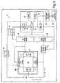
- Fig. 3 is a block diagram of circuit components provided in the pointing input device 1 for the purpose of judging the push as described above, and detecting the pointing input and the pointing input position. The operation of the pointing input device 1 will be hereinafter described with reference to Fig.3.
- the plural light-emitting devices 7 (corresponding to LED X Axis and LED Y Axis shown in Fig. 3), which are arranged along the X and Y directions of the input operation area 9A, are connected to a constant current circuit 14.
- Each of the light-emitting devices 7 is composed of an LED which emits a light beam in response to a flow of constant current.
- Each light-emitting device 7 is connected to an LED multiplexer 16 via the constant current circuit 14.
- a CPU 15 controls the connection between each light-emitting device 7 and the LED multiplexer 16.
- the constant current circuit 14 is connected to the CPU 15 via a digital-to-analog converter 17.
- the CPU 15 applies driving current to each light-emitting device 7 with predetermined scanning timing in order of arrangement position, for the purpose of emitting the light beam.
- plural photoreceptor devices 8, arranged opposite to each of the plural light-emitting devices 7 across the input operation area 9A, are composed of phototransistors which receive the light beam and output light-reception signals.
- Each of the photoreceptor devices 8 is connected to a Ptr multiplexer 18 by which the CPU 15 controls a connection between the individual photoreceptor device 8 and an integrator circuit 19.
- the CPU 15 connects the photoreceptor device 8, opposite to the light-emitting device 7 to which the driving current is applied so as to be controlled, to the integrator circuit 19, in synchronization with the light emission control.
- the output from the integrator circuit 19 is inputted to the CPU 15 via an analog-to-digital converter 25, so that the CPU 15 can obtain the integrated light-reception signals from the integrator circuit 19 with the scanning timing of each light-emitting device 7, unless the light beam is intercepted within the input operation area 9A, in other words, there is the pointing input.
- the CPU 15 detects the pointing input by the operator and the X and Y coordinates indicating the pointing input position, by means of stopping the light-reception signals to be inputted and its timing.
- Each of the piezoelectric substrates 6A and 6B attached to the edges of the transparent protective plate 5 is connected to the input of the CPU 15 via an amplifier circuit 20.
- the deformation is transmitted to the piezoelectric substrates 6A and 6B.
- the voltage signals generated in response to the deformation of the piezoelectric substrates 6A and 6B is amplified by the amplifier circuit 20 and then inputted to the CPU 15.
- the threshold voltage is set at a voltage level which is equal to a voltage outputted from the amplifier circuit 20 when the operator consciously pushes the transparent protective plate 5 with a force that is greater than a predetermined pushing force, so that the CPU 15 does not judge the push if the operator unconsciously touches the transparent protective plate 5.
- the piezoelectric substrates 6A and 6B are attached to the edges of the transparent protective plate 5 along the X and Y directions, which are orthogonal to each other. Accordingly, if the operator pushes any position in the transparent protective plate 5, the deformation is transmitted to any of the piezoelectric substrates 6A and 6B and the push is judged.
- the output of the CPU 15 is connected to a host computer 22 via an input-output interface 21.
- the CPU 15 outputs pointing position data indicating the pointing input position via the input-output interface 21 while detecting the pointing input. In a case where the push is judged, the CPU 15 outputs push detection data together with the pointing position data.
- a ROM 23 and a RAM 24 connected to the CPU 15 are memory devices for storing a program to carry out the above operation of the CPU 15, for storing the threshold voltage for judging the push and the like, and for temporarily storing inputted data.
- the host computer 22 outputs predetermined display control signals to the liquid crystal driver (not illustrated) in order to control the display of the liquid crystal display panel 4, and makes the ATM carry out the predetermined commands.
- a cursor appears in the display area corresponding to the pointing input position of the liquid crystal display panel 4, in order to inform the operator of the detection of the pointing input and the pointing input position.
- the host computer 22 constantly judges whether or not the pointing input position indicated by the pointing position data is within any of the pointing input areas 13, as long as the pointing position data is inputted. When the pointing input position is within the specific pointing input area 13, and also the push detection data is inputted, the host computer 22 makes the ATM carry out the predetermined command corresponding to the pointing input area 13.
- the push detection data is outputted to the host computer 22.
- the host computer 22 makes the ATM carry out an operation for the "deposit,” such as displaying the pointing input information 11 for inputting an amount of money deposited on the liquid crystal display panel 4, controlling an opening of a shutter for depositing bills, and the like.
- the host computer 22 carrying out the above operation may be disposed inside the pointing input device 1.
- the CPU 15 may carry out the operation as the host computer 22.
- the pointing position data and the push detection data are outputted and the predetermined command is carried out.
- the CPU 15 may not output the pointing position data constantly even if the push is detected, but the pointing position data may be outputted when the push is judged.
- the pointing input device of the present invention even if a bug, a water droplet, or the like, which passes through the input operation area 9A, temporarily intercepts the light beams, the pointing position data indicating the intercepted position is not outputted by mistake. Therefore, it is possible for the operator to certainly carry out the pointing input with the intentional pushing operation.
- the display panel is the liquid crystal display panel 4 in this embodiment.
- the display panel may be a CRT, a plasma display panel, or the like, as long as the display panel can display various kinds of pointing input information at any position on a plane.
- One pair of the piezoelectric substrates are attached to the transparent protective plate 5 in this embodiment, but one piezoelectric substrate or three or more divided piezoelectric substrates may be used, as long as the piezoelectric substrate(s) can detect the deformation by the push.
- the integrator circuit is provided between the outputs of the piezoelectric substrates and the CPU 15, electric signals indicating the amplitude of the deformation in accordance with the strength of the push are inputted to the CPU 15.
- the CPU 15 can output the strength data of the push against the transparent protective plate 5.
- both the pointing position data indicating the pointing input position and the push detection data representing the push against the transparent protective plate are outputted together.
- the operator can output data corresponding to the pushing operation while moving a mouse.
- the push can be detected by the pointing input device with simple structure in which the piezoelectric substrates are only attached to the transparent protective plate, which protects the display area of the display panel. Therefore, there are advantages that the pointing input device does not become large, and existing parts can be used therein.
- the pointing input data is outputted.
- the pointing position data is not outputted, so that it is possible to prevent a malfunction of the pointing input device.
- the push can be detected by the pointing input device with the simple structure in which the piezoelectric substrates are only attached to the transparent protective plate, which protects the display area of the display panel. Therefore, it is possible to use the structure of the conventional pointing input device as-is.
- one pair of the piezoelectric substrates is attached to the transparent protective plate and the piezoelectric substrates are orthogonal to each other.
- the transparent protective plate deforms in any direction in response to the push, the deformation is transmitted to any of the piezoelectric substrates, so that the push is certainly detected.
Claims (5)
- Zeigeeingabevorrichtung (1), umfassend:ein Anzeigefeld (4), ausgeführt zum Anzeigen von Informationen auf einem Anzeigebereich (13, 106);eine transparente Schutzplatte (5), welche auf den Anzeigebereich (13, 106) des Anzeigefelds (4) laminiert ist;ein piezoelektrisches Substrat (6A, 6B), welches an der transparenten Schutzplatte (5) befestigt ist und so ausgeführt ist, dass es eine Verformung, die durch ein Drücken gegen die transparente Schutzplatte (5) verursacht wird, in ein elektrisches Signal umwandelt, und ferner so ausgeführt ist, dass es das elektrische Signal ausgibt; undein optisches Berührungsfeld (9), welches sich auf der transparenten Schutzplatte (5) befindet und so ausgeführt ist, dass es Lichtstrahlen aussendet, um einen Eingabe-Bedienbereich (9A) des optischen Berührungsfeldes (9) entlang den orthogonalen X- und Y-Richtungen netzartig abzutasten, um eine Zeigeeingabe und eine Zeigeeingabeposition im Eingabe-Bedienbereich (9A) zu erfassen, wenn die Lichtstrahlen durch die Zeigeeingabe unterbrochen werden, wobei der Eingabe-Bedienbereich (9A) den Anzeigebereich (13, 106) überlagert, welcher durch die transparente Schutzplatte (5) hindurch sichtbar ist, dadurch gekennzeichnet, dassdie Zeigeeingabevorrichtung (1) so ausgeführt ist, dass sie Drückerfassungsdaten zusammen mit Zeigepositionsdaten, welche die Zeigeeingabeposition anzeigen, nur ausgibt, wenn das elektrische Signal aus dem piezoelektrischen Substrat (6A, 6B) ausgegeben wird und das Drücken gegen die transparente Schutzplatte (5) bestätigt wird, während das optische Berührungsfeld (9) die Zeigeeingabe erfasst, wodurch eine Aktivierung der Zeigeeingabevorrichtung angezeigt wird; und dadurch gekennzeichnet, dass die Zeigeeingabevorrichtung (1) ferner so ausgeführt ist, dass sie die Zeigepositionsdaten erfasst und ausgibt, während das optische Berührungsfeld (9) die Zeigeeingabe erfasst und während das piezoelektrische Substrat (6A, 6B) kein elektrisches Signal ausgibt, welches ein Drücken gegen die transparente Schutzplatte (5) anzeigt.
- Zeigeeingabevorrichtung nach Anspruch 1, wobei das piezoelektrische Substrat ein Paar piezoelektrischer Substrate schmaler und lang gestreckter Form umfasst, und die piezoelektrischen Substrate an der transparenten Schutzplatte befestigt und orthogonal zueinander sind.
- Zeigeeingabevorrichtung nach Anspruch 1 oder 2, wobei die Drückerfassungsdaten und die Zeigepositionsdaten nur zusammen ausgegeben werden, wenn das optische Berührungsfeld die Zeigeeingabe erfasst und das piezoelektrische Substrat die Drückerfassungsdaten erfasst.
- Zeigeeingabevorrichtung nach Anspruch 1 oder 2, weiterhin umfassend:eine Steuereinheit, welche so ausgeführt ist, dass sie ermittelt, ob das piezoelektrische Substrat das elektrische Signal ausgegeben hat, das ein Drücken gegen die transparente Schutzplatte anzeigt, um zu ermitteln, ob das Drücken gegen die transparente Schutzplatte stattgefunden hat, während das optische Berührungsfeld die Zeigeeingabe erfasst, und um Drückerfassungsdaten zusammen mit den Zeigepositionsdaten nur auszugeben, wenn die Steuereinheit ermittelt hat, dass das elektrische Signal während der Erfassung der Zeigeeingabe vorliegt.
- Zeigeeingabevorrichtung nach einem der Ansprüche 1 bis 4, wobei die Zeigeeingabevorrichtung Zeigepositionsdaten ausgibt, die von dem optischen Berührungsfeld erfasst werden, wenn die Steuereinheit ermittelt, dass das von dem piezoelektrischen Substrat ausgegebene elektrische Signal größer oder gleich einer vorgegebenen Schwellenspannung ist, das Drücken gegen die transparente Schutzplatte mit einer größeren als einer vorgegebenen Drückkraft geschieht und das Drücken gegen die transparente Schutzplatte geschieht, während das optische Berührungsfeld die Zeigeeingabe erfasst.
Applications Claiming Priority (2)
| Application Number | Priority Date | Filing Date | Title |
|---|---|---|---|
| JP2002292207 | 2002-10-04 | ||
| JP2002292207A JP2004127073A (ja) | 2002-10-04 | 2002-10-04 | 指示入力装置 |
Publications (3)
| Publication Number | Publication Date |
|---|---|
| EP1408396A2 EP1408396A2 (de) | 2004-04-14 |
| EP1408396A3 EP1408396A3 (de) | 2005-02-02 |
| EP1408396B1 true EP1408396B1 (de) | 2007-12-12 |
Family
ID=32025461
Family Applications (1)
| Application Number | Title | Priority Date | Filing Date |
|---|---|---|---|
| EP03021149A Expired - Fee Related EP1408396B1 (de) | 2002-10-04 | 2003-09-22 | Eingabegerät mit Hinweisvorrichtung |
Country Status (7)
| Country | Link |
|---|---|
| US (1) | US7199788B2 (de) |
| EP (1) | EP1408396B1 (de) |
| JP (1) | JP2004127073A (de) |
| KR (1) | KR20040031562A (de) |
| CN (1) | CN1487403A (de) |
| DE (1) | DE60317988T2 (de) |
| TW (1) | TW200405977A (de) |
Families Citing this family (30)
| Publication number | Priority date | Publication date | Assignee | Title |
|---|---|---|---|---|
| US7834855B2 (en) | 2004-08-25 | 2010-11-16 | Apple Inc. | Wide touchpad on a portable computer |
| US8339379B2 (en) * | 2004-04-29 | 2012-12-25 | Neonode Inc. | Light-based touch screen |
| JP4279207B2 (ja) * | 2004-06-18 | 2009-06-17 | アルプス電気株式会社 | 入力装置およびこの入力装置を用いた表示入力装置 |
| US7825902B2 (en) * | 2005-03-31 | 2010-11-02 | Avego Technologies General Ip (Singapore) Pte. Ltd. | Controller, system and method for identifying a number of interactions with a computer input area |
| US8552986B2 (en) * | 2005-08-31 | 2013-10-08 | Avago Technologies General Ip (Singapore) Pte. Ltd. | Scalable controller for a computer input area |
| CN101000529B (zh) * | 2006-01-13 | 2011-09-14 | 北京汇冠新技术股份有限公司 | 一种用于红外触摸屏的触摸力检测装置 |
| JP4687478B2 (ja) * | 2006-01-31 | 2011-05-25 | ぺんてる株式会社 | 静電容量型タッチスイッチ装置 |
| KR101357496B1 (ko) * | 2006-07-05 | 2014-02-03 | 엘지전자 주식회사 | 냉장고의 입력장치 |
| KR101303881B1 (ko) * | 2006-08-03 | 2013-09-04 | 삼성디스플레이 주식회사 | 터치 스크린, 그 제조 방법 및 이를 구비하는 표시 장치 |
| JP4775247B2 (ja) * | 2006-12-21 | 2011-09-21 | 三菱電機株式会社 | 位置検出装置 |
| KR100868824B1 (ko) | 2007-04-30 | 2008-11-14 | 안영수 | 광학방식 터치스크린 |
| TWI346890B (en) * | 2007-05-16 | 2011-08-11 | Hannstar Display Corp | Light pointing device employed in input apparatus, driving method thereof, and lcd using the same |
| US8619039B2 (en) * | 2007-12-21 | 2013-12-31 | Motorola Mobility Llc | Translucent touch screen devices including low resistive mesh |
| US20090174679A1 (en) | 2008-01-04 | 2009-07-09 | Wayne Carl Westerman | Selective Rejection of Touch Contacts in an Edge Region of a Touch Surface |
| JP2009301250A (ja) * | 2008-06-12 | 2009-12-24 | Smk Corp | 入力装置の複数指示位置の制御装置、その方法及びその記録媒体 |
| TWI409674B (zh) * | 2008-11-25 | 2013-09-21 | Bruce C S Chou | 具多輸入訊息之微型觸控裝置 |
| US8294047B2 (en) | 2008-12-08 | 2012-10-23 | Apple Inc. | Selective input signal rejection and modification |
| TWI376624B (en) * | 2008-12-23 | 2012-11-11 | Integrated Digital Tech Inc | Force-sensing modules for light sensitive screens |
| DE102009003990A1 (de) * | 2009-01-07 | 2010-07-08 | Wincor Nixdorf International Gmbh | Berührungssensitive Eingabevorrichtung |
| US8913034B2 (en) | 2009-05-25 | 2014-12-16 | Pixart Imaging Inc. | Connector of connecting light sensor and substrate and method of fabricating light sensor |
| TWI385880B (zh) * | 2009-05-25 | 2013-02-11 | Pixart Imaging Inc | 連接光感測器與基板之連接器與光感測器之製作方法 |
| KR20110009973A (ko) * | 2009-07-23 | 2011-01-31 | 삼성전자주식회사 | 디스플레이 시스템 및 디스플레이 시스템의 제어 방법 |
| JP2011034380A (ja) * | 2009-08-03 | 2011-02-17 | Nitto Denko Corp | タッチパネルおよびタッチパネル付表示装置 |
| KR101352117B1 (ko) * | 2009-10-22 | 2014-01-14 | 엘지디스플레이 주식회사 | 터치 패널을 갖는 표시 장치 및 이의 터치 감지 방법 |
| JP4838369B2 (ja) * | 2010-03-30 | 2011-12-14 | Smk株式会社 | タッチパネルの入力位置出力方法 |
| JP2012053840A (ja) * | 2010-09-03 | 2012-03-15 | Toshiba Tec Corp | 光学式タッチデバイス |
| KR101159179B1 (ko) * | 2010-10-13 | 2012-06-22 | 액츠 주식회사 | 터치 스크린 시스템 및 그 제조 방법 |
| JP5597583B2 (ja) * | 2011-03-28 | 2014-10-01 | 太陽誘電株式会社 | タッチパネル装置及び電子機器 |
| FR2989829B1 (fr) * | 2012-04-20 | 2014-04-11 | Commissariat Energie Atomique | Capteur tactile photosensible |
| TWI582671B (zh) * | 2012-11-15 | 2017-05-11 | 緯創資通股份有限公司 | 光學式觸控裝置和其觸控方法 |
Family Cites Families (30)
| Publication number | Priority date | Publication date | Assignee | Title |
|---|---|---|---|---|
| IL74979A (en) | 1984-05-18 | 1991-08-16 | Hughes Aircraft Co | Precision display position designation system using coarse touch panel input |
| US4698460A (en) * | 1986-08-26 | 1987-10-06 | Tektronix, Inc. | Touch panel system |
| US4698461A (en) * | 1986-08-26 | 1987-10-06 | Tektronix, Inc. | Touch panel with automatic frequency control |
| US4707845A (en) * | 1986-08-26 | 1987-11-17 | Tektronix, Inc. | Touch panel with automatic nulling |
| US5117146A (en) * | 1988-04-29 | 1992-05-26 | The United States Of America As Represented By The United States Department Of Energy | Acoustic wave device using plate modes with surface-parallel displacement |
| EP0372964A3 (de) | 1988-12-08 | 1990-12-27 | Tektronix Inc. | Berührungsdetektionsvorrichtung für ein optisches Berührungsanzeigesystem |
| US5305017A (en) * | 1989-08-16 | 1994-04-19 | Gerpheide George E | Methods and apparatus for data input |
| DE68928987T2 (de) | 1989-10-02 | 1999-11-11 | Koninkl Philips Electronics Nv | Datenverarbeitungssystem mit einer Berührungsanzeige und einem Digitalisiertablett, beide integriert in einer Eingabevorrichtung |
| US5573077A (en) * | 1990-11-16 | 1996-11-12 | Knowles; Terence J. | Acoustic touch position sensor |
| GB2263765A (en) | 1992-01-25 | 1993-08-04 | Paul Philip Oliver | Touch screen systems |
| US5673066A (en) * | 1992-04-21 | 1997-09-30 | Alps Electric Co., Ltd. | Coordinate input device |
| US5355149A (en) | 1992-05-27 | 1994-10-11 | Spacelabs Medical, Inc. | Scanning system for touch screen keyboards |
| US5861875A (en) * | 1992-07-13 | 1999-01-19 | Cirque Corporation | Methods and apparatus for data input |
| US5897648A (en) | 1994-06-27 | 1999-04-27 | Numonics Corporation | Apparatus and method for editing electronic documents |
| US5591945A (en) * | 1995-04-19 | 1997-01-07 | Elo Touchsystems, Inc. | Acoustic touch position sensor using higher order horizontally polarized shear wave propagation |
| WO1998029853A1 (en) * | 1996-12-25 | 1998-07-09 | Elo Touchsystems, Inc. | Grating transducer for acoustic touchscreen |
| JPH1186698A (ja) * | 1997-09-11 | 1999-03-30 | J R Higashi Nippon Mechatronics Kk | 光学式タッチパネル |
| US6104374A (en) * | 1998-02-19 | 2000-08-15 | Tektronix, Inc. | Sparse vector rasterization |
| US6110565A (en) * | 1998-04-27 | 2000-08-29 | Matthews; James A. | Heat bond seaming tape and method of manufacture |
| US6111565A (en) | 1998-05-14 | 2000-08-29 | Virtual Ink Corp. | Stylus for use with transcription system |
| US6731270B2 (en) * | 1998-10-21 | 2004-05-04 | Luidia Inc. | Piezoelectric transducer for data entry device |
| JP2000347807A (ja) | 1999-06-08 | 2000-12-15 | Newcom:Kk | 指やペンなどにより入力可能な座標入力装置 |
| US6504530B1 (en) * | 1999-09-07 | 2003-01-07 | Elo Touchsystems, Inc. | Touch confirming touchscreen utilizing plural touch sensors |
| US6492979B1 (en) * | 1999-09-07 | 2002-12-10 | Elo Touchsystems, Inc. | Dual sensor touchscreen utilizing projective-capacitive and force touch sensors |
| AU2001212430A1 (en) | 2000-10-27 | 2002-05-06 | Elo Touchsystems, Inc. | Touch confirming touchscreen utilizing plural touch sensors |
| US6784871B2 (en) * | 2001-07-26 | 2004-08-31 | Kohji Toda | Ultrasonic security system for personal computer |
| JP3798287B2 (ja) * | 2001-10-10 | 2006-07-19 | Smk株式会社 | タッチパネル入力装置 |
| US7337410B2 (en) * | 2002-11-06 | 2008-02-26 | Julius Lin | Virtual workstation |
| US7098574B2 (en) * | 2002-11-08 | 2006-08-29 | Toyo Communication Equipment Co., Ltd. | Piezoelectric resonator and method for manufacturing the same |
| US20040263484A1 (en) * | 2003-06-25 | 2004-12-30 | Tapio Mantysalo | Multifunctional UI input device for moblie terminals |
-
2002
- 2002-10-04 JP JP2002292207A patent/JP2004127073A/ja active Pending
-
2003
- 2003-02-24 KR KR1020030011262A patent/KR20040031562A/ko not_active Application Discontinuation
- 2003-06-10 TW TW092115729A patent/TW200405977A/zh unknown
- 2003-06-27 CN CNA031452884A patent/CN1487403A/zh active Pending
- 2003-07-17 US US10/622,268 patent/US7199788B2/en not_active Expired - Fee Related
- 2003-09-22 DE DE60317988T patent/DE60317988T2/de not_active Expired - Lifetime
- 2003-09-22 EP EP03021149A patent/EP1408396B1/de not_active Expired - Fee Related
Also Published As
| Publication number | Publication date |
|---|---|
| US20040066379A1 (en) | 2004-04-08 |
| US7199788B2 (en) | 2007-04-03 |
| CN1487403A (zh) | 2004-04-07 |
| JP2004127073A (ja) | 2004-04-22 |
| EP1408396A2 (de) | 2004-04-14 |
| DE60317988T2 (de) | 2008-12-18 |
| EP1408396A3 (de) | 2005-02-02 |
| DE60317988D1 (de) | 2008-01-24 |
| KR20040031562A (ko) | 2004-04-13 |
| TW200405977A (en) | 2004-04-16 |
Similar Documents
| Publication | Publication Date | Title |
|---|---|---|
| EP1408396B1 (de) | Eingabegerät mit Hinweisvorrichtung | |
| TW556108B (en) | Coordinate input device detecting touch on board associated with liquid crystal display, and electronic device therefor | |
| KR100837738B1 (ko) | 전자 장치 및 이 장치의 터치패널 배치 방법 | |
| US8125454B2 (en) | Resistive type touch panel | |
| US10055062B2 (en) | Pressure sensing display | |
| EP1847914A1 (de) | Informationseingabeeinrichtung | |
| KR20170079884A (ko) | 표시 장치 | |
| CN109074192B (zh) | 压力感测显示器 | |
| US20100207910A1 (en) | Optical Sensing Screen and Panel Sensing Method | |
| KR20060123182A (ko) | 촉각식 접촉 감지 시스템 | |
| EP2428881A2 (de) | Eingabevorrichtung für ein mobiltelefon | |
| US20060164387A1 (en) | Input apparatus and touch-reading character/symbol input method | |
| KR20080100008A (ko) | 멀티 터치 장치 | |
| US10345964B2 (en) | Display panel and display device | |
| KR20180019891A (ko) | 액티브 스타일러스 펜, 이를 갖는 터치 센싱 시스템 및 이를 이용한 터치 센싱 방법 | |
| KR102524430B1 (ko) | 표시장치 | |
| US10725545B2 (en) | Touch panel with tactile force feedback, tactile force feedback system thereof, and display device | |
| JP3273384B2 (ja) | 座標入力装置 | |
| KR20050077230A (ko) | 펜 형의 위치 입력 장치 | |
| US20130170185A1 (en) | Display device with optical recognition of inputting instrument | |
| US11921962B2 (en) | Sensor module and touch panel with first sensor array to detect non-contact touch and second sensor array to detect contacting touch | |
| US11681375B1 (en) | Non-uniform pressure actuation threshold value | |
| WO2022190724A1 (ja) | センサモジュール及びそれを備えたタッチパネル | |
| JPS6154525A (ja) | タツチパネル入力装置 | |
| KR20190030362A (ko) | 터치센서 및 그를 포함하는 표시장치 |
Legal Events
| Date | Code | Title | Description |
|---|---|---|---|
| PUAI | Public reference made under article 153(3) epc to a published international application that has entered the european phase |
Free format text: ORIGINAL CODE: 0009012 |
|
| AK | Designated contracting states |
Kind code of ref document: A2 Designated state(s): AT BE BG CH CY CZ DE DK EE ES FI FR GB GR HU IE IT LI LU MC NL PT RO SE SI SK TR |
|
| AX | Request for extension of the european patent |
Extension state: AL LT LV MK |
|
| PUAL | Search report despatched |
Free format text: ORIGINAL CODE: 0009013 |
|
| AK | Designated contracting states |
Kind code of ref document: A3 Designated state(s): AT BE BG CH CY CZ DE DK EE ES FI FR GB GR HU IE IT LI LU MC NL PT RO SE SI SK TR |
|
| AX | Request for extension of the european patent |
Extension state: AL LT LV MK |
|
| RIC1 | Information provided on ipc code assigned before grant |
Ipc: 7G 06K 11/00 A Ipc: 7G 06F 3/033 B |
|
| 17P | Request for examination filed |
Effective date: 20050513 |
|
| 17Q | First examination report despatched |
Effective date: 20050617 |
|
| AKX | Designation fees paid |
Designated state(s): DE FR GB |
|
| R17C | First examination report despatched (corrected) |
Effective date: 20050617 |
|
| GRAP | Despatch of communication of intention to grant a patent |
Free format text: ORIGINAL CODE: EPIDOSNIGR1 |
|
| GRAS | Grant fee paid |
Free format text: ORIGINAL CODE: EPIDOSNIGR3 |
|
| GRAA | (expected) grant |
Free format text: ORIGINAL CODE: 0009210 |
|
| AK | Designated contracting states |
Kind code of ref document: B1 Designated state(s): DE FR GB |
|
| REG | Reference to a national code |
Ref country code: GB Ref legal event code: FG4D |
|
| REF | Corresponds to: |
Ref document number: 60317988 Country of ref document: DE Date of ref document: 20080124 Kind code of ref document: P |
|
| ET | Fr: translation filed | ||
| PLBE | No opposition filed within time limit |
Free format text: ORIGINAL CODE: 0009261 |
|
| STAA | Information on the status of an ep patent application or granted ep patent |
Free format text: STATUS: NO OPPOSITION FILED WITHIN TIME LIMIT |
|
| 26N | No opposition filed |
Effective date: 20080915 |
|
| PGFP | Annual fee paid to national office [announced via postgrant information from national office to epo] |
Ref country code: DE Payment date: 20140922 Year of fee payment: 12 |
|
| PGFP | Annual fee paid to national office [announced via postgrant information from national office to epo] |
Ref country code: FR Payment date: 20140919 Year of fee payment: 12 Ref country code: GB Payment date: 20140919 Year of fee payment: 12 |
|
| REG | Reference to a national code |
Ref country code: DE Ref legal event code: R119 Ref document number: 60317988 Country of ref document: DE |
|
| GBPC | Gb: european patent ceased through non-payment of renewal fee |
Effective date: 20150922 |
|
| REG | Reference to a national code |
Ref country code: FR Ref legal event code: ST Effective date: 20160531 |
|
| PG25 | Lapsed in a contracting state [announced via postgrant information from national office to epo] |
Ref country code: DE Free format text: LAPSE BECAUSE OF NON-PAYMENT OF DUE FEES Effective date: 20160401 Ref country code: GB Free format text: LAPSE BECAUSE OF NON-PAYMENT OF DUE FEES Effective date: 20150922 |
|
| PG25 | Lapsed in a contracting state [announced via postgrant information from national office to epo] |
Ref country code: FR Free format text: LAPSE BECAUSE OF NON-PAYMENT OF DUE FEES Effective date: 20150930 |