EP1403691A1 - Electro-optical display device and its manufacturing method including the transfer of a chip - Google Patents
Electro-optical display device and its manufacturing method including the transfer of a chip Download PDFInfo
- Publication number
- EP1403691A1 EP1403691A1 EP20030255715 EP03255715A EP1403691A1 EP 1403691 A1 EP1403691 A1 EP 1403691A1 EP 20030255715 EP20030255715 EP 20030255715 EP 03255715 A EP03255715 A EP 03255715A EP 1403691 A1 EP1403691 A1 EP 1403691A1
- Authority
- EP
- European Patent Office
- Prior art keywords
- basic
- substrate
- chip
- electro
- chips
- Prior art date
- Legal status (The legal status is an assumption and is not a legal conclusion. Google has not performed a legal analysis and makes no representation as to the accuracy of the status listed.)
- Granted
Links
Images




Classifications
-
- H—ELECTRICITY
- H05—ELECTRIC TECHNIQUES NOT OTHERWISE PROVIDED FOR
- H05B—ELECTRIC HEATING; ELECTRIC LIGHT SOURCES NOT OTHERWISE PROVIDED FOR; CIRCUIT ARRANGEMENTS FOR ELECTRIC LIGHT SOURCES, IN GENERAL
- H05B33/00—Electroluminescent light sources
- H05B33/12—Light sources with substantially two-dimensional [2D] radiating surfaces
- H05B33/26—Light sources with substantially two-dimensional [2D] radiating surfaces characterised by the composition or arrangement of the conductive material used as an electrode
-
- H—ELECTRICITY
- H10—SEMICONDUCTOR DEVICES; ELECTRIC SOLID-STATE DEVICES NOT OTHERWISE PROVIDED FOR
- H10D—INORGANIC ELECTRIC SEMICONDUCTOR DEVICES
- H10D86/00—Integrated devices formed in or on insulating or conducting substrates, e.g. formed in silicon-on-insulator [SOI] substrates or on stainless steel or glass substrates
-
- G—PHYSICS
- G02—OPTICS
- G02F—OPTICAL DEVICES OR ARRANGEMENTS FOR THE CONTROL OF LIGHT BY MODIFICATION OF THE OPTICAL PROPERTIES OF THE MEDIA OF THE ELEMENTS INVOLVED THEREIN; NON-LINEAR OPTICS; FREQUENCY-CHANGING OF LIGHT; OPTICAL LOGIC ELEMENTS; OPTICAL ANALOGUE/DIGITAL CONVERTERS
- G02F1/00—Devices or arrangements for the control of the intensity, colour, phase, polarisation or direction of light arriving from an independent light source, e.g. switching, gating or modulating; Non-linear optics
- G02F1/01—Devices or arrangements for the control of the intensity, colour, phase, polarisation or direction of light arriving from an independent light source, e.g. switching, gating or modulating; Non-linear optics for the control of the intensity, phase, polarisation or colour
- G02F1/13—Devices or arrangements for the control of the intensity, colour, phase, polarisation or direction of light arriving from an independent light source, e.g. switching, gating or modulating; Non-linear optics for the control of the intensity, phase, polarisation or colour based on liquid crystals, e.g. single liquid crystal display cells
- G02F1/133—Constructional arrangements; Operation of liquid crystal cells; Circuit arrangements
- G02F1/136—Liquid crystal cells structurally associated with a semi-conducting layer or substrate, e.g. cells forming part of an integrated circuit
- G02F1/1362—Active matrix addressed cells
- G02F1/13624—Active matrix addressed cells having more than one switching element per pixel
-
- H—ELECTRICITY
- H10—SEMICONDUCTOR DEVICES; ELECTRIC SOLID-STATE DEVICES NOT OTHERWISE PROVIDED FOR
- H10W—GENERIC PACKAGES, INTERCONNECTIONS, CONNECTORS OR OTHER CONSTRUCTIONAL DETAILS OF DEVICES COVERED BY CLASS H10
- H10W72/00—Interconnections or connectors in packages
- H10W72/01—Manufacture or treatment
- H10W72/0198—Manufacture or treatment batch processes
-
- G—PHYSICS
- G02—OPTICS
- G02F—OPTICAL DEVICES OR ARRANGEMENTS FOR THE CONTROL OF LIGHT BY MODIFICATION OF THE OPTICAL PROPERTIES OF THE MEDIA OF THE ELEMENTS INVOLVED THEREIN; NON-LINEAR OPTICS; FREQUENCY-CHANGING OF LIGHT; OPTICAL LOGIC ELEMENTS; OPTICAL ANALOGUE/DIGITAL CONVERTERS
- G02F1/00—Devices or arrangements for the control of the intensity, colour, phase, polarisation or direction of light arriving from an independent light source, e.g. switching, gating or modulating; Non-linear optics
- G02F1/01—Devices or arrangements for the control of the intensity, colour, phase, polarisation or direction of light arriving from an independent light source, e.g. switching, gating or modulating; Non-linear optics for the control of the intensity, phase, polarisation or colour
- G02F1/13—Devices or arrangements for the control of the intensity, colour, phase, polarisation or direction of light arriving from an independent light source, e.g. switching, gating or modulating; Non-linear optics for the control of the intensity, phase, polarisation or colour based on liquid crystals, e.g. single liquid crystal display cells
- G02F1/133—Constructional arrangements; Operation of liquid crystal cells; Circuit arrangements
- G02F1/1333—Constructional arrangements; Manufacturing methods
- G02F1/1345—Conductors connecting electrodes to cell terminals
-
- G—PHYSICS
- G02—OPTICS
- G02F—OPTICAL DEVICES OR ARRANGEMENTS FOR THE CONTROL OF LIGHT BY MODIFICATION OF THE OPTICAL PROPERTIES OF THE MEDIA OF THE ELEMENTS INVOLVED THEREIN; NON-LINEAR OPTICS; FREQUENCY-CHANGING OF LIGHT; OPTICAL LOGIC ELEMENTS; OPTICAL ANALOGUE/DIGITAL CONVERTERS
- G02F1/00—Devices or arrangements for the control of the intensity, colour, phase, polarisation or direction of light arriving from an independent light source, e.g. switching, gating or modulating; Non-linear optics
- G02F1/01—Devices or arrangements for the control of the intensity, colour, phase, polarisation or direction of light arriving from an independent light source, e.g. switching, gating or modulating; Non-linear optics for the control of the intensity, phase, polarisation or colour
- G02F1/13—Devices or arrangements for the control of the intensity, colour, phase, polarisation or direction of light arriving from an independent light source, e.g. switching, gating or modulating; Non-linear optics for the control of the intensity, phase, polarisation or colour based on liquid crystals, e.g. single liquid crystal display cells
- G02F1/133—Constructional arrangements; Operation of liquid crystal cells; Circuit arrangements
- G02F1/136—Liquid crystal cells structurally associated with a semi-conducting layer or substrate, e.g. cells forming part of an integrated circuit
- G02F1/13613—Liquid crystal cells structurally associated with a semi-conducting layer or substrate, e.g. cells forming part of an integrated circuit the semiconductor element being formed on a first substrate and thereafter transferred to the final cell substrate
-
- H—ELECTRICITY
- H10—SEMICONDUCTOR DEVICES; ELECTRIC SOLID-STATE DEVICES NOT OTHERWISE PROVIDED FOR
- H10P—GENERIC PROCESSES OR APPARATUS FOR THE MANUFACTURE OR TREATMENT OF DEVICES COVERED BY CLASS H10
- H10P72/00—Handling or holding of wafers, substrates or devices during manufacture or treatment thereof
- H10P72/70—Handling or holding of wafers, substrates or devices during manufacture or treatment thereof for supporting or gripping
- H10P72/74—Handling or holding of wafers, substrates or devices during manufacture or treatment thereof for supporting or gripping using temporarily an auxiliary support
- H10P72/7412—Handling or holding of wafers, substrates or devices during manufacture or treatment thereof for supporting or gripping using temporarily an auxiliary support the auxiliary support including means facilitating the separation of a device or wafer from the auxiliary support
- H10P72/7414—Handling or holding of wafers, substrates or devices during manufacture or treatment thereof for supporting or gripping using temporarily an auxiliary support the auxiliary support including means facilitating the separation of a device or wafer from the auxiliary support the auxiliary support including means facilitating the selective separation of some of a plurality of devices from the auxiliary support
-
- H—ELECTRICITY
- H10—SEMICONDUCTOR DEVICES; ELECTRIC SOLID-STATE DEVICES NOT OTHERWISE PROVIDED FOR
- H10P—GENERIC PROCESSES OR APPARATUS FOR THE MANUFACTURE OR TREATMENT OF DEVICES COVERED BY CLASS H10
- H10P72/00—Handling or holding of wafers, substrates or devices during manufacture or treatment thereof
- H10P72/70—Handling or holding of wafers, substrates or devices during manufacture or treatment thereof for supporting or gripping
- H10P72/74—Handling or holding of wafers, substrates or devices during manufacture or treatment thereof for supporting or gripping using temporarily an auxiliary support
- H10P72/7428—Handling or holding of wafers, substrates or devices during manufacture or treatment thereof for supporting or gripping using temporarily an auxiliary support used to support diced chips prior to mounting
-
- H—ELECTRICITY
- H10—SEMICONDUCTOR DEVICES; ELECTRIC SOLID-STATE DEVICES NOT OTHERWISE PROVIDED FOR
- H10P—GENERIC PROCESSES OR APPARATUS FOR THE MANUFACTURE OR TREATMENT OF DEVICES COVERED BY CLASS H10
- H10P72/00—Handling or holding of wafers, substrates or devices during manufacture or treatment thereof
- H10P72/70—Handling or holding of wafers, substrates or devices during manufacture or treatment thereof for supporting or gripping
- H10P72/74—Handling or holding of wafers, substrates or devices during manufacture or treatment thereof for supporting or gripping using temporarily an auxiliary support
- H10P72/7432—Handling or holding of wafers, substrates or devices during manufacture or treatment thereof for supporting or gripping using temporarily an auxiliary support used in a transfer process involving transfer directly from an origin substrate to a target substrate without use of an intermediate handle substrate
-
- H—ELECTRICITY
- H10—SEMICONDUCTOR DEVICES; ELECTRIC SOLID-STATE DEVICES NOT OTHERWISE PROVIDED FOR
- H10W—GENERIC PACKAGES, INTERCONNECTIONS, CONNECTORS OR OTHER CONSTRUCTIONAL DETAILS OF DEVICES COVERED BY CLASS H10
- H10W72/00—Interconnections or connectors in packages
- H10W72/071—Connecting or disconnecting
- H10W72/072—Connecting or disconnecting of bump connectors
- H10W72/07202—Connecting or disconnecting of bump connectors using auxiliary members
- H10W72/07204—Connecting or disconnecting of bump connectors using auxiliary members using temporary auxiliary members, e.g. sacrificial coatings
-
- H—ELECTRICITY
- H10—SEMICONDUCTOR DEVICES; ELECTRIC SOLID-STATE DEVICES NOT OTHERWISE PROVIDED FOR
- H10W—GENERIC PACKAGES, INTERCONNECTIONS, CONNECTORS OR OTHER CONSTRUCTIONAL DETAILS OF DEVICES COVERED BY CLASS H10
- H10W72/00—Interconnections or connectors in packages
- H10W72/071—Connecting or disconnecting
- H10W72/072—Connecting or disconnecting of bump connectors
- H10W72/07251—Connecting or disconnecting of bump connectors characterised by changes in properties of the bump connectors during connecting
-
- H—ELECTRICITY
- H10—SEMICONDUCTOR DEVICES; ELECTRIC SOLID-STATE DEVICES NOT OTHERWISE PROVIDED FOR
- H10W—GENERIC PACKAGES, INTERCONNECTIONS, CONNECTORS OR OTHER CONSTRUCTIONAL DETAILS OF DEVICES COVERED BY CLASS H10
- H10W72/00—Interconnections or connectors in packages
- H10W72/20—Bump connectors, e.g. solder bumps or copper pillars; Dummy bumps; Thermal bumps
-
- H—ELECTRICITY
- H10—SEMICONDUCTOR DEVICES; ELECTRIC SOLID-STATE DEVICES NOT OTHERWISE PROVIDED FOR
- H10W—GENERIC PACKAGES, INTERCONNECTIONS, CONNECTORS OR OTHER CONSTRUCTIONAL DETAILS OF DEVICES COVERED BY CLASS H10
- H10W72/00—Interconnections or connectors in packages
- H10W72/90—Bond pads, in general
-
- H—ELECTRICITY
- H10—SEMICONDUCTOR DEVICES; ELECTRIC SOLID-STATE DEVICES NOT OTHERWISE PROVIDED FOR
- H10W—GENERIC PACKAGES, INTERCONNECTIONS, CONNECTORS OR OTHER CONSTRUCTIONAL DETAILS OF DEVICES COVERED BY CLASS H10
- H10W72/00—Interconnections or connectors in packages
- H10W72/90—Bond pads, in general
- H10W72/941—Dispositions of bond pads
- H10W72/9415—Dispositions of bond pads relative to the surface, e.g. recessed, protruding
Definitions
- the present invention relates to a display device (an electro-optical device) in which pixels are driven using elements such as thin film transistors or the like, and a method of manufacturing the same.
- the thin film transistors constitute only a part of the overall device, and lines, support substrates, etc. constitute the rest of the overall device.
- the display devices to be driven with thin film transistors are manufactured by forming thin film transistors, the lines, and the support substrate into a single body through the same manufacturing process, since a difficult and complex manufacturing process is required for manufacturing the thin film transistors, the manufacturing cost thereof is generally high. However, since the difficult and complex manufacturing process is not required only for the lines and the support substrate, the manufacturing cost thereof is low. Therefore, if the thin film transistors and the lines or support substrate can be manufactured separately and the thin film transistors can be arranged only in desired positions, the manufacturing cost of the display devices to be driven with thin film transistors can be reduced.
- a transfer method of forming elements in desired positions on a transfer destination base substrate has been developed, by forming a transferred layer comprising elements such as thin film transistors inserting a peeling layer between the transferred and the transfer origin base substrate, attaching it to a transfer destination base substrate, irradiating light into the peeling layer to peel off the peeling layer and to separate the transfer origin base substrate from the peeling layer.
- Such transfer method is disclosed, for example, in Japanese Unexamined Patent Application Publication No. 10-125931 (Patent Document 1). Since the thin film transistors can be formed only in desired positions using the aforementioned transfer method, the manufacturing cost of the display device to be driven with thin film transistors can be reduced as a whole.
- the peeling-off or transferring process employs laser ablation or adhesive (T. Shimoda, et al, Techn. Dig. IEDM 1999, 289 (Non-patent Document 1), S. Utsunomiya, et al, Dig. Tech. Pap. SID 2000, 916 (Non-patent Document 2), T. Shimoda, Proc. Asia Display/IDW'01, 327 (Non-patent Document 3), S. Utsunomiya, et al, Proc. Asia Display/IDW'01, 339 (Non-patent Document 4), S. Utsunomiya, et al, AM-LCD'02, to be presented (Non-patent Document 5)).
- electrical connections between elements included in the transferred bodies and lines included in the transfer destination base substrate may be often made by previously forming pads (connection terminals serving as the electrical connections) on the transferred bodies and the transfer destination base substrate correspondingly to each other, in this case, the production yield is inclined to be decreased with increase in the number of pads.
- the manufacturing cost may depend upon the area.
- the present invention provides a method of manufacturing an electro-optical device including a display region in which a plurality of basic pixels is arranged, each basic pixel comprising a plurality of color pixels, the method comprising: a substrate line forming step of forming the lines on a first substrate for driving a plurality of electro-optical elements respectively constituting the color pixels, correspondingly to the arrangement of the basic pixels; a basic-pixel driving-chip forming step of forming on a second substrate, as a chip to be transferred to each basic pixel, a drive circuit for driving the plurality of electro-optical elements which constitutes the plurality of color pixels of each basic pixel to obtain a plurality of basic-pixel driving chips; and a basic-pixel driving-chip transferring step of transferring the respective basic-pixel driving chips from the second substrate onto the first substrate, and connecting the drive circuits to regions of the lines corresponding to the basic pixels.
- the "electro-optical elements” in the present invention include elements such as electroluminescent (EL) elements, electrical emission elements, plasma emission elements, electrophoresis elements, liquid crystal elements, LEDs or the like.
- EL electroluminescent
- electrophoresis elements liquid crystal elements, LEDs or the like.
- "as a chip transferable” means that the respective basic-pixel driving chips (transferred bodies) are formed on a second substrate to allow the respective basic-pixel driving chips to be physically dividable in order to be individually targets for transfer, but is not necessarily limited to separation (or division) into a single chip.
- one basic pixel comprises three-color pixels
- the elements such as thin film transistors are transferred correspondingly to each of the three-color pixels.
- the number of transfers for the respective basic pixels is 3.
- the basic-pixel driving chips in which functions of driving the plurality of color pixels included in one basic pixel are incorporated into one chip, are formed on the second substrate and then the peeling and transferring is performed, the number of transfers for the respective basic pixels is 1. That is, in the present invention, since the number of transferred bodies can be decreased and the number of transfers can be reduced, it is easy to avoid disadvantages such as transfer failure as much, so that it is possible to enhance the production yield.
- each of the basic-pixel driving chips comprises a plurality of control means for individually controlling operating conditions of the plurality of electro-optical elements.
- the respective control means can be implemented by constructing circuit active elements such as thin film transistors which are formed as a single body, or the active elements of which are formed plurally, or the active elements of which are properly combined with passive elements such as capacitors.
- circuit active elements such as thin film transistors which are formed as a single body, or the active elements of which are formed plurally, or the active elements of which are properly combined with passive elements such as capacitors.
- each of the control means comprises a first transistor for controlling current flowing in the electro-optical element and a second transistor for operating the first transistor in accordance with input signals.
- a gate electrode of the second transistor included in each of the control means is connected to a common line passing through each of the control means.
- connection positions for electrically connecting external devices to the drive circuit provided in the basic-pixel driving chip become small, it is possible to decrease the chip size. Furthermore, decrease in the connection positions allows the frequency of connection failure in transfer to be decreased. For these reasons, it is possible to enhance of the production yield or to reduce the manufacturing cost.
- each of the basic-pixel driving chips comprises a plurality of first connection terminals serving as electrical connection to the basic-pixel driving chip;
- the first substrate comprises a plurality of second connection terminals provided in regions to which the basic-pixel driving chips are transferred in one-to-one correspondence with the first connection terminals and serving for electrical connection to the lines;
- the electrical connection between the basic-pixel driving chips and the first substrate is accomplished by carrying out the transferring to bring the plurality of first and second connection terminals into contact with each other; and each of the first connection terminals and each of the second connection terminals are allocated to the common line included in the basic-pixel driving chip and to the lines on the first substrate to be electrically connected to the common line, respectively.
- connection terminals (pads) serving for electrical connection can be reduced, it is possible to enhance the production yield due to decrease in the connection positions. Furthermore, the chip size of the basic-pixel driving chip can be decreased and thus it is possible to reduce the manufacturing cost.
- the basic-pixel driving-chip transferring step comprises a step of forming an adhesive layer on at least one side of the first connection terminals formed in the basic-pixel driving chips or the second connection terminals formed on the first substrate. By doing so, it is possible to more firmly connect the first and second connection terminals.
- the plurality of first connection terminals is spaced from one another by a predetermined distance, and also is arranged in two lines along one direction of the basic-pixel driving chip.
- the area required for arrangement of the plurality of first connection terminals can be decreased, it is possible to reduce the chip size of the basic-pixel driving chip.
- the first connection terminals as described above, it is possible to decrease the area required for arrangement of the second connection terminals which should be arranged in one-to-one correspondence with the first connection terminals.
- the basic-pixel driving-chip forming step comprises a step of forming a peeling layer interposed between the second substrate and the basic-pixel driving chips, the peeling layer having a feature that application of energy causes a phase transformation to weaken the bonding strength to the basic-pixel driving chips.
- various methods such as a method of applying heat or a method of irradiating light are used as a method of applying energy, and the method of irradiating light using laser light is specifically preferable. According to the light irradiation method, energy can be applied to any region and in addition accurate positioning is possible.
- the present invention provides a transferred chip to be used for manufacturing an electro-optical device in which a plurality of basic-pixel circuits is arranged on a wiring substrate, the transferred chip comprising: drive circuits for driving the basic-pixel circuits; and a plurality of connection terminals for connecting the wiring substrate to the drive circuits, wherein the plurality of connection terminals is formed in patterns of two lines all over a transfer surface of the transferred chip.
- the "transferred chip” means a minimum unit as a transferred body in using the aforementioned transfer technique, specifically, the separation and transfer technique in which a transferred body is first formed on a substrate which is a transfer origin, and then the transferred body is transferred onto a transfer destination substrate (for example, a substrate constituting the final product) other than the transfer origin substrate, and the transferred chip comprises a circuit including various elements or combination of them to serve for a predetermined function.
- the area required for arrangement of the plurality of connection terminals can be decreased, and as a result, it is possible to reduce the chip size of the transferred chip. For this reason, since more basic-pixel driving chips, which are the transferred bodies, can be formed on the transfer origin substrate (second substrate), it is possible to reduce the manufacturing cost.
- the basic-pixel circuits comprise a plurality of electro-optical elements constituting a plurality of color pixels, respectively, and the drive circuits drive and control each of the plurality of electro-optical elements.
- configuration of the drive circuit is simplified to facilitate a design or a manufacture thereof, so that it is possible to accomplish reduction of the manufacturing cost.
- the present invention provides a transfer origin substrate constructed by forming a plurality of the aforementioned transferred chips according to the present invention on a substrate. Furthermore, it is preferable that the transfer origin substrate further comprise a peeling layer interposed between the substrate and the transferred chips, the peeling layer having a feature that application of energy thereto causes a phase transformation to weaken the bonding strength to the transferred chips.
- the present invention provides an electro-optical device manufactured using the aforementioned manufacturing method. Further, the present invention provides an electro-optical device manufactured using the aforementioned transferred chip or the aforementioned transfer origin substrate. As a result, it is possible to reduce the cost and the production yield for the electro-optical device. Furthermore, in the present invention, the "electro-optical device” includes display devices comprising various electro-optical elements such as electroluminescent (EL) elements, electrical emission elements, plasma emission elements, electrophoresis elements, liquid crystal elements or the like.
- EL electroluminescent
- the present invention provides an electronic apparatus using the aforementioned electro-optical device according to the present invention as a display unit.
- the electronic apparatus includes a video camera, a portable phone, a personal computer, a portable information terminal device (so-called PDA) or other various types.
- PDA portable information terminal device
- Fig. 1 is a view schematically illustrating a configuration of the organic EL display device according to this embodiment.
- a plurality of pixels (basic pixels) 101 each of which comprises three-color pixels 1, 2, 3, is arranged in a matrix shape.
- the color pixel 1 corresponds to a red color
- the color pixel 2 corresponds to a green color
- the color pixel 3 corresponds to a blue color.
- the respective pixels 101 are driven by chips having a drive circuit built in, the drive circuit comprising a plurality of thin film transistors (TFTs).
- TFTs thin film transistors
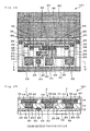
- Fig. 2 is a view illustrating a structure of the pixel 101.
- Fig. 2(a) shows a plan view of the pixel 101
- Fig. 2(b) shows a cross-sectional view taken along a line A-A' in Fig. 2(a).
- some elements are omitted for the purpose of convenience of explanation.
- the pixel 101 is formed on a substrate 10 made of insulating material such as glass, by sequentially stacking a first wiring layer 12, a second wiring layer 14, and a light emitting element layer 16 from the lowest layer side.
- a part of the second wiring layer 14 and the light emitting element layer 16 are also omitted for the purpose of explaining a structure of the first and second wiring layers.
- the first wiring layer 12 comprises signal lines (lines) 20 formed on the substrate 10 and plugs 22 for electrically connecting the signal lines 20 and signal lines (to be described later) included in the second wiring layer. Further, insulating members (for example, silicon oxides, etc.) are formed between the respective signal lines 20 or the respective plugs 22. Further, the insulating members are omitted in Fig. 2(a).
- the second wiring layer 14 comprises signal lines (lines) 30 formed on the first wiring layer 12, plugs 32 for electrically connecting the signal lines 30 and electrodes (to be described later) included in the light emitting element layer 16, a chip 34 for driving the light emitting element layer 16, and a pad group 38 comprising a plurality of pads 36 for electrically connecting the chip 34 to the signal lines 30.
- insulating members for example, silicon oxides, etc.
- the chip 34 is formed on the aforementioned pad group 38.
- the aforementioned chip 34 comprises a plurality of thin film transistors, and controls independently the respective color pixels 1, 2, 3 included in one pixel 101.
- the chip 34 is formed by forming the chips 34 on a substrate (a transfer origin substrate) other than the substrate 10 and peeling off the chips from the transfer origin substrate to transfer them onto the substrate 10. Details of the transfer method will be described later.
- the light emitting element layer 16 comprises three pixel electrodes 40 formed on the second wiring layer 14, a common electrode 42 formed to be opposite to the pixel electrodes 40, three light emitting layers 44 formed between the respective pixel electrodes 40 and the common electrode 42, and a protective layer 46 formed on the common electrode 42. Further, insulating members (for example, silicon oxides, etc.) are formed between the respective pixel electrodes 40 or the respective light emitting layers 44.
- the respective pixel electrodes 40, the respective light emitting layers 44 stacked thereon and the common electrode 42 constitute the three-color pixels 1, 2, 3. Since currents are independently supplied to the respective light emitting layers 44 through the respective pixel electrodes 40 by the aforementioned chip 34, the respective color pixels 1, 2, 3 are independently switched.
- the chip 34 corresponds to the "basic-pixel driving chip” and the "transferred chip".
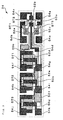
- Fig. 3 is a plan view illustrating an internal structure of the chip 34.
- TFTs thin film transistors
- Fig. 3 in order to facilitate the understandings of structures of thin film transistors (TFTs) or lines included in the chip 34, elements provided on a top surface of the thin film transistors are omitted. The elements, which are omitted, will be described later.
- the chip 34 comprises three switching thin film transistors ST1, ST2, ST3 arranged vertically at the right side, and three driving thin film transistors DT1, DT2, DT3 arranged horizontally at the left side.
- a pixel circuit constructed by combining one switching thin film transistor and one driving thin film transistor drives one color pixel.
- the switching thin film transistor ST1 shown in Fig. 3 operates the driving thin film transistor DT1 in accordance with an input signal (a scanning signal).
- the driving thin film transistor DT1 controls a current flowing in the light emitting layer 44 constituting the color pixel 1.
- the pixel circuit constructed by combining the switching thin film transistor ST2 and the driving thin film transistor DT2 controls a current flowing in the light emitting layer 44 constituting the color pixel 2.
- the pixel circuit constructed by combining the switching thin film transistor ST3 and the driving thin film transistor DT3 controls a current flowing in the light emitting layer 44 constituting the color pixel 3.
- the respective switching thin film transistors and the respective driving thin film transistors described above comprise a first wiring layer and a semiconductor film for forming an active region of a thin film transistor. Furthermore, the respective switching thin film transistors and the respective driving thin film transistors described above further comprise a semiconductor layer formed on the first wiring layer and a second wiring layer formed on the semiconductor layer.
- the first wiring layer is indicated by a white color against a black background
- the semiconductor layer is indicated by a coarse hatching inclined downwardly
- the second wiring layer is indicated by a fine hatching inclined upwardly.
- insulating layers made of SiO 2 are formed between the respective layers.
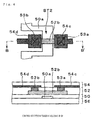
- Fig. 4 is a partial cross-sectional view illustrating a layer structure of the chip 34.
- a plan view of a switching thin film transistor ST2 as an example is shown in Fig. 4(a)
- a cross-sectional view taken along a line B-B' of Fig. 4(a) is shown in Fig. 4(b).
- the chip 34 is constructed by sequentially stacking a first wiring layer 50, a semiconductor layer 52, and a second wiring layer 54 on a base substrate 56.
- the first wiring layer 50 comprises a line 50a serving as a gate electrode of the switching thin film transistor ST2.
- the semiconductor layer 52 comprises a semiconductor film 52b serving as an active region of the switching thin film transistor ST2, and plugs 53a, 53b for electrically connecting the semiconductor film 52b to the second wiring layer 54.
- the second wiring layer 54 comprises lines 54c, 54d serving for supplying current to source/drain regions of the switching thin film transistor ST2.
- other thin film transistors which are not shown, have also the same layer structure as the switching thin film transistor ST2 shown in Fig. 4.
- the first wiring layer 50 comprises lines 50a to 50d.
- the line 50a serves as a gate electrode of the respective switching thin film transistors ST1, ST2, ST3, and also are electrically connected to a line 54a included in the second wiring layer.
- a scanning signal By supplying a scanning signal to the line 50a through the line 54a, operations of the respective switching thin film transistors ST1, ST2, ST3 can be controlled.
- the line 54a is electrically connected to a pad (a connection terminal serving for an electrical connection) provided above the second wiring layer, and the scanning signal is transmitted from outside of the chip 34 to the line 54a through the pad. Details of this pad will be described later.
- the lines for supplying scanning signals to the respective switching thin film transistors ST1, ST2, ST3 as one common line, the area required for formation of the first wiring layer can be decreased and also the number of pads can be reduced, so that the size of the chip 34 can be reduced. Furthermore, by reducing the number of pads (in other words, connecting positions), the frequency at which connection failure occurs in transferring can be reduced. From this point of view, it is also possible to improve the production yield or to reduce the manufacturing cost.
- the line 50b is electrically connected to the semiconductor film 52a, has a function of transmitting the current supplied from the switching thin film transistor ST1 to the driving thin film transistor DT1, and also serves as a gate electrode of the driving thin film transistor DT1.
- the line 50c is electrically connected to the semiconductor film 52b through line 54d included in the second wiring layer, has a function of transmitting the current supplied from the switching thin film transistor ST2 to the driving thin film transistor DT2, and also serves as a gate electrode of the driving thin film transistor DT2.
- the line 50d is electrically connected to the semiconductor film 52c, has a function of transmitting the current supplied from the switching thin film transistor ST3 to the driving thin film transistor DT3, and also serves as a gate electrode of the driving thin film transistor DT3.
- the semiconductor layer 52 comprises semiconductor films 52a to 52f.
- the semiconductor film 52a one end of which is connected to the line 54b and the other end of which is connected to the line 50b, serves as an active region of the switching thin film transistor ST1.
- the semiconductor film 52b one end of which is connected to the line 54c and the other end of which is connected to the line 54d, serves as an active region of the switching thin film transistor ST2.
- the semiconductor film 52c one end of which is connected to the line 54e and the other end of which is connected to the line 50d, serves as an active region of the switching thin film transistor ST3.
- the semiconductor film 52d is connected to the respective lines 54g, 54f, is also connected to a pad (not shown herein) to be described later, and serves as an active region of the driving thin film transistor DT1.
- the semiconductor film 52e is connected to the respective lines 54h, 54i, is also connected to a pad (not shown herein) to be described later, and serves as an active region of the driving thin film transistor DT2.
- the semiconductor film 52f is connected to the respective lines 54j, 54k, is also connected to a pad (not shown herein) to be described later, and serves as an active region of the driving thin film transistor DT3.
- the second wiring layer 54 comprises lines 54a to 54k.
- pads formed above the second wiring layer 54 and serving for electrically connecting the internal circuit of the chip 34 to an external device will be described, including the connection relations to the lines 54a to 54k.
- Fig. 5 is a view illustrating the pads. As shown in Fig. 5, ten pads 56a to 56j are provided above the second wiring layer 54 of the chip 34. In this embodiment, each pad 56a, etc. is formed as a projection portion having a rectangular shape. These pads 56a to 56j are constructed to correspond to the respective pads 36 (see Fig. 2) included in the aforementioned pixel 101 one to one.
- the chip 34 is bonded in a state in which the chip 34 shown in Fig. 5 is inversed and thus the respective pads 56a to 56j are opposite to the respective pads 36 of the pad group 38 included in the pixel 101 shown in Fig. 2 described above. The bonding method of the chip 34 will be described later.
- the pad 56a is electrically connected to the line 54a through the plug 55a.
- the switching transistors ST1 to ST3 are driven.
- the pad 56b is electrically connected to the line 54b through the plug 55b.
- the active region of the switching thin film transistor ST1 is supplied with the current.
- the pad 56c is electrically connected to the line 54c through the plug 55c.
- the active region of the switching thin film transistor ST2 is supplied with the current.
- the pad 56d is electrically connected to the line 54e through the plug 55d.
- the active region of the switching thin film transistor ST3 is supplied with the current.
- the pad 56e is electrically connected to the line 54f through the plug 55e.
- the active region of the driving thin film transistor DT1 is supplied with the current.
- the pad 56f is electrically connected to the line 54g through the plug 55f.
- the pad 56f is electrically connected to one of the aforementioned pads 36. Furthermore, the current output from the driving thin film transistor DT1 is supplied to the color pixel 1 through the line 54g, the plug 55f, the pad 56f and the pad 36 electrically connected to the pad 56f.
- the pad 56g is electrically connected to the line 54h through the plug 55g.
- the active region of the driving thin film transistor DT2 is supplied with the current.
- the pad 56h is electrically connected to the line 54i through the plug 55h.
- the pad 56h is electrically connected to one of the aforementioned pads 36.
- the current output from the driving thin film transistor DT2 is supplied to the color pixel 2 through the line 54i, the plug 55h, the pad 56h and the pad 36 electrically connected to the pad 56h.
- the pad 56i is electrically connected to the line 54j through the plug 55i.
- the active region of the driving thin film transistor DT3 is supplied with the current.
- the pad 56j is electrically connected to the line 54k through the plug 55j.
- the pad 56j is electrically connected to one of the aforementioned pads 36. Furthermore, the current output from the driving thin film transistor DT3 is supplied to the color pixel 3 through the line 54k, the plug 55i, the pad 56i and the pad 36 electrically connected to the pad 56i.
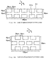
- Fig. 6 is a view illustrating the arrangement of the respective pads provided on the chip 34.
- Fig. 6(a) is a view illustrating an arrangement of pads according to this embodiment.
- Fig. 6(b) is a view illustrating an arrangement of pads according to a comparison example.
- the respective pads 56a to 56j are arranged such that five pads are arranged in a longitudinal direction (shown as an X direction) of the chip 34 and two pads are arranged in an Y direction perpendicular to the longitudinal direction (5 ⁇ 2 array).
- the respective pads are arranged apart from one another by a predetermined distance (10 ⁇ m in the shown example) properly established in consideration of various conditions in design or manufacture.
- the number of pads 56a to 56j is 10, a size of each pad is 24 ⁇ m ⁇ 15 ⁇ m, and a gap between the respective pads is 10 ⁇ m. Further, these numerals are determined in consideration of performance of the manufacturing process, designs or the like, but do not restrict the present invention.
- the chip 34 according to this embodiment has the aforementioned configuration, and a method of manufacturing an organic EL display device according to this embodiment will be next described.
- a transfer technique in which a plurality of chips 34 described above is formed on a transfer origin substrate, and thereafter the chips 34 are peeled off from the first substrate to transfer the chips onto a substrate constituting the organic EL display device, is employed.
- a method of transferring the chips 34 will be mainly described in detail.
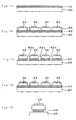
- Figs. 7 and 8 are views illustrating the manufacture method according to this embodiment.
- the transfer method comprises first to fifth steps to be described as follows.
- a peeling layer (light-absorbing layer) 62 is formed on a transfer origin substrate 60.
- the transfer origin substrate 60 have a light transmitting property such that a light can pass through it. By doing so, a light can be irradiated to the peeling layer through the transfer origin substrate to separate the peeling layer rapidly and accurately by the light irradiation.
- the light transmittance be 10% or more and it is more preferable that the light transmittance be 50% or more. This is because light loss is decreased with increase of the transmittance and thus less quantity of light is required for separating the peeling layer 62.
- the transfer origin substrate 60 be made of material having a high reliability, and it is more preferable that it be made of material excellent in heat resistance.
- the process temperature may be increased (for example, about 350 to 1000°C) depending upon their kinds or methods of forming the same.
- the excellent heat resistance of the transfer origin substrate 60 can also increase a range of film forming conditions such as temperature or the like in forming the chips 34 on the transfer origin substrate 60. By doing so, it is possible to perform a desired high-temperature process when a plurality of chips is formed on the transfer origin substrate, so that elements or circuits having high reliability and high performance can be manufactured.
- the transfer origin substrate 60 be made of material having a strain point of Tmax or more.
- the material constituting the transfer origin substrate 60 has preferably a strain point of 350°C or more, and more preferably 500°C or more.
- This material includes heat resistant glass such as quartz glass, Corning 7059, and NEC Glass OA-2.
- the thickness of the transfer origin substrate 60 is not particularly limited, it should preferably be about 0.1 to 5.0 mm, and more preferably about 0.5 to 1.5 mm. This is because light loss is'less likely to occur in cases where a thicker transfer origin substrate 60 has a greater strength and a thinner transfer origin substrate 60 has a lower transmittance.
- the transfer origin substrate 60 with a higher light transmittance may be thicker than the aforementioned maximum range. Furthermore, it is preferable that the transfer origin substrate 60 have a uniform thickness in order to allow uniform light radiation.
- the transfer origin substrate as described above involves a number of conditions, but because the transfer origin substrate can be used repeatedly unlike transfer destination substrates to be final products, even if the material is relatively expensive, it is possible to minimize increase in manufacturing cost by reusing the material.
- a material that results in separation within the layer and/or at the interface (hereinafter, referred to as "intra-layer separation” and/or “interfacial separation”) when absorbing irradiated light should be selected for the peeling layer 62. It is preferable that the light irradiation should eliminate or diminish the bonding force between the atoms or molecules in the material forming the peeling layer 11, that is, result in ablation to cause the intra-layer separation and/or the interfacial separation.
- the light irradiation may result in the release of gas from the peeling layer 62, leading to separation. That is, a component contained in the peeling layer 62 may be gasified and then released, and the peeling layer 62 may be temporarily gasified by absorbing the light, so that the vapor thereof is released to contribute to separation.
- a composition of the peeling layer 62 includes, for example, the following A to F.
- the peeling layer can be made of an alloy containing nitrogen. That is because exposing a peeling layer made of an alloy containing nitrogen to light will result in the release of the nitrogen, thereby promoting the separation of the peeling layer.
- the peeling layer may comprise a multilayer film.
- a multilayer film can be formed, for example, by stacking an amorphous silicon film and a metal film formed thereon.
- Materials for the multilayer film can include at least one material from among the aforementioned ceramics, metals, and organic polymer materials.
- a method of forming the peeling layer 62 is not particularly limited, but may be selected in accordance with various conditions such as the film composition and the film thickness.
- Examples of the method of forming the peeling layer include various vapor phase film-forming methods such as CVD and sputtering, various types of plating methods, coating methods such as spin coating or the like, various types of printing methods, transfer methods, ink jet coating methods and powder jet methods, and combinations of two or more of the above.
- an intermediate layer may be provided between the transfer origin substrate 60 and the peeling layer 62 for the purpose of improvement of close adherence between both, in accordance with features of the transfer origin substrate 60 and the peeling layer 62.
- the intermediate layer has at least one of, for example, functions as a protective layer for physically or chemically protecting the transferred layer at the time of manufacture or use, an insulating layer, a barrier layer for preventing components from being diffused (migration) to or from the transferred layer and a reflective layer.
- a second process will be described.
- a plurality of chips 34 is formed on the peeling layer 62.
- a layer comprising the plurality of chips 34 is referred to as a transferred layer 64.
- the respective chips 34 comprise six thin film transistors as described above.
- the manufacturing method of this embodiment after manufacturing the thin film transistors on the transfer origin substrate satisfying various manufacture conditions, it is possible to transfer the thin film transistors onto a final substrate not satisfying the manufacture conditions. That is, according to the manufacturing method of this embodiment, since a substrate made of cheaper materials can be used as the final substrate, it is possible to reduce the manufacturing cost, and since a flexible substrate having flexibility can be used, it is possible to broaden a range of selecting the final substrate.
- separation of the respective chips 34 in the transferred layer 64 will be described.
- a method of separating the respective chips 34 a method of separating the respective chips by etching, a method of not providing a particular structure for separation, a method of separating only a peeling layer, a method of facilitating the separation into the individual transferred bodies by forming a predetermined structure on the transfer origin substrate and so on can be considered.
- the method of completely separating the individual chips 34 will be described.
- grooves 62c having a trenched structure are formed in circumferential edges of regions corresponding to the chips 34 by a wet etching or a dry etching to leave the respective chips 34 in island shapes.
- These grooves 62c cut out the overall transferred layer 64 and the overall (see Fig. 7(c)) or partial (see Fig. 7(d)) peeling layer 62 in the thickness direction of the substrate. The cutting may be performed only to the transferred layer 64 more shallowly.
- Theses grooves 62c may be formed not only by etching a part of the peeling layer 62 as shown in Fig. 7(d), but also by completely etching the peeling layer 62 as shown in Fig.
- the peeling layer may be over-etched such that the adhesive area of the peeling layer 62 to the chip 34 becomes smaller than the overall area of an adhesive surface of the transferred body to the peeling layer. Since the area of the peeling layer 62 becomes smaller by over-etching the peeling layer, the separation can be surely executed with only a small force by the light irradiation to the peeling layer 62, and by decreasing the area of the peeling layer 62, the quantity of light energy required for separation can be decreased.
- the peeling layer 62 may be left to be continuous. Only if sufficient energy can be applied to regions in which the chips 34 are formed, the peeling layer 62 in the regions can be surely separated. For this reason, even if the grooves are not formed in the peeling layer 62, it is possible to peel off only the desired transferred bodies.
- the aforementioned substrate 10 (see Fig. 2) on which the first wiring layer 12 is formed and the signal lines 30 and the pads 36 are formed on the first wiring layer 12 corresponds to the transfer destination substrate 66 as shown Fig. 8(a). Further, the respective pads 36 included in the transfer destination substrate 66 are brought into contact with the respective pads 56a to 56j provided on the chips 34 to be targets for transfer, and then the attachment of the chips 34 is performed.
- Suitable examples of the adhesive constituting the aforementioned adhesive layer 68 can include various types of curing adhesives such as reaction-curing adhesive, thermosetting adhesive, light-curing adhesive such as ultraviolet-curing adhesive, anaerobe-curing adhesive.
- the adhesives may include, for example, any of epoxy adhesives, acrylate adhesives, silicon adhesives and so on.
- the adhesives to be used may be adjusted to have a viscosity suitable for application thereof by adding proper solvent to the adhesives.
- the adhesive layer 68 is formed only on the chips 34 to be transferred or only in regions on the transfer destination substrate 66 corresponding to the chips 34 to be transferred.
- This local formation of the adhesive layer 68 can be performed by employing various printing methods or liquid ejection methods.
- the liquid ejection methods include a piezo-jet method of ejecting liquid using deformation of piezoelectric bodies and a method of ejecting liquid by generating bubbles from heating.
- the adhesive layer 68 is formed, for example, using an inkjet coating (liquid ejection) method.
- the separation (the intra-layer separation and/or the interfacial separation) can occur only in the peeling layer 62 supporting the chips 34 to be transferred.
- the intra-layer separation and/or the interfacial separation of the peeling layer 62 results from generation of ablation in the material constituting the peeling layer 62, and phase transformations such as release of gas contained in the peeling layer 62, dissolution or transpiration occurring right after the light irradiation.
- the "ablation” means that the fixing material (a material constituting the peeling layer 62) having absorbed the irradiated light is excited photo-chemically or thermally and thus the bonding between atoms or molecules of the surface or inner part thereof is disconnected to release the atoms or molecules, and mainly means that all or a part of materials constituting the peeling layer 62 causes the phase transformation such as dissolution or transpiration (gasification). Further, a fine-bubbled state can result from the phase transformation to reduce the adhesive force.
- the peeling layer 62 undergoes the intra-layer separation, the interfacial separation, or both is governed by the composition of the peeling layer 62 and various other factors, examples of which include conditions such as the type of light that is irradiated, its wavelength, its intensity, and the depth to which it reaches.
- the light L that is irradiated may be any that brings about the intra-layer separation and/or the interfacial separation in the peeling layer 62, such as X-ray, UV-ray, visible light, IR-ray, laser light.
- the laser light is preferred because it readily produces separation (ablation) in the peeling layer 62 and is capable of high-precision irradiation of certain areas.
- the laser light with a wavelength of 100 nm to 350 nm is preferred.
- the use of such short wavelength laser light can provide higher irradiation precision and more effective separation in the peeling layer 62.
- excimer laser is used very suitably. Since the excimer laser outputs a high energy laser light in the short wavelength region, the ablation can be generated in the peeling layer 62 for a very short time, and thus it is possible to separate the peeling layer 62 without almost causing increase in temperature of the transfer destination substrate 66 or the first substrate 60 which is adjacent and without causing damage such as deterioration in the chips 34.
- the wavelength of the laser light to be irradiated be about 350 nm to 1200 nm. Since laser light sources or illumination devices which are widely used in the field of general processing, such as YAG and gas lasers, can be used for laser light with such a wavelength, the light irradiation can be performed inexpensively and simply. Further, by using such laser light with a wavelength in the visible light region, a degree of freedom in selecting the transfer origin substrate 60 can be increased, as long as the transfer origin substrate 60 is permeable to visible light.
- the energy density of the laser light to be irradiated should be preferably about 10 to 5000 mJ/cm 2 , and more preferably about 100 to 500 mJ/cm 2 .
- the irradiation time should be preferably about 1 to 1000 nsec, and more preferably about 10 to 100 nsec. A higher energy density or longer irradiation time will more readily result in ablation, whereas a lower energy density or shorter irradiation time can minimize the risk of adverse effects on chips 34 or the like by the irradiated light passing through the peeling layer 62.
- the transfer origin substrate 60 is separated from the transfer destination substrate 66. Since the peeling layer 62 of the chips 34 to be transferred to the transfer destination substrate 66 is peeled off from the chips 34, the chips 34 to be transferred are cut off from the transfer origin substrate 60 side, through the fourth process. Furthermore, the chips 34 to be transferred are attached to the transfer destination substrate 66 through the adhesive layer 68.
- the peeling layer 62 be peeled off completely, but the peeling layer 62 may be peeled off partially only if the bonding intensity of the chips 34 to be transferred to the adhesive layer 68 is larger than the bonding force by the remaining peeling layer 62 and as a result, when the transfer origin substrate 60 is separated from the transfer destination substrate 66, the chips 34 to be transferred can be surely transferred to the transfer destination substrate 66.
- whether the transferred bodies can be transferred or not is determined by a relative force relation between the bonding force of the peeling layer weakened due to separation of the peeling layer and the bonding force of the adhesive layer applied to the transferred bodies. If the separation by the peeling layer is sufficient, it is possible to transfer the transferred bodies even when the bonding force of the adhesive layer is weak, but even if the separation by the peeling layer is not sufficient, it is possible to transfer the transferred bodies even when the bonding force of the adhesive layer is intensive.
- the chips 34 are transferred to desired positions on the transfer destination substrate 66. Thereafter, by forming an insulating member covering the chips 34 or the like, the second wiring layer 14 which is shown in Fig. 2 is formed, and by forming the light emitting element layers 16 on the second wiring layer 14, the organic EL display device 100 is formed.
- a proper method for removing the residuals of the peeling layer 62 can be selected and employed from methods such as cleaning, etching, ashing, polishing or combinations thereof.
- the transfer origin substrate 60 can be provided for reuse (recycle) thereof. By reusing the transfer origin substrate 60, waste of the manufacturing cost can be prevented. This is specifically effective for using the transfer origin substrate 60 made of expensive material or rare material such as quartz glass.
- the chips 34 combining the functions of driving the three-color pixels 1, 2, 3 included in one pixel 101, respectively, are formed on the transfer origin substrate 60 and then the transfer thereof is performed, the number of transfers is 1 every pixel 101. For this reason, since the number of transferred bodies can be reduced and thus the number of transfers can be reduced, the number of occurrences of transfer error can be reduced as much and thus it is possible to enhance the production yield.
- FIG. 9 is a view illustrating specific examples of electronic apparatuses to which the organic EL display device 100 according to this embodiment applies.
- Fig. 9(a) is an example of application to a portable phone, wherein a portable phone 230 comprises an antenna unit 231, a voice output unit 232, a voice input unit 233, a manipulation unit 234, and the organic EL display device 100 according to this embodiment.
- the display device according to the present invention is usable as a display unit.
- Fig. 9(b) is an example of application to a video camera, wherein a video camera 240 comprises an image reception unit 241, a manipulation unit 242, a voice input unit 243, and the organic EL display device 100 according to this embodiment.
- the display device according to the present invention is usable as a finder or a display unit.
- Fig. 9(c) is an example of application to a portable personal computer, wherein a computer 250 comprises a camera unit 251, a manipulation unit 252 and the organic EL display device 100 according to this embodiment.
- the display device according to the present invention is usable as a display unit.
- Fig. 9(d) is an example of application to a head mount display, wherein a head mount display 260 comprises a band 261, an optical system reception unit 262, and the organic EL display device 100 according to this embodiment.
- the display device according to the present invention is usable as an image display source.
- the display device 100 is not limited to the aforementioned examples, but may apply to a variety of electronic apparatuses such as a facsimile device having a display function, a finder of a digital camera, a portable TV, electronic organizers or the like.
- the present invention is not limited to the aforementioned embodiment, but a variety of modifications can be made within the scope of the present invention.
- the organic EL display device is described as an example of the electro-optical device according to the present invention, the present invention is not limited to this, but may apply to electro-optical devices employing various electro-optical elements (for example, plasma emission elements, electrophoresis elements, liquid crystal elements or the like).
Landscapes
- Physics & Mathematics (AREA)
- Nonlinear Science (AREA)
- Mathematical Physics (AREA)
- Engineering & Computer Science (AREA)
- Chemical & Material Sciences (AREA)
- Crystallography & Structural Chemistry (AREA)
- Microelectronics & Electronic Packaging (AREA)
- General Physics & Mathematics (AREA)
- Optics & Photonics (AREA)
- Electroluminescent Light Sources (AREA)
- Devices For Indicating Variable Information By Combining Individual Elements (AREA)
- Thin Film Transistor (AREA)
- Liquid Crystal (AREA)
- Electrochromic Elements, Electrophoresis, Or Variable Reflection Or Absorption Elements (AREA)
Abstract

Description
- The present invention relates to a display device (an electro-optical device) in which pixels are driven using elements such as thin film transistors or the like, and a method of manufacturing the same.
- In display devices (electro-optical devices) using thin film transistors for driving pixels, such as liquid crystal display devices to be driven with thin film transistors, organic electroluminescent (EL) display devices to be driven with thin film transistors, light-emitting diode display devices to be driven with thin film transistors, electrophoresis display devices to be driven with thin film transistors or the like, the thin film transistors constitute only a part of the overall device, and lines, support substrates, etc. constitute the rest of the overall device. When these display devices (the display devices to be driven with thin film transistors) are manufactured by forming thin film transistors, the lines, and the support substrate into a single body through the same manufacturing process, since a difficult and complex manufacturing process is required for manufacturing the thin film transistors, the manufacturing cost thereof is generally high. However, since the difficult and complex manufacturing process is not required only for the lines and the support substrate, the manufacturing cost thereof is low. Therefore, if the thin film transistors and the lines or support substrate can be manufactured separately and the thin film transistors can be arranged only in desired positions, the manufacturing cost of the display devices to be driven with thin film transistors can be reduced.
- For such requirement, a transfer method of forming elements in desired positions on a transfer destination base substrate has been developed, by forming a transferred layer comprising elements such as thin film transistors inserting a peeling layer between the transferred and the transfer origin base substrate, attaching it to a transfer destination base substrate, irradiating light into the peeling layer to peel off the peeling layer and to separate the transfer origin base substrate from the peeling layer. Such transfer method is disclosed, for example, in Japanese Unexamined Patent Application Publication No. 10-125931 (Patent Document 1). Since the thin film transistors can be formed only in desired positions using the aforementioned transfer method, the manufacturing cost of the display device to be driven with thin film transistors can be reduced as a whole. Further, at that time, the peeling-off or transferring process employs laser ablation or adhesive (T. Shimoda, et al, Techn. Dig. IEDM 1999, 289 (Non-patent Document 1), S. Utsunomiya, et al, Dig. Tech. Pap. SID 2000, 916 (Non-patent Document 2), T. Shimoda, Proc. Asia Display/IDW'01, 327 (Non-patent Document 3), S. Utsunomiya, et al, Proc. Asia Display/IDW'01, 339 (Non-patent Document 4), S. Utsunomiya, et al, AM-LCD'02, to be presented (Non-patent Document 5)).
- [Patent Document 1]
Japanese Unexamined Patent Application Publication No. 10-125931 - [Non-patent Document 1]
T. Shimoda, et al, Techn. Dig. IEDM 1999, 289 - [Non-patent Document 2]
S. Utsunomiya, et al, Dig. Tech. Pap. SID 2000, 916 - [Non-patent Document 3]
T. Shimoda, Proc. Asia Display/IDW'01, 327 - [Non-patent Document 4]
S. Utsunomiya, et al, Proc. Asia Display/IDW'01, 339 - [Non-patent Document 5]
S. Utsunomiya, et al, AM-LCD'02, to be presented - When the display device is manufactured using the aforementioned transfer method, production yield is inclined to be decreased with increase in the number of transferred bodies which are targets to be transferred from a transfer origin base substrate to a transfer destination base substrate.
- Although electrical connections between elements included in the transferred bodies and lines included in the transfer destination base substrate may be often made by previously forming pads (connection terminals serving as the electrical connections) on the transferred bodies and the transfer destination base substrate correspondingly to each other, in this case, the production yield is inclined to be decreased with increase in the number of pads.
- Furthermore, since the number of transferred bodies capable of being formed on the transfer origin base substrate can be increased and decreased with largeness and smallness of an area of each transferred body, the manufacturing cost may depend upon the area.
- Therefore, it is an object of the present invention to enhance the production yield of a display device.
- Further, it is another object of the present invention to reduce the manufacturing cost of a display device.
- In order to accomplish the above objects, the present invention provides a method of manufacturing an electro-optical device including a display region in which a plurality of basic pixels is arranged, each basic pixel comprising a plurality of color pixels, the method comprising: a substrate line forming step of forming the lines on a first substrate for driving a plurality of electro-optical elements respectively constituting the color pixels, correspondingly to the arrangement of the basic pixels; a basic-pixel driving-chip forming step of forming on a second substrate, as a chip to be transferred to each basic pixel, a drive circuit for driving the plurality of electro-optical elements which constitutes the plurality of color pixels of each basic pixel to obtain a plurality of basic-pixel driving chips; and a basic-pixel driving-chip transferring step of transferring the respective basic-pixel driving chips from the second substrate onto the first substrate, and connecting the drive circuits to regions of the lines corresponding to the basic pixels.
- Here, the "electro-optical elements" in the present invention include elements such as electroluminescent (EL) elements, electrical emission elements, plasma emission elements, electrophoresis elements, liquid crystal elements, LEDs or the like. Further, in the present invention, "as a chip transferable" means that the respective basic-pixel driving chips (transferred bodies) are formed on a second substrate to allow the respective basic-pixel driving chips to be physically dividable in order to be individually targets for transfer, but is not necessarily limited to separation (or division) into a single chip.
- For example, when one basic pixel comprises three-color pixels, it can be considered that the elements (transferred bodies) such as thin film transistors are transferred correspondingly to each of the three-color pixels. In this case, the number of transfers for the respective basic pixels is 3.
- On the contrary, in the present invention, since the basic-pixel driving chips, in which functions of driving the plurality of color pixels included in one basic pixel are incorporated into one chip, are formed on the second substrate and then the peeling and transferring is performed, the number of transfers for the respective basic pixels is 1. That is, in the present invention, since the number of transferred bodies can be decreased and the number of transfers can be reduced, it is easy to avoid disadvantages such as transfer failure as much, so that it is possible to enhance the production yield.
- Preferably, each of the basic-pixel driving chips comprises a plurality of control means for individually controlling operating conditions of the plurality of electro-optical elements.
- The respective control means can be implemented by constructing circuit active elements such as thin film transistors which are formed as a single body, or the active elements of which are formed plurally, or the active elements of which are properly combined with passive elements such as capacitors. By providing the control means to correspond to the respective electro-optical elements one to one, the configuration of the drive circuit included in the basic-pixel driving chip can be simplified, thereby facilitating the design or manufacture.
- Preferably, each of the control means comprises a first transistor for controlling current flowing in the electro-optical element and a second transistor for operating the first transistor in accordance with input signals.
- Like above, by constructing different transistors serving for a function of supplying a driving current to an electro-optical element and a function of controlling a selection/non-selection condition of the electro-optical element, respectively, it is possible to implement a basic-pixel driving chip very suitable for driving electro-optical elements (for example, EL elements, etc.) requiring relative large driving current.
- Preferably, a gate electrode of the second transistor included in each of the control means is connected to a common line passing through each of the control means.
- By doing so, since the number of lines can be reduced compared with a case in which lines are provided individually in the gate electrodes of the second transistors, it is possible to reduce a chip size of the basic-pixel driving chip. As a result, since more basic-pixel driving chips, which are transferred bodies, can be formed on the transfer origin substrate (second substrate), it is possible to reduce the manufacturing cost. Furthermore, reduction of the number of lines allows the degree of freedom in designing the layout of lines in chips to be increased.
- Furthermore, since the connection positions for electrically connecting external devices to the drive circuit provided in the basic-pixel driving chip become small, it is possible to decrease the chip size. Furthermore, decrease in the connection positions allows the frequency of connection failure in transfer to be decreased. For these reasons, it is possible to enhance of the production yield or to reduce the manufacturing cost.
- Preferably, each of the basic-pixel driving chips comprises a plurality of first connection terminals serving as electrical connection to the basic-pixel driving chip; the first substrate comprises a plurality of second connection terminals provided in regions to which the basic-pixel driving chips are transferred in one-to-one correspondence with the first connection terminals and serving for electrical connection to the lines; in the basic-pixel driving-chip transferring step, the electrical connection between the basic-pixel driving chips and the first substrate is accomplished by carrying out the transferring to bring the plurality of first and second connection terminals into contact with each other; and each of the first connection terminals and each of the second connection terminals are allocated to the common line included in the basic-pixel driving chip and to the lines on the first substrate to be electrically connected to the common line, respectively.
- By doing so, since the number of connection terminals (pads) serving for electrical connection can be reduced, it is possible to enhance the production yield due to decrease in the connection positions. Furthermore, the chip size of the basic-pixel driving chip can be decreased and thus it is possible to reduce the manufacturing cost.
- Preferably, the basic-pixel driving-chip transferring step comprises a step of forming an adhesive layer on at least one side of the first connection terminals formed in the basic-pixel driving chips or the second connection terminals formed on the first substrate. By doing so, it is possible to more firmly connect the first and second connection terminals.
- Preferably, the plurality of first connection terminals is spaced from one another by a predetermined distance, and also is arranged in two lines along one direction of the basic-pixel driving chip. By doing so, since the area required for arrangement of the plurality of first connection terminals can be decreased, it is possible to reduce the chip size of the basic-pixel driving chip. Furthermore, by arranging the first connection terminals as described above, it is possible to decrease the area required for arrangement of the second connection terminals which should be arranged in one-to-one correspondence with the first connection terminals.
- Preferably, the basic-pixel driving-chip forming step comprises a step of forming a peeling layer interposed between the second substrate and the basic-pixel driving chips, the peeling layer having a feature that application of energy causes a phase transformation to weaken the bonding strength to the basic-pixel driving chips. By doing so, it is easy to peel off the basic-pixel driving chips from the second substrate in transfer. Furthermore, it can be considered that various methods such as a method of applying heat or a method of irradiating light are used as a method of applying energy, and the method of irradiating light using laser light is specifically preferable. According to the light irradiation method, energy can be applied to any region and in addition accurate positioning is possible.
- Furthermore, the present invention provides a transferred chip to be used for manufacturing an electro-optical device in which a plurality of basic-pixel circuits is arranged on a wiring substrate, the transferred chip comprising: drive circuits for driving the basic-pixel circuits; and a plurality of connection terminals for connecting the wiring substrate to the drive circuits, wherein the plurality of connection terminals is formed in patterns of two lines all over a transfer surface of the transferred chip.
- Here, the "transferred chip" means a minimum unit as a transferred body in using the aforementioned transfer technique, specifically, the separation and transfer technique in which a transferred body is first formed on a substrate which is a transfer origin, and then the transferred body is transferred onto a transfer destination substrate (for example, a substrate constituting the final product) other than the transfer origin substrate, and the transferred chip comprises a circuit including various elements or combination of them to serve for a predetermined function.
- By the aforementioned construction according to the present invention, the area required for arrangement of the plurality of connection terminals can be decreased, and as a result, it is possible to reduce the chip size of the transferred chip. For this reason, since more basic-pixel driving chips, which are the transferred bodies, can be formed on the transfer origin substrate (second substrate), it is possible to reduce the manufacturing cost.
- Preferably, the basic-pixel circuits comprise a plurality of electro-optical elements constituting a plurality of color pixels, respectively, and the drive circuits drive and control each of the plurality of electro-optical elements. As a result, configuration of the drive circuit is simplified to facilitate a design or a manufacture thereof, so that it is possible to accomplish reduction of the manufacturing cost.
- Furthermore, the present invention provides a transfer origin substrate constructed by forming a plurality of the aforementioned transferred chips according to the present invention on a substrate. Furthermore, it is preferable that the transfer origin substrate further comprise a peeling layer interposed between the substrate and the transferred chips, the peeling layer having a feature that application of energy thereto causes a phase transformation to weaken the bonding strength to the transferred chips.
- Furthermore, the present invention provides an electro-optical device manufactured using the aforementioned manufacturing method. Further, the present invention provides an electro-optical device manufactured using the aforementioned transferred chip or the aforementioned transfer origin substrate. As a result, it is possible to reduce the cost and the production yield for the electro-optical device. Furthermore, in the present invention, the "electro-optical device" includes display devices comprising various electro-optical elements such as electroluminescent (EL) elements, electrical emission elements, plasma emission elements, electrophoresis elements, liquid crystal elements or the like.
- Furthermore, the present invention provides an electronic apparatus using the aforementioned electro-optical device according to the present invention as a display unit. Here, the electronic apparatus includes a video camera, a portable phone, a personal computer, a portable information terminal device (so-called PDA) or other various types. By using the electro-optical device according to the present invention, since the display unit can be constructed with low cost, it is possible to decrease the cost for the electronic apparatus.
- Embodiments of the present invention will now be described by way of further example only and with reference to the accompanying drawings, in which:-
- Fig. 1 is a view schematically illustrating a configuration of an organic EL display device.
- Fig. 2 is a view illustrating a structure of a pixel.
- Fig. 3 is a plan view illustrating an internal structure of a chip.
- Fig. 4 is a partial cross-sectional view illustrating a layer structure of the chip.
- Fig. 5 is a view illustrating a pad.
- Fig. 6 is a view illustrating arrangement of the respective pads provided on the chip.
- Fig. 7 is a view illustrating a manufacturing method according to this embodiment.
- Fig. 8 is a view illustrating a manufacturing method according to this embodiment.
- Fig. 9 is a view illustrating specific examples of an electronic apparatus to which the organic EL display device can apply.
- Now, a structure and a manufacturing method of a display device to be driven with thin film transistors according to an embodiment of the present invention will be described in detail. In this embodiment, an organic EL display device will be described as an example of the display device to be driven with thin film transistors.
- Fig. 1 is a view schematically illustrating a configuration of the organic EL display device according to this embodiment. In the organic
EL display device 100 shown in Fig. 1, a plurality of pixels (basic pixels) 101, each of which comprises three-color pixels - Among the color pixels, for example, the
color pixel 1 corresponds to a red color, thecolor pixel 2 corresponds to a green color, and thecolor pixel 3 corresponds to a blue color. Therespective pixels 101 are driven by chips having a drive circuit built in, the drive circuit comprising a plurality of thin film transistors (TFTs). - Fig. 2 is a view illustrating a structure of the
pixel 101. Fig. 2(a) shows a plan view of thepixel 101, and Fig. 2(b) shows a cross-sectional view taken along a line A-A' in Fig. 2(a). Further, in Fig. 2(a), some elements are omitted for the purpose of convenience of explanation. - As shown in Fig. 2, the
pixel 101 is formed on asubstrate 10 made of insulating material such as glass, by sequentially stacking afirst wiring layer 12, asecond wiring layer 14, and a light emittingelement layer 16 from the lowest layer side. In Fig. 2(a), a part of thesecond wiring layer 14 and the light emittingelement layer 16 are also omitted for the purpose of explaining a structure of the first and second wiring layers. - The
first wiring layer 12 comprises signal lines (lines) 20 formed on thesubstrate 10 and plugs 22 for electrically connecting thesignal lines 20 and signal lines (to be described later) included in the second wiring layer. Further, insulating members (for example, silicon oxides, etc.) are formed between therespective signal lines 20 or the respective plugs 22. Further, the insulating members are omitted in Fig. 2(a). - The
second wiring layer 14 comprises signal lines (lines) 30 formed on thefirst wiring layer 12, plugs 32 for electrically connecting thesignal lines 30 and electrodes (to be described later) included in the light emittingelement layer 16, achip 34 for driving the light emittingelement layer 16, and apad group 38 comprising a plurality ofpads 36 for electrically connecting thechip 34 to the signal lines 30. Further, although omitted in Fig. 2(a), insulating members (for example, silicon oxides, etc.) are formed between therespective signal lines 30 or the respective plugs 32. Furthermore, although thechip 34 is omitted in Fig. 2(a), thechip 34 is formed on theaforementioned pad group 38. - In this embodiment, the
aforementioned chip 34 comprises a plurality of thin film transistors, and controls independently therespective color pixels pixel 101. Thechip 34 is formed by forming thechips 34 on a substrate (a transfer origin substrate) other than thesubstrate 10 and peeling off the chips from the transfer origin substrate to transfer them onto thesubstrate 10. Details of the transfer method will be described later. - The light emitting
element layer 16 comprises threepixel electrodes 40 formed on thesecond wiring layer 14, acommon electrode 42 formed to be opposite to thepixel electrodes 40, three light emittinglayers 44 formed between therespective pixel electrodes 40 and thecommon electrode 42, and aprotective layer 46 formed on thecommon electrode 42. Further, insulating members (for example, silicon oxides, etc.) are formed between therespective pixel electrodes 40 or the respective light emitting layers 44. Therespective pixel electrodes 40, the respectivelight emitting layers 44 stacked thereon and thecommon electrode 42 constitute the three-color pixels light emitting layers 44 through therespective pixel electrodes 40 by theaforementioned chip 34, therespective color pixels - Like above, since by forming intensively drive circuits for the three-color pixels as one
chip 34, the number of chips to be a target for transfer is reduced into 1/3 compared with a case in which thin film transistors are individually transferred for therespective color pixels chip 34 corresponds to the "basic-pixel driving chip" and the "transferred chip". - Next, a specific example of an internal structure of the
chip 34 of this embodiment will be described in detail. - Fig. 3 is a plan view illustrating an internal structure of the
chip 34. In Fig. 3, in order to facilitate the understandings of structures of thin film transistors (TFTs) or lines included in thechip 34, elements provided on a top surface of the thin film transistors are omitted. The elements, which are omitted, will be described later. - As shown in Fig. 3, the
chip 34 comprises three switching thin film transistors ST1, ST2, ST3 arranged vertically at the right side, and three driving thin film transistors DT1, DT2, DT3 arranged horizontally at the left side. - In this embodiment, a pixel circuit constructed by combining one switching thin film transistor and one driving thin film transistor drives one color pixel. Specifically, the switching thin film transistor ST1 shown in Fig. 3 operates the driving thin film transistor DT1 in accordance with an input signal (a scanning signal). The driving thin film transistor DT1 controls a current flowing in the
light emitting layer 44 constituting thecolor pixel 1. Similarly, the pixel circuit constructed by combining the switching thin film transistor ST2 and the driving thin film transistor DT2 controls a current flowing in thelight emitting layer 44 constituting thecolor pixel 2. Furthermore, the pixel circuit constructed by combining the switching thin film transistor ST3 and the driving thin film transistor DT3 controls a current flowing in thelight emitting layer 44 constituting thecolor pixel 3. - The respective switching thin film transistors and the respective driving thin film transistors described above comprise a first wiring layer and a semiconductor film for forming an active region of a thin film transistor. Furthermore, the respective switching thin film transistors and the respective driving thin film transistors described above further comprise a semiconductor layer formed on the first wiring layer and a second wiring layer formed on the semiconductor layer. In Fig. 3, for the purpose of easily understanding the respective layers, the first wiring layer is indicated by a white color against a black background, the semiconductor layer is indicated by a coarse hatching inclined downwardly, and the second wiring layer is indicated by a fine hatching inclined upwardly. Further, insulating layers made of SiO2 are formed between the respective layers.
- Fig. 4 is a partial cross-sectional view illustrating a layer structure of the
chip 34. In Fig. 4, a plan view of a switching thin film transistor ST2 as an example is shown in Fig. 4(a), and a cross-sectional view taken along a line B-B' of Fig. 4(a) is shown in Fig. 4(b). - As shown in Fig. 4(b), the
chip 34 is constructed by sequentially stacking afirst wiring layer 50, asemiconductor layer 52, and asecond wiring layer 54 on abase substrate 56. Thefirst wiring layer 50 comprises aline 50a serving as a gate electrode of the switching thin film transistor ST2. Thesemiconductor layer 52 comprises asemiconductor film 52b serving as an active region of the switching thin film transistor ST2, and plugs 53a, 53b for electrically connecting thesemiconductor film 52b to thesecond wiring layer 54. Thesecond wiring layer 54 compriseslines - Next, referring to Fig. 3, structures of the first wiring layer, the semiconductor layer, and the second wiring layer will be described further in detail.
- The
first wiring layer 50 compriseslines 50a to 50d. Theline 50a serves as a gate electrode of the respective switching thin film transistors ST1, ST2, ST3, and also are electrically connected to aline 54a included in the second wiring layer. By supplying a scanning signal to theline 50a through theline 54a, operations of the respective switching thin film transistors ST1, ST2, ST3 can be controlled. - Further, although not shown in Fig. 3, the
line 54a is electrically connected to a pad (a connection terminal serving for an electrical connection) provided above the second wiring layer, and the scanning signal is transmitted from outside of thechip 34 to theline 54a through the pad. Details of this pad will be described later. In this embodiment, like above, by forming the lines for supplying scanning signals to the respective switching thin film transistors ST1, ST2, ST3 as one common line, the area required for formation of the first wiring layer can be decreased and also the number of pads can be reduced, so that the size of thechip 34 can be reduced. Furthermore, by reducing the number of pads (in other words, connecting positions), the frequency at which connection failure occurs in transferring can be reduced. From this point of view, it is also possible to improve the production yield or to reduce the manufacturing cost. - The
line 50b is electrically connected to thesemiconductor film 52a, has a function of transmitting the current supplied from the switching thin film transistor ST1 to the driving thin film transistor DT1, and also serves as a gate electrode of the driving thin film transistor DT1. - The
line 50c is electrically connected to thesemiconductor film 52b throughline 54d included in the second wiring layer, has a function of transmitting the current supplied from the switching thin film transistor ST2 to the driving thin film transistor DT2, and also serves as a gate electrode of the driving thin film transistor DT2. - The
line 50d is electrically connected to thesemiconductor film 52c, has a function of transmitting the current supplied from the switching thin film transistor ST3 to the driving thin film transistor DT3, and also serves as a gate electrode of the driving thin film transistor DT3. - The
semiconductor layer 52 comprisessemiconductor films 52a to 52f. Thesemiconductor film 52a, one end of which is connected to theline 54b and the other end of which is connected to theline 50b, serves as an active region of the switching thin film transistor ST1. Thesemiconductor film 52b, one end of which is connected to theline 54c and the other end of which is connected to theline 54d, serves as an active region of the switching thin film transistor ST2. Thesemiconductor film 52c, one end of which is connected to theline 54e and the other end of which is connected to theline 50d, serves as an active region of the switching thin film transistor ST3. - The
semiconductor film 52d is connected to therespective lines 54g, 54f, is also connected to a pad (not shown herein) to be described later, and serves as an active region of the driving thin film transistor DT1. The semiconductor film 52e is connected to therespective lines semiconductor film 52f is connected to therespective lines 54j, 54k, is also connected to a pad (not shown herein) to be described later, and serves as an active region of the driving thin film transistor DT3. - The
second wiring layer 54 compriseslines 54a to 54k. Here, pads formed above thesecond wiring layer 54 and serving for electrically connecting the internal circuit of thechip 34 to an external device will be described, including the connection relations to thelines 54a to 54k. - Fig. 5 is a view illustrating the pads. As shown in Fig. 5, ten pads 56a to 56j are provided above the
second wiring layer 54 of thechip 34. In this embodiment, each pad 56a, etc. is formed as a projection portion having a rectangular shape. These pads 56a to 56j are constructed to correspond to the respective pads 36 (see Fig. 2) included in theaforementioned pixel 101 one to one. Thechip 34 is bonded in a state in which thechip 34 shown in Fig. 5 is inversed and thus the respective pads 56a to 56j are opposite to therespective pads 36 of thepad group 38 included in thepixel 101 shown in Fig. 2 described above. The bonding method of thechip 34 will be described later. - The pad 56a is electrically connected to the
line 54a through the plug 55a. By supplying a scanning signal to theline 54a through the pad 56a from an external device, the switching transistors ST1 to ST3 are driven. - The
pad 56b is electrically connected to theline 54b through theplug 55b. By externally supplying a current to theline 54b through thepad 56b, the active region of the switching thin film transistor ST1 is supplied with the current. - The
pad 56c is electrically connected to theline 54c through the plug 55c. By externally supplying a current to theline 54c through thepad 56c, the active region of the switching thin film transistor ST2 is supplied with the current. - The
pad 56d is electrically connected to theline 54e through theplug 55d. By externally supplying a current to theline 54e through thepad 56d, the active region of the switching thin film transistor ST3 is supplied with the current. - The pad 56e is electrically connected to the line 54f through the
plug 55e. By externally supplying a current to the line 54f through the pad 56e, the active region of the driving thin film transistor DT1 is supplied with the current. - The pad 56f is electrically connected to the
line 54g through the plug 55f. The pad 56f is electrically connected to one of theaforementioned pads 36. Furthermore, the current output from the driving thin film transistor DT1 is supplied to thecolor pixel 1 through theline 54g, the plug 55f, the pad 56f and thepad 36 electrically connected to the pad 56f. - The
pad 56g is electrically connected to theline 54h through theplug 55g. By externally supplying a current to theline 54h through thepad 56g, the active region of the driving thin film transistor DT2 is supplied with the current. - The
pad 56h is electrically connected to theline 54i through theplug 55h. Thepad 56h is electrically connected to one of theaforementioned pads 36. Furthermore, the current output from the driving thin film transistor DT2 is supplied to thecolor pixel 2 through theline 54i, theplug 55h, thepad 56h and thepad 36 electrically connected to thepad 56h. - The pad 56i is electrically connected to the line 54j through the plug 55i. By externally supplying a current to the line 54j through the pad 56i, the active region of the driving thin film transistor DT3 is supplied with the current.
- The
pad 56j is electrically connected to theline 54k through theplug 55j. Thepad 56j is electrically connected to one of theaforementioned pads 36. Furthermore, the current output from the driving thin film transistor DT3 is supplied to thecolor pixel 3 through theline 54k, the plug 55i, the pad 56i and thepad 36 electrically connected to the pad 56i. - Next, arrangement of the ten pads 56a to 56j provided on the
chip 34 and the tenpads 36 provided to correspond to the pads 56a to 56j one to one will be described. Since the respective pads 56a to 56j are arranged similarly to therespective pads 36, only the arrangement of the pads 56a to 56j provided on thechip 34 will be described here and descriptions of thepads 36 will be omitted. - Fig. 6 is a view illustrating the arrangement of the respective pads provided on the
chip 34. Fig. 6(a) is a view illustrating an arrangement of pads according to this embodiment. - Further, Fig. 6(b) is a view illustrating an arrangement of pads according to a comparison example.
- As shown in Fig. 6(a), the respective pads 56a to 56j are arranged such that five pads are arranged in a longitudinal direction (shown as an X direction) of the
chip 34 and two pads are arranged in an Y direction perpendicular to the longitudinal direction (5 × 2 array). The respective pads are arranged apart from one another by a predetermined distance (10 µm in the shown example) properly established in consideration of various conditions in design or manufacture. - Like above, by arranging the respective pads in two lines along one direction of the
chip 34, it is possible to reduce the area of thechip 34 compared with a case in which the respective pads are arranged in three lines as shown in Fig. 6(b) or arranged in three or more, so that it is possible to reduce the manufacturing cost. This point of view will be described using a more specific example having the numerals exemplified in Fig. 6. - In the specific example shown in Fig. 6, the number of pads 56a to 56j is 10, a size of each pad is 24 µm × 15 µm, and a gap between the respective pads is 10 µm. Further, these numerals are determined in consideration of performance of the manufacturing process, designs or the like, but do not restrict the present invention.
- As shown in Fig. 6(a), the area of the
chip 34 when the respective pads are arranged in two lines is 6400 µm2 (= 160 µm × 40 µm), and the area of thechip 34 when the respective pads are arranged in three lines is 8190 µm2 (= 126 µm × 65 µm). From this result, it can be known that the area of thechip 34 is reduced by arranging the respective pads in two lines. - The
chip 34 according to this embodiment has the aforementioned configuration, and a method of manufacturing an organic EL display device according to this embodiment will be next described. In this embodiment, a transfer technique in which a plurality ofchips 34 described above is formed on a transfer origin substrate, and thereafter thechips 34 are peeled off from the first substrate to transfer the chips onto a substrate constituting the organic EL display device, is employed. Now, a method of transferring thechips 34 will be mainly described in detail. - Figs. 7 and 8 are views illustrating the manufacture method according to this embodiment. The transfer method comprises first to fifth steps to be described as follows.
- In the first process, as shown in Fig. 7(a), a peeling layer (light-absorbing layer) 62 is formed on a
transfer origin substrate 60. - It is preferable that the
transfer origin substrate 60 have a light transmitting property such that a light can pass through it. By doing so, a light can be irradiated to the peeling layer through the transfer origin substrate to separate the peeling layer rapidly and accurately by the light irradiation. In this case, it is preferable that the light transmittance be 10% or more and it is more preferable that the light transmittance be 50% or more. This is because light loss is decreased with increase of the transmittance and thus less quantity of light is required for separating thepeeling layer 62. - Further, it is preferable that the
transfer origin substrate 60 be made of material having a high reliability, and it is more preferable that it be made of material excellent in heat resistance. For example, when thechips 34 are formed as transferred bodies, the process temperature may be increased (for example, about 350 to 1000°C) depending upon their kinds or methods of forming the same. In this case, the excellent heat resistance of thetransfer origin substrate 60 can also increase a range of film forming conditions such as temperature or the like in forming thechips 34 on thetransfer origin substrate 60. By doing so, it is possible to perform a desired high-temperature process when a plurality of chips is formed on the transfer origin substrate, so that elements or circuits having high reliability and high performance can be manufactured. - Therefore, it is preferable that when the maximum temperature in forming the
chips 34 is Tmax, thetransfer origin substrate 60 be made of material having a strain point of Tmax or more. Specifically, the material constituting thetransfer origin substrate 60 has preferably a strain point of 350°C or more, and more preferably 500°C or more. This material includes heat resistant glass such as quartz glass, Corning 7059, and NEC Glass OA-2. - Furthermore, although the thickness of the
transfer origin substrate 60 is not particularly limited, it should preferably be about 0.1 to 5.0 mm, and more preferably about 0.5 to 1.5 mm. This is because light loss is'less likely to occur in cases where a thickertransfer origin substrate 60 has a greater strength and a thinnertransfer origin substrate 60 has a lower transmittance. - Furthermore, the
transfer origin substrate 60 with a higher light transmittance may be thicker than the aforementioned maximum range. Furthermore, it is preferable that thetransfer origin substrate 60 have a uniform thickness in order to allow uniform light radiation. - The transfer origin substrate as described above involves a number of conditions, but because the transfer origin substrate can be used repeatedly unlike transfer destination substrates to be final products, even if the material is relatively expensive, it is possible to minimize increase in manufacturing cost by reusing the material.
- A material that results in separation within the layer and/or at the interface (hereinafter, referred to as "intra-layer separation" and/or "interfacial separation") when absorbing irradiated light should be selected for the
peeling layer 62. It is preferable that the light irradiation should eliminate or diminish the bonding force between the atoms or molecules in the material forming the peeling layer 11, that is, result in ablation to cause the intra-layer separation and/or the interfacial separation. - Furthermore, the light irradiation may result in the release of gas from the
peeling layer 62, leading to separation. That is, a component contained in thepeeling layer 62 may be gasified and then released, and thepeeling layer 62 may be temporarily gasified by absorbing the light, so that the vapor thereof is released to contribute to separation. A composition of thepeeling layer 62 includes, for example, the following A to F. - (A) Amorphous Silicon (a-Si)
The amorphous silicon may contain hydrogen (H). In this case, the H content is preferably about 2 atomic percent or more, and more preferably about 2 to 20 atomic percent. - (B) Various Oxide Ceramics, Dielectrics (Ferroelectrics) or Semiconductors such as Silicon Oxide or Silicon Oxide Compounds, Titanium Oxide or Titanium Oxide Compounds, Zirconium Oxide or Zirconium Oxide Compounds, Lanthanum Oxide or Lanthanum Oxide Compounds
- (C) Ceramics or Dielectrics (Ferroelectrics) such as PZT, PLZT, PLLZT, and PBZT
- (D) Nitride Ceramics Such as Silicon Nitride, Aluminum Nitride, and Titanium Nitride
- (E) Organic Polymer Materials
The organic polymer materials preferably include bonds such as -CH-, -CO- (Ketones), -CONH- (Amides), -NH- (Imides), -COO- (Esters), -N=N- (Azo) and -CH=N- (Schiff) (Such bonds are cleaved by the light radiation), and more preferably, an abundance of such bonds. Further, the organic polymer materials may have aromatic hydrocarbons (one or more benzene rings or condensed rings thereof) in the structural formula.
Specific examples of such organic polymer materials include polyolefin such as polyethylene and polypropylene, and polyimides, polyamides, polyesters, polymethyl methacrylates (PMMA), polyphenylene sulfides (PPS), polyether sulfones (PES) and epoxy resins. - (F) Metals
The metals include for example, Al, Li, Ti, Mn, In, Sn, Y, La, Ce, Nd, Pr, Gd, Sm or alloys containing at least one metal among the above. The peeling layer can be made of an alloy containing hydrogen. That is because exposing a peeling layer made of an alloy containing hydrogen to light will result in the release of the hydrogen, thereby promoting the separation of the peeling layer. - Furthermore, the peeling layer can be made of an alloy containing nitrogen. That is because exposing a peeling layer made of an alloy containing nitrogen to light will result in the release of the nitrogen, thereby promoting the separation of the peeling layer. Furthermore, the peeling layer may comprise a multilayer film. A multilayer film can be formed, for example, by stacking an amorphous silicon film and a metal film formed thereon. Materials for the multilayer film can include at least one material from among the aforementioned ceramics, metals, and organic polymer materials.
- A method of forming the
peeling layer 62 is not particularly limited, but may be selected in accordance with various conditions such as the film composition and the film thickness. Examples of the method of forming the peeling layer include various vapor phase film-forming methods such as CVD and sputtering, various types of plating methods, coating methods such as spin coating or the like, various types of printing methods, transfer methods, ink jet coating methods and powder jet methods, and combinations of two or more of the above. - Furthermore, although not shown in Fig. 7(a), an intermediate layer may be provided between the
transfer origin substrate 60 and thepeeling layer 62 for the purpose of improvement of close adherence between both, in accordance with features of thetransfer origin substrate 60 and thepeeling layer 62. The intermediate layer has at least one of, for example, functions as a protective layer for physically or chemically protecting the transferred layer at the time of manufacture or use, an insulating layer, a barrier layer for preventing components from being diffused (migration) to or from the transferred layer and a reflective layer. - Next, a second process will be described. In the second process, as shown in Fig. 7(b), a plurality of
chips 34 is formed on thepeeling layer 62. A layer comprising the plurality ofchips 34 is referred to as a transferredlayer 64. Therespective chips 34 comprise six thin film transistors as described above. - High temperature processes to some extent are required for manufacturing the thin film transistors, and a base substrate on which the thin film transistors are formed has to satisfy various conditions similarly to the transfer origin substrate.
- In the manufacturing method of this embodiment, after manufacturing the thin film transistors on the transfer origin substrate satisfying various manufacture conditions, it is possible to transfer the thin film transistors onto a final substrate not satisfying the manufacture conditions. That is, according to the manufacturing method of this embodiment, since a substrate made of cheaper materials can be used as the final substrate, it is possible to reduce the manufacturing cost, and since a flexible substrate having flexibility can be used, it is possible to broaden a range of selecting the final substrate.
- Now, separation of the
respective chips 34 in the transferredlayer 64 will be described. As the method of separating therespective chips 34, a method of separating the respective chips by etching, a method of not providing a particular structure for separation, a method of separating only a peeling layer, a method of facilitating the separation into the individual transferred bodies by forming a predetermined structure on the transfer origin substrate and so on can be considered. Here, the method of completely separating theindividual chips 34 will be described. - As shown in Fig. 7(c), in order to individually separate the
chips 34,grooves 62c having a trenched structure are formed in circumferential edges of regions corresponding to thechips 34 by a wet etching or a dry etching to leave therespective chips 34 in island shapes. Thesegrooves 62c cut out the overall transferredlayer 64 and the overall (see Fig. 7(c)) or partial (see Fig. 7(d))peeling layer 62 in the thickness direction of the substrate. The cutting may be performed only to the transferredlayer 64 more shallowly.Theses grooves 62c may be formed not only by etching a part of thepeeling layer 62 as shown in Fig. 7(d), but also by completely etching thepeeling layer 62 as shown in Fig. 7(c), to leave therespective chips 34 and thepeeling layer 62 right under the chips in the same island shapes. By forming thesame chips 34 and etching them at the same pitch to arrange the respective transferred bodies on thetransfer origin substrate 60, it is facilitated to transfer only the desiredchips 34 in a peeling process (fourth and fifth processes to be described later). - Since a part of the peeled body can be clearly separated in accordance with its shape by cutting out the transferred
layer 62 in advance, it is possible to prevent the corresponding regions from being destroyed. Furthermore, it is possible to prevent fractures of the transferredlayer 62 following the separation from affecting its adjacent regions. Furthermore, by carrying out the cutting in the film thickness direction in advance, even when the adhesive force of the adhesive layer for attachingspecific chips 34 to the transfer destination base substrate is small, it is possible to peel off thechips 34. Furthermore, since the external appearance of the regions to be targets for transfer is clear, positioning between the substrates in transfer can be facilitated. - Furthermore, as shown in Fig. 7(e), the peeling layer may be over-etched such that the adhesive area of the
peeling layer 62 to thechip 34 becomes smaller than the overall area of an adhesive surface of the transferred body to the peeling layer. Since the area of thepeeling layer 62 becomes smaller by over-etching the peeling layer, the separation can be surely executed with only a small force by the light irradiation to thepeeling layer 62, and by decreasing the area of thepeeling layer 62, the quantity of light energy required for separation can be decreased. - Furthermore, as shown in Fig. 7(d), by etching only the transferred
layer 64 to form thegrooves 62c, thepeeling layer 62 may be left to be continuous. Only if sufficient energy can be applied to regions in which thechips 34 are formed, thepeeling layer 62 in the regions can be surely separated. For this reason, even if the grooves are not formed in thepeeling layer 62, it is possible to peel off only the desired transferred bodies. - Next, as shown in Fig. 8(a), by aligning and overlapping a surface, of the
transfer origin substrate 60, in which thechips 34 are formed and a surface, of thetransfer destination substrate 66, to which thechips 34 are transferred and then applying pressure as needed, only thechips 34 to be transferred is selectively attached to thetransfer destination substrate 66 through theadhesive layer 68 having conductivity. - Here, in this embodiment, the aforementioned substrate 10 (see Fig. 2) on which the
first wiring layer 12 is formed and thesignal lines 30 and thepads 36 are formed on thefirst wiring layer 12 corresponds to thetransfer destination substrate 66 as shown Fig. 8(a). Further, therespective pads 36 included in thetransfer destination substrate 66 are brought into contact with the respective pads 56a to 56j provided on thechips 34 to be targets for transfer, and then the attachment of thechips 34 is performed. - Suitable examples of the adhesive constituting the
aforementioned adhesive layer 68 can include various types of curing adhesives such as reaction-curing adhesive, thermosetting adhesive, light-curing adhesive such as ultraviolet-curing adhesive, anaerobe-curing adhesive. Furthermore, the adhesives may include, for example, any of epoxy adhesives, acrylate adhesives, silicon adhesives and so on. Furthermore, when adhesives in the market are used, the adhesives to be used may be adjusted to have a viscosity suitable for application thereof by adding proper solvent to the adhesives. - In this embodiment, the
adhesive layer 68 is formed only on thechips 34 to be transferred or only in regions on thetransfer destination substrate 66 corresponding to thechips 34 to be transferred. This local formation of theadhesive layer 68 can be performed by employing various printing methods or liquid ejection methods. The liquid ejection methods include a piezo-jet method of ejecting liquid using deformation of piezoelectric bodies and a method of ejecting liquid by generating bubbles from heating. In this embodiment, theadhesive layer 68 is formed, for example, using an inkjet coating (liquid ejection) method. - Next, as shown in Fig. 8(b), by selectively irradiating light L only to the
peeling layer 62 of thechips 34 to be transferred from thetransfer origin substrate 60 side of the attachment body of thetransfer origin substrate 60 and thetransfer destination substrate 66, the separation (the intra-layer separation and/or the interfacial separation) can occur only in thepeeling layer 62 supporting thechips 34 to be transferred. - The intra-layer separation and/or the interfacial separation of the
peeling layer 62 results from generation of ablation in the material constituting thepeeling layer 62, and phase transformations such as release of gas contained in thepeeling layer 62, dissolution or transpiration occurring right after the light irradiation. - Here, the "ablation" means that the fixing material (a material constituting the peeling layer 62) having absorbed the irradiated light is excited photo-chemically or thermally and thus the bonding between atoms or molecules of the surface or inner part thereof is disconnected to release the atoms or molecules, and mainly means that all or a part of materials constituting the
peeling layer 62 causes the phase transformation such as dissolution or transpiration (gasification). Further, a fine-bubbled state can result from the phase transformation to reduce the adhesive force. - Whether the
peeling layer 62 undergoes the intra-layer separation, the interfacial separation, or both is governed by the composition of thepeeling layer 62 and various other factors, examples of which include conditions such as the type of light that is irradiated, its wavelength, its intensity, and the depth to which it reaches. - The light L that is irradiated may be any that brings about the intra-layer separation and/or the interfacial separation in the
peeling layer 62, such as X-ray, UV-ray, visible light, IR-ray, laser light. - Among them, the laser light is preferred because it readily produces separation (ablation) in the
peeling layer 62 and is capable of high-precision irradiation of certain areas. The laser light with a wavelength of 100 nm to 350 nm is preferred. The use of such short wavelength laser light can provide higher irradiation precision and more effective separation in thepeeling layer 62. - As a laser apparatus for generating such laser light, excimer laser is used very suitably. Since the excimer laser outputs a high energy laser light in the short wavelength region, the ablation can be generated in the
peeling layer 62 for a very short time, and thus it is possible to separate thepeeling layer 62 without almost causing increase in temperature of thetransfer destination substrate 66 or thefirst substrate 60 which is adjacent and without causing damage such as deterioration in thechips 34. - When the phase transformation such as gas release, gasification or sublimation is caused in the
peeling layer 62, leading to separation, it is preferable that the wavelength of the laser light to be irradiated be about 350 nm to 1200 nm. Since laser light sources or illumination devices which are widely used in the field of general processing, such as YAG and gas lasers, can be used for laser light with such a wavelength, the light irradiation can be performed inexpensively and simply. Further, by using such laser light with a wavelength in the visible light region, a degree of freedom in selecting thetransfer origin substrate 60 can be increased, as long as thetransfer origin substrate 60 is permeable to visible light. - Furthermore, the energy density of the laser light to be irradiated, particularly the energy density in the case of excimer lasers, should be preferably about 10 to 5000 mJ/cm2, and more preferably about 100 to 500 mJ/cm2. Furthermore, the irradiation time should be preferably about 1 to 1000 nsec, and more preferably about 10 to 100 nsec. A higher energy density or longer irradiation time will more readily result in ablation, whereas a lower energy density or shorter irradiation time can minimize the risk of adverse effects on
chips 34 or the like by the irradiated light passing through thepeeling layer 62. - Next, as shown in Fig. 8(c), when a force is applied to the
transfer origin substrate 60 and thetransfer destination substrate 66 in a direction in which they are apart from each other, thetransfer origin substrate 60 is separated from thetransfer destination substrate 66. Since thepeeling layer 62 of thechips 34 to be transferred to thetransfer destination substrate 66 is peeled off from thechips 34, thechips 34 to be transferred are cut off from thetransfer origin substrate 60 side, through the fourth process. Furthermore, thechips 34 to be transferred are attached to thetransfer destination substrate 66 through theadhesive layer 68. - Furthermore, in the fourth process, it is preferable that the
peeling layer 62 be peeled off completely, but thepeeling layer 62 may be peeled off partially only if the bonding intensity of thechips 34 to be transferred to theadhesive layer 68 is larger than the bonding force by the remainingpeeling layer 62 and as a result, when thetransfer origin substrate 60 is separated from thetransfer destination substrate 66, thechips 34 to be transferred can be surely transferred to thetransfer destination substrate 66. - Like this, whether the transferred bodies can be transferred or not is determined by a relative force relation between the bonding force of the peeling layer weakened due to separation of the peeling layer and the bonding force of the adhesive layer applied to the transferred bodies. If the separation by the peeling layer is sufficient, it is possible to transfer the transferred bodies even when the bonding force of the adhesive layer is weak, but even if the separation by the peeling layer is not sufficient, it is possible to transfer the transferred bodies even when the bonding force of the adhesive layer is intensive.
- As shown in Fig. 8(c), by separating the
transfer origin substrate 60 from thetransfer destination substrate 66, thechips 34 are transferred to desired positions on thetransfer destination substrate 66. Thereafter, by forming an insulating member covering thechips 34 or the like, thesecond wiring layer 14 which is shown in Fig. 2 is formed, and by forming the light emitting element layers 16 on thesecond wiring layer 14, the organicEL display device 100 is formed. - Since residuals of the
peeling layer 62 may be attached to thechips 34 transferred to thetransfer destination substrate 66, it is preferable that theses residuals be removed completely. A proper method for removing the residuals of thepeeling layer 62 can be selected and employed from methods such as cleaning, etching, ashing, polishing or combinations thereof. - Similarly, when residuals of the
peeling layer 62 are attached to the surface of thetransfer origin substrate 60 after thechips 34 have been transferred, they can be removed similarly to the aforementionedtransfer destination substrate 66. By doing so, thetransfer origin substrate 60 can be provided for reuse (recycle) thereof. By reusing thetransfer origin substrate 60, waste of the manufacturing cost can be prevented. This is specifically effective for using thetransfer origin substrate 60 made of expensive material or rare material such as quartz glass. - Like above, in this embodiment, since the
chips 34 combining the functions of driving the three-color pixels pixel 101, respectively, are formed on thetransfer origin substrate 60 and then the transfer thereof is performed, the number of transfers is 1 everypixel 101. For this reason, since the number of transferred bodies can be reduced and thus the number of transfers can be reduced, the number of occurrences of transfer error can be reduced as much and thus it is possible to enhance the production yield. - Next, a variety of electronic apparatuses comprising the organic
EL display device 100 according to this embodiment will be described. Fig. 9 is a view illustrating specific examples of electronic apparatuses to which the organicEL display device 100 according to this embodiment applies. - Fig. 9(a) is an example of application to a portable phone, wherein a
portable phone 230 comprises anantenna unit 231, avoice output unit 232, avoice input unit 233, amanipulation unit 234, and the organicEL display device 100 according to this embodiment. Like this, the display device according to the present invention is usable as a display unit. - Fig. 9(b) is an example of application to a video camera, wherein a
video camera 240 comprises animage reception unit 241, amanipulation unit 242, avoice input unit 243, and the organicEL display device 100 according to this embodiment. Like this, the display device according to the present invention is usable as a finder or a display unit. - Fig. 9(c) is an example of application to a portable personal computer, wherein a
computer 250 comprises acamera unit 251, amanipulation unit 252 and the organicEL display device 100 according to this embodiment. Like this, the display device according to the present invention is usable as a display unit. - Fig. 9(d) is an example of application to a head mount display, wherein a
head mount display 260 comprises aband 261, an opticalsystem reception unit 262, and the organicEL display device 100 according to this embodiment. Like this, the display device according to the present invention is usable as an image display source. - Furthermore, the
display device 100 according to the present invention is not limited to the aforementioned examples, but may apply to a variety of electronic apparatuses such as a facsimile device having a display function, a finder of a digital camera, a portable TV, electronic organizers or the like. - Furthermore, the present invention is not limited to the aforementioned embodiment, but a variety of modifications can be made within the scope of the present invention. For example, although in the aforementioned embodiment, the organic EL display device is described as an example of the electro-optical device according to the present invention, the present invention is not limited to this, but may apply to electro-optical devices employing various electro-optical elements (for example, plasma emission elements, electrophoresis elements, liquid crystal elements or the like).
Claims (14)
- A method of manufacturing an electro-optical device including a display region in which a plurality of basic pixels is arranged, each basic pixel comprising a plurality of color pixels, the method comprising:a substrate line forming step of forming the lines on a first substrate for driving a plurality of electro-optical elements respectively constituting the color pixels, correspondingly to the arrangement of the basic pixels;a basic-pixel driving-chip forming step of forming the chip on a second substrate, as a chip to be transferred to each basic pixel, a drive circuit for driving the plurality of electro-optical elements which constitutes the plurality of color pixels of each basic pixel to obtain a plurality of basic-pixel driving-chips; anda basic-pixel driving-chip transferring step of transferring the respective basic-pixel driving-chips from the second substrate onto the first substrate, and connecting the drive circuits to regions of the lines corresponding to the basic pixels.
- The method of manufacturing an electro-optical device according to Claim 1, wherein each of the basic-pixel driving-chips comprises a plurality of control means for individually controlling operating conditions of the plurality of electro-optical elements.
- The method of manufacturing an electro-optical device according to Claim 2, wherein each of the control means comprises a first transistor for controlling current flowing in the electro-optical element and a second transistor for operating the first transistor in accordance with input signals.
- The method of manufacturing an electro-optical device according to Claim 3, wherein a gate electrode of the second transistor included in each of the control means is connected to a common line passing through each of the control means.
- The method of manufacturing an electro-optical device according to Claim 4, wherein each of the basic-pixel driving-chips comprises a plurality of first connection terminals serving as electrical connections to the basic-pixel driving-chip;
wherein the first substrate comprises a plurality of second connection terminals provided in regions to which the basic-pixel driving-chips are transferred in one-to-one correspondence with the first connection terminals and serving as electrical connections to the lines,
wherein in the basic-pixel driving-chip transferring step, electrical connection between the basic-pixel driving- chips and the first substrate is accomplished by carrying out the transferring to bring the plurality of first and second connection terminals into contact with each other, and
wherein each of the first connection terminals and each of the second connection terminals are allocated to the common line included in the basic-pixel driving-chip and to the lines on the first substrate to be electrically connected to the common line, respectively. - The method of manufacturing an electro-optical device according to Claim 5, wherein the basic-pixel driving-chip transferring step comprises a step of forming an adhesive layer on at least one side of the first connection terminals formed in the basic-pixel driving-chips or the second connection terminals formed on the first substrate.
- The method of manufacturing an electro-optical device according to Claim 5 or 6, wherein the plurality of first connection terminals is spaced from one another by a predetermined distance, and also is arranged in two lines along one direction of the basic-pixel driving-chip.
- The method of manufacturing an electro-optical device according to any one of Claims 1 to 7, wherein the basic-pixel driving-chip forming step comprises a step of forming a peeling layer interposed between the second substrate and the basic-pixel driving-chips, the peeling layer having a feature that application of energy causes a phase transformation to weaken the bonding strength to the basic-pixel driving-chips.
- A transferred chip to be used for manufacturing an electro-optical device in which a plurality of basic-pixel circuits is arranged on a wiring substrate, the transferred chip comprising:drive circuits for driving the basic-pixel circuits; anda plurality of connection terminals for connecting the wiring substrate and the drive circuits to each other,wherein the plurality of connection terminals is formed in patterns of two lines all over a transfer surface of the transferred chip.
- The transferred chip according to Claim 9, wherein the basic-pixel circuits comprise a plurality of electro-optical elements constituting a plurality of color pixels, respectively, and
wherein the drive circuits drive and control each of the plurality of electro-optical elements. - A transfer origin substrate constructed by forming a plurality of the transferred chips according to Claim 9 or 10 on a substrate.
- The transfer origin substrate according to Claim 11, further comprising a peeling layer interposed between the substrate and the transferred chips, the peeling layer having a feature that application of energy thereto causes a phase transformation to weaken the bonding strength to the transferred chips.
- An electro-optical device manufactured by using the manufacturing method according to any one of Claims 1 to 8.
- An electronic apparatus using the electro-optical device according to Claim 13 as a display unit.
Applications Claiming Priority (2)
| Application Number | Priority Date | Filing Date | Title |
|---|---|---|---|
| JP2002281856 | 2002-09-26 | ||
| JP2002281856A JP5022552B2 (en) | 2002-09-26 | 2002-09-26 | Electro-optical device manufacturing method and electro-optical device |
Publications (2)
| Publication Number | Publication Date |
|---|---|
| EP1403691A1 true EP1403691A1 (en) | 2004-03-31 |
| EP1403691B1 EP1403691B1 (en) | 2007-04-18 |
Family
ID=31973320
Family Applications (1)
| Application Number | Title | Priority Date | Filing Date |
|---|---|---|---|
| EP03255715A Expired - Lifetime EP1403691B1 (en) | 2002-09-26 | 2003-09-12 | Electro-optical display device and its manufacturing method including the transfer of a chip |
Country Status (7)
| Country | Link |
|---|---|
| US (2) | US7169652B2 (en) |
| EP (1) | EP1403691B1 (en) |
| JP (1) | JP5022552B2 (en) |
| KR (2) | KR100563408B1 (en) |
| CN (1) | CN1286148C (en) |
| DE (1) | DE60313268T2 (en) |
| TW (1) | TWI236135B (en) |
Cited By (1)
| Publication number | Priority date | Publication date | Assignee | Title |
|---|---|---|---|---|
| WO2011028354A3 (en) * | 2009-08-24 | 2011-06-30 | Global Oled Technology Llc | Controlling an electronic device using chiplets |
Families Citing this family (74)
| Publication number | Priority date | Publication date | Assignee | Title |
|---|---|---|---|---|
| JP5022552B2 (en) * | 2002-09-26 | 2012-09-12 | セイコーエプソン株式会社 | Electro-optical device manufacturing method and electro-optical device |
| US7084045B2 (en) * | 2003-12-12 | 2006-08-01 | Seminconductor Energy Laboratory Co., Ltd. | Method for manufacturing semiconductor device |
| US7351608B1 (en) * | 2004-08-19 | 2008-04-01 | The United States Of America As Represented By The Director Of The National Security Agency | Method of precisely aligning components in flexible integrated circuit module |
| CN1945822B (en) * | 2005-10-07 | 2012-05-23 | 日立麦克赛尔株式会社 | Semiconductor device, semiconductor module and semiconductor module producing method |
| JP5004563B2 (en) * | 2005-12-02 | 2012-08-22 | 株式会社半導体エネルギー研究所 | Method for manufacturing semiconductor device |
| US8222116B2 (en) | 2006-03-03 | 2012-07-17 | Semiconductor Energy Laboratory Co., Ltd. | Method for manufacturing semiconductor device |
| US8173519B2 (en) | 2006-03-03 | 2012-05-08 | Semiconductor Energy Laboratory Co., Ltd. | Method for manufacturing semiconductor device |
| KR100734403B1 (en) * | 2006-06-02 | 2007-07-02 | 삼성전기주식회사 | Electronic device package and manufacturing method thereof |
| TWI424499B (en) * | 2006-06-30 | 2014-01-21 | 半導體能源研究所股份有限公司 | Method of manufacturing a semiconductor device |
| CN101490613B (en) * | 2006-07-11 | 2012-11-28 | 皇家飞利浦电子股份有限公司 | Improved Display Electrode Layout |
| JP4096985B2 (en) * | 2006-07-14 | 2008-06-04 | セイコーエプソン株式会社 | Semiconductor device manufacturing method, semiconductor device, and electro-optical device |
| US7419757B2 (en) * | 2006-10-20 | 2008-09-02 | 3M Innovative Properties Company | Structured thermal transfer donors |
| US20080181852A1 (en) * | 2007-01-29 | 2008-07-31 | Nitto Denko Corporation | Multi-functional Drug Carriers |
| JP5076925B2 (en) * | 2007-04-11 | 2012-11-21 | セイコーエプソン株式会社 | Active matrix substrate, manufacturing method thereof, electro-optical device, and electronic apparatus |
| US20090033643A1 (en) * | 2007-07-30 | 2009-02-05 | Honeywell International, Inc. | Integrated display module |
| FR2921201B1 (en) * | 2007-09-19 | 2009-12-18 | Commissariat Energie Atomique | METHOD FOR BONDING CHIPS ON A STRAIN SUBSTRATE AND METHOD FOR STUCKING A SEMICONDUCTOR READING CIRCUIT |
| US8201325B2 (en) * | 2007-11-22 | 2012-06-19 | International Business Machines Corporation | Method for producing an integrated device |
| TWI382381B (en) * | 2008-03-06 | 2013-01-11 | Pervasive Display Co Ltd | Non-volatile type display apparatus |
| JP4614106B2 (en) * | 2008-06-18 | 2011-01-19 | ソニー株式会社 | Self-luminous display device and electronic device |
| KR100997199B1 (en) * | 2008-07-21 | 2010-11-29 | 삼성전기주식회사 | Manufacturing method of printed circuit board having electro component |
| US8115380B2 (en) * | 2008-08-14 | 2012-02-14 | Global Oled Technology Llc | Display device with chiplets |
| US7999454B2 (en) * | 2008-08-14 | 2011-08-16 | Global Oled Technology Llc | OLED device with embedded chip driving |
| US7879691B2 (en) * | 2008-09-24 | 2011-02-01 | Eastman Kodak Company | Low cost die placement |
| US8279145B2 (en) * | 2009-02-17 | 2012-10-02 | Global Oled Technology Llc | Chiplet driver pairs for two-dimensional display |
| US8072437B2 (en) * | 2009-08-26 | 2011-12-06 | Global Oled Technology Llc | Flexible multitouch electroluminescent display |
| US8557616B2 (en) * | 2009-12-09 | 2013-10-15 | Nano And Advanced Materials Institute Limited | Method for manufacturing a monolithic LED micro-display on an active matrix panel using flip-chip technology and display apparatus having the monolithic LED micro-display |
| TWI409562B (en) * | 2009-12-10 | 2013-09-21 | Au Optronics Corp | Electrophoresis display device |
| TWI557834B (en) * | 2010-04-09 | 2016-11-11 | 尼康股份有限公司 | Substrate processing device |
| JP2012022168A (en) * | 2010-07-15 | 2012-02-02 | Sony Corp | Organic el display device, manufacturing method of organic el display device and electronic device |
| GB2484713A (en) | 2010-10-21 | 2012-04-25 | Optovate Ltd | Illumination apparatus |
| US9899329B2 (en) | 2010-11-23 | 2018-02-20 | X-Celeprint Limited | Interconnection structures and methods for transfer-printed integrated circuit elements with improved interconnection alignment tolerance |
| US8934259B2 (en) | 2011-06-08 | 2015-01-13 | Semprius, Inc. | Substrates with transferable chiplets |
| US8685761B2 (en) * | 2012-02-02 | 2014-04-01 | Harris Corporation | Method for making a redistributed electronic device using a transferrable redistribution layer |
| US9847445B2 (en) * | 2012-04-05 | 2017-12-19 | Koninklijke Philips N.V. | LED thin-film device partial singulation prior to substrate thinning or removal |
| DE102012109460B4 (en) * | 2012-10-04 | 2024-03-07 | OSRAM Opto Semiconductors Gesellschaft mit beschränkter Haftung | Method for producing a light-emitting diode display and light-emitting diode display |
| CN108447855B (en) | 2012-11-12 | 2020-11-24 | 晶元光电股份有限公司 | Manufacturing method of semiconductor optoelectronic element |
| US11325828B2 (en) * | 2013-02-22 | 2022-05-10 | Vibrant Composites Inc. | High-volume millimeter scale manufacturing |
| KR20140126439A (en) * | 2013-04-23 | 2014-10-31 | 삼성디스플레이 주식회사 | Method of manufacturing transparent flexible display apparatus and transparent flexible display apparatus using the method |
| TWI552319B (en) | 2014-05-23 | 2016-10-01 | 友達光電股份有限公司 | Display device |
| US20160093600A1 (en) * | 2014-09-25 | 2016-03-31 | X-Celeprint Limited | Compound micro-assembly strategies and devices |
| US9799719B2 (en) | 2014-09-25 | 2017-10-24 | X-Celeprint Limited | Active-matrix touchscreen |
| TWI710061B (en) | 2016-02-25 | 2020-11-11 | 愛爾蘭商艾克斯展示公司技術有限公司 | Efficiently micro-transfer printing micro-scale devices onto large-format substrates |
| WO2018020333A1 (en) | 2016-07-29 | 2018-02-01 | Semiconductor Energy Laboratory Co., Ltd. | Separation method, display device, display module, and electronic device |
| TWI753868B (en) | 2016-08-05 | 2022-02-01 | 日商半導體能源研究所股份有限公司 | Peeling method, display device, display module and electronic device |
| TWI730017B (en) | 2016-08-09 | 2021-06-11 | 日商半導體能源研究所股份有限公司 | Manufacturing method of display device, display device, display module and electronic device |
| US10923350B2 (en) | 2016-08-31 | 2021-02-16 | Semiconductor Energy Laboratory Co., Ltd. | Manufacturing method of semiconductor device |
| CN109564851A (en) | 2016-08-31 | 2019-04-02 | 株式会社半导体能源研究所 | Manufacturing method of semiconductor device |
| US10369664B2 (en) | 2016-09-23 | 2019-08-06 | Semiconductor Energy Laboratory Co., Ltd. | Manufacturing method of semiconductor device |
| EP3542394B1 (en) | 2016-11-15 | 2025-09-24 | X Display Company Technology Limited | Micro-transfer-printable flip-chip structures and manufacturing methods thereof |
| US10395966B2 (en) | 2016-11-15 | 2019-08-27 | X-Celeprint Limited | Micro-transfer-printable flip-chip structures and methods |
| US10600671B2 (en) | 2016-11-15 | 2020-03-24 | X-Celeprint Limited | Micro-transfer-printable flip-chip structures and methods |
| US10002856B1 (en) | 2017-01-26 | 2018-06-19 | International Business Machines Corporation | Micro-LED array transfer |
| TWI646651B (en) | 2017-01-26 | 2019-01-01 | 宏碁股份有限公司 | Light emitting diode display and fabricating method thereof |
| JP6995333B2 (en) * | 2017-02-04 | 2022-01-14 | パイクリスタル株式会社 | Manufacturing method of active matrix substrate and active matrix substrate |
| US11024608B2 (en) | 2017-03-28 | 2021-06-01 | X Display Company Technology Limited | Structures and methods for electrical connection of micro-devices and substrates |
| GB201705365D0 (en) | 2017-04-03 | 2017-05-17 | Optovate Ltd | Illumination apparatus |
| GB201705364D0 (en) | 2017-04-03 | 2017-05-17 | Optovate Ltd | Illumination apparatus |
| KR102369934B1 (en) | 2017-06-23 | 2022-03-03 | 삼성전자주식회사 | Chip mounting apparatus and method using the same |
| GB201718307D0 (en) | 2017-11-05 | 2017-12-20 | Optovate Ltd | Display apparatus |
| US10297585B1 (en) | 2017-12-21 | 2019-05-21 | X-Celeprint Limited | Multi-resolution compound micro-devices |
| GB201800574D0 (en) | 2018-01-14 | 2018-02-28 | Optovate Ltd | Illumination apparatus |
| GB201803767D0 (en) | 2018-03-09 | 2018-04-25 | Optovate Ltd | Illumination apparatus |
| GB201807747D0 (en) | 2018-05-13 | 2018-06-27 | Optovate Ltd | Colour micro-LED display apparatus |
| WO2019227955A1 (en) * | 2018-05-31 | 2019-12-05 | 浙江清华柔性电子技术研究院 | Transition device for flexible device and preparation method therefor, and manufacturing method for flexible device |
| TWI912252B (en) | 2019-07-02 | 2026-01-21 | 美商瑞爾D斯帕克有限責任公司 | Directional display apparatus |
| JP7685306B2 (en) | 2019-08-23 | 2025-05-29 | リアルディー スパーク エルエルシー | Directional lighting devices and privacy displays |
| WO2021050967A1 (en) | 2019-09-11 | 2021-03-18 | Reald Spark, Llc | Directional illumination apparatus and privacy display |
| US11163101B2 (en) | 2019-09-11 | 2021-11-02 | Reald Spark, Llc | Switchable illumination apparatus and privacy display |
| EP4038313A4 (en) | 2019-10-03 | 2023-11-22 | RealD Spark, LLC | LIGHTING APPARATUS COMPRISING PASSIVE OPTICAL NANOSTRUCTURES |
| US11162661B2 (en) | 2019-10-03 | 2021-11-02 | Reald Spark, Llc | Illumination apparatus comprising passive optical nanostructures |
| EP3840030A1 (en) * | 2019-12-16 | 2021-06-23 | FRAUNHOFER-GESELLSCHAFT zur Förderung der angewandten Forschung e.V. | Massive parallel assembly method |
| CN115136065A (en) | 2020-02-20 | 2022-09-30 | 瑞尔D斯帕克有限责任公司 | Lighting and Display Equipment |
| WO2022271582A1 (en) | 2021-06-22 | 2022-12-29 | Reald Spark, Llc | Illumination apparatus |
| CN115236910B (en) | 2022-09-23 | 2023-01-31 | 惠科股份有限公司 | Display panel and display device |
Citations (4)
| Publication number | Priority date | Publication date | Assignee | Title |
|---|---|---|---|---|
| JPH10125931A (en) * | 1996-08-27 | 1998-05-15 | Seiko Epson Corp | Transfer method of thin film element, thin film element, thin film integrated circuit device, active matrix substrate and liquid crystal display device |
| JP2001007340A (en) * | 1999-06-25 | 2001-01-12 | Toshiba Corp | Active matrix substrate and its manufacturing method, element forming substrate, intermediate transfer substrate |
| EP1087366A2 (en) * | 1999-09-24 | 2001-03-28 | Sel Semiconductor Energy Laboratory Co., Ltd. | Electroluminescent display device and driving method thereof |
| EP1139325A1 (en) * | 1995-12-29 | 2001-10-04 | Cree, Inc. | True color flat panel display using an LED dot matrix and LED dot matrix drive method and apparatus |
Family Cites Families (33)
| Publication number | Priority date | Publication date | Assignee | Title |
|---|---|---|---|---|
| GB8402654D0 (en) * | 1984-02-01 | 1984-03-07 | Secr Defence | Flatpanel display |
| JP2961432B2 (en) | 1990-05-28 | 1999-10-12 | 株式会社タツノ・メカトロニクス | Heliport refueling equipment |
| US5459081A (en) * | 1993-12-21 | 1995-10-17 | Nec Corporation | Process for transferring a device to a substrate by viewing a registration pattern |
| JP3401356B2 (en) * | 1995-02-21 | 2003-04-28 | パイオニア株式会社 | Organic electroluminescent display panel and method of manufacturing the same |
| JP3578828B2 (en) * | 1995-03-21 | 2004-10-20 | 株式会社半導体エネルギー研究所 | Method for manufacturing display device |
| US6081305A (en) * | 1995-05-30 | 2000-06-27 | Hitachi, Ltd. | Liquid crystal light valve and projection type liquid crystal display using such valve |
| US6127199A (en) * | 1996-11-12 | 2000-10-03 | Seiko Epson Corporation | Manufacturing method of active matrix substrate, active matrix substrate and liquid crystal display device |
| JPH113048A (en) * | 1997-06-10 | 1999-01-06 | Canon Inc | ELECTROLUMINESCENCE ELEMENT AND APPARATUS, AND ITS MANUFACTURING METHOD |
| US6175345B1 (en) | 1997-06-02 | 2001-01-16 | Canon Kabushiki Kaisha | Electroluminescence device, electroluminescence apparatus, and production methods thereof |
| US6897855B1 (en) * | 1998-02-17 | 2005-05-24 | Sarnoff Corporation | Tiled electronic display structure |
| JP2001168339A (en) * | 1999-12-08 | 2001-06-22 | Sharp Corp | Method of forming transistor array panel for display |
| JP4360015B2 (en) * | 2000-03-17 | 2009-11-11 | セイコーエプソン株式会社 | Method for manufacturing organic EL display, method for arranging semiconductor element, method for manufacturing semiconductor device |
| JP3906653B2 (en) * | 2000-07-18 | 2007-04-18 | ソニー株式会社 | Image display device and manufacturing method thereof |
| JP4655368B2 (en) | 2000-12-12 | 2011-03-23 | 日本電気株式会社 | Mobile terminal |
| TW521391B (en) * | 2001-01-26 | 2003-02-21 | Koninkl Philips Electronics Nv | Method of manufacturing a display device |
| JP4649745B2 (en) * | 2001-02-01 | 2011-03-16 | ソニー株式会社 | Light-emitting element transfer method |
| JP2002244576A (en) * | 2001-02-21 | 2002-08-30 | Sony Corp | Method of manufacturing display device, display device, and liquid crystal display device |
| KR100623225B1 (en) | 2001-03-08 | 2006-09-11 | 삼성에스디아이 주식회사 | Organic electroluminescent device and manufacturing method thereof |
| JP2002268079A (en) * | 2001-03-09 | 2002-09-18 | Seiko Epson Corp | Electro-optical devices and electronics |
| JP3890921B2 (en) | 2001-06-05 | 2007-03-07 | ソニー株式会社 | Element arrangement method and image display device manufacturing method |
| JP3994681B2 (en) | 2001-04-11 | 2007-10-24 | ソニー株式会社 | Element arrangement method and image display device manufacturing method |
| JP2002314123A (en) | 2001-04-18 | 2002-10-25 | Sony Corp | Element transfer method, element arrangement method using the same, and image display device manufacturing method |
| JP3608615B2 (en) | 2001-04-19 | 2005-01-12 | ソニー株式会社 | Device transfer method, device array method using the same, and image display device manufacturing method |
| JP2002343944A (en) | 2001-05-14 | 2002-11-29 | Sony Corp | Electronic component transfer method, element arrangement method, and image display device manufacturing method |
| US6952023B2 (en) * | 2001-07-17 | 2005-10-04 | Semiconductor Energy Laboratory Co., Ltd. | Light emitting device |
| JP2003077940A (en) * | 2001-09-06 | 2003-03-14 | Sony Corp | Device transfer method, device array method using the same, and image display device manufacturing method |
| US7317205B2 (en) * | 2001-09-10 | 2008-01-08 | Semiconductor Energy Laboratory Co., Ltd. | Light emitting device and method of manufacturing a semiconductor device |
| KR100857494B1 (en) * | 2002-04-30 | 2008-09-08 | 삼성전자주식회사 | Drive integrated circuit package and chip on glass liquid crystal display using same |
| US7242441B2 (en) * | 2002-06-10 | 2007-07-10 | Seiko Epson Corporation | Method for manufacturing electro-optical device, and electro-optical device and electronic device manufactured with this manufacturing method |
| JP3690378B2 (en) * | 2002-07-26 | 2005-08-31 | 株式会社 日立ディスプレイズ | Display device |
| JP5022552B2 (en) * | 2002-09-26 | 2012-09-12 | セイコーエプソン株式会社 | Electro-optical device manufacturing method and electro-optical device |
| JP2005062582A (en) * | 2003-08-18 | 2005-03-10 | Hitachi Displays Ltd | Display device |
| ATE486298T1 (en) * | 2006-05-19 | 2010-11-15 | Sharp Kk | DISPLAY DEVICE |
-
2002
- 2002-09-26 JP JP2002281856A patent/JP5022552B2/en not_active Expired - Fee Related
-
2003
- 2003-09-05 KR KR1020030061983A patent/KR100563408B1/en not_active Expired - Fee Related
- 2003-09-12 DE DE60313268T patent/DE60313268T2/en not_active Expired - Lifetime
- 2003-09-12 EP EP03255715A patent/EP1403691B1/en not_active Expired - Lifetime
- 2003-09-25 TW TW092126505A patent/TWI236135B/en not_active IP Right Cessation
- 2003-09-26 US US10/670,275 patent/US7169652B2/en not_active Expired - Fee Related
- 2003-09-26 CN CNB031598552A patent/CN1286148C/en not_active Expired - Fee Related
-
2005
- 2005-10-17 KR KR1020050097383A patent/KR100632827B1/en not_active Expired - Fee Related
-
2006
- 2006-12-18 US US11/640,320 patent/US7834359B2/en not_active Expired - Fee Related
Patent Citations (4)
| Publication number | Priority date | Publication date | Assignee | Title |
|---|---|---|---|---|
| EP1139325A1 (en) * | 1995-12-29 | 2001-10-04 | Cree, Inc. | True color flat panel display using an LED dot matrix and LED dot matrix drive method and apparatus |
| JPH10125931A (en) * | 1996-08-27 | 1998-05-15 | Seiko Epson Corp | Transfer method of thin film element, thin film element, thin film integrated circuit device, active matrix substrate and liquid crystal display device |
| JP2001007340A (en) * | 1999-06-25 | 2001-01-12 | Toshiba Corp | Active matrix substrate and its manufacturing method, element forming substrate, intermediate transfer substrate |
| EP1087366A2 (en) * | 1999-09-24 | 2001-03-28 | Sel Semiconductor Energy Laboratory Co., Ltd. | Electroluminescent display device and driving method thereof |
Non-Patent Citations (2)
| Title |
|---|
| PATENT ABSTRACTS OF JAPAN vol. 1998, no. 10 31 August 1998 (1998-08-31) * |
| PATENT ABSTRACTS OF JAPAN vol. 2000, no. 16 8 May 2001 (2001-05-08) * |
Cited By (3)
| Publication number | Priority date | Publication date | Assignee | Title |
|---|---|---|---|---|
| WO2011028354A3 (en) * | 2009-08-24 | 2011-06-30 | Global Oled Technology Llc | Controlling an electronic device using chiplets |
| US8183765B2 (en) | 2009-08-24 | 2012-05-22 | Global Oled Technology Llc | Controlling an electronic device using chiplets |
| CN102484120A (en) * | 2009-08-24 | 2012-05-30 | 全球Oled科技有限责任公司 | Control Electronics Using Chiplets |
Also Published As
| Publication number | Publication date |
|---|---|
| US7169652B2 (en) | 2007-01-30 |
| CN1494110A (en) | 2004-05-05 |
| DE60313268T2 (en) | 2008-01-03 |
| KR20040027321A (en) | 2004-04-01 |
| US7834359B2 (en) | 2010-11-16 |
| US20070090368A1 (en) | 2007-04-26 |
| TW200414498A (en) | 2004-08-01 |
| US20040126911A1 (en) | 2004-07-01 |
| DE60313268D1 (en) | 2007-05-31 |
| KR100563408B1 (en) | 2006-03-23 |
| JP2004119725A (en) | 2004-04-15 |
| EP1403691B1 (en) | 2007-04-18 |
| KR100632827B1 (en) | 2006-10-16 |
| JP5022552B2 (en) | 2012-09-12 |
| CN1286148C (en) | 2006-11-22 |
| KR20050106366A (en) | 2005-11-09 |
| TWI236135B (en) | 2005-07-11 |
Similar Documents
| Publication | Publication Date | Title |
|---|---|---|
| EP1403691B1 (en) | Electro-optical display device and its manufacturing method including the transfer of a chip | |
| KR100553491B1 (en) | Circuit substrate and method of producing thereof, transfer chip, transfered original substrate, electric optical device, electronic apparatus | |
| US6814832B2 (en) | Method for transferring element, method for producing element, integrated circuit, circuit board, electro-optical device, IC card, and electronic appliance | |
| JP4524561B2 (en) | Transfer method | |
| JP4085459B2 (en) | Manufacturing method of three-dimensional device | |
| JP4491785B2 (en) | Manufacturing method of electro-optical device | |
| EP0986104A1 (en) | Method of manufacturing three-dimensional device | |
| JPH1174533A (en) | Transfer method of thin film device, thin film device, thin film integrated circuit device, active matrix substrate and liquid crystal display device | |
| KR100711745B1 (en) | Active matrix substrate and method of manufacturing the same, electro-optical device, and electronic device |
Legal Events
| Date | Code | Title | Description |
|---|---|---|---|
| PUAI | Public reference made under article 153(3) epc to a published international application that has entered the european phase |
Free format text: ORIGINAL CODE: 0009012 |
|
| AK | Designated contracting states |
Kind code of ref document: A1 Designated state(s): AT BE BG CH CY CZ DE DK EE ES FI FR GB GR HU IE IT LI LU MC NL PT RO SE SI SK TR |
|
| AX | Request for extension of the european patent |
Extension state: AL LT LV MK |
|
| 17P | Request for examination filed |
Effective date: 20040831 |
|
| AKX | Designation fees paid |
Designated state(s): DE FR GB |
|
| 17Q | First examination report despatched |
Effective date: 20041007 |
|
| GRAP | Despatch of communication of intention to grant a patent |
Free format text: ORIGINAL CODE: EPIDOSNIGR1 |
|
| GRAS | Grant fee paid |
Free format text: ORIGINAL CODE: EPIDOSNIGR3 |
|
| GRAA | (expected) grant |
Free format text: ORIGINAL CODE: 0009210 |
|
| AK | Designated contracting states |
Kind code of ref document: B1 Designated state(s): DE FR GB |
|
| REF | Corresponds to: |
Ref document number: 60313268 Country of ref document: DE Date of ref document: 20070531 Kind code of ref document: P |
|
| ET | Fr: translation filed | ||
| PLBE | No opposition filed within time limit |
Free format text: ORIGINAL CODE: 0009261 |
|
| STAA | Information on the status of an ep patent application or granted ep patent |
Free format text: STATUS: NO OPPOSITION FILED WITHIN TIME LIMIT |
|
| 26N | No opposition filed |
Effective date: 20080121 |
|
| PGFP | Annual fee paid to national office [announced via postgrant information from national office to epo] |
Ref country code: DE Payment date: 20140911 Year of fee payment: 12 |
|
| PGFP | Annual fee paid to national office [announced via postgrant information from national office to epo] |
Ref country code: GB Payment date: 20140910 Year of fee payment: 12 |
|
| PGFP | Annual fee paid to national office [announced via postgrant information from national office to epo] |
Ref country code: FR Payment date: 20140906 Year of fee payment: 12 |
|
| REG | Reference to a national code |
Ref country code: DE Ref legal event code: R119 Ref document number: 60313268 Country of ref document: DE |
|
| GBPC | Gb: european patent ceased through non-payment of renewal fee |
Effective date: 20150912 |
|
| REG | Reference to a national code |
Ref country code: FR Ref legal event code: ST Effective date: 20160531 |
|
| PG25 | Lapsed in a contracting state [announced via postgrant information from national office to epo] |
Ref country code: GB Free format text: LAPSE BECAUSE OF NON-PAYMENT OF DUE FEES Effective date: 20150912 Ref country code: DE Free format text: LAPSE BECAUSE OF NON-PAYMENT OF DUE FEES Effective date: 20160401 |
|
| PG25 | Lapsed in a contracting state [announced via postgrant information from national office to epo] |
Ref country code: FR Free format text: LAPSE BECAUSE OF NON-PAYMENT OF DUE FEES Effective date: 20150930 |