EP1402606B1 - Diodenlaserchip mit wellenleiter - Google Patents
Diodenlaserchip mit wellenleiter Download PDFInfo
- Publication number
- EP1402606B1 EP1402606B1 EP02749671A EP02749671A EP1402606B1 EP 1402606 B1 EP1402606 B1 EP 1402606B1 EP 02749671 A EP02749671 A EP 02749671A EP 02749671 A EP02749671 A EP 02749671A EP 1402606 B1 EP1402606 B1 EP 1402606B1
- Authority
- EP
- European Patent Office
- Prior art keywords
- laser
- waveguide
- diode chip
- laser diode
- optical
- Prior art date
- Legal status (The legal status is an assumption and is not a legal conclusion. Google has not performed a legal analysis and makes no representation as to the accuracy of the status listed.)
- Expired - Lifetime
Links
Images


Classifications
-
- H—ELECTRICITY
- H01—ELECTRIC ELEMENTS
- H01S—DEVICES USING THE PROCESS OF LIGHT AMPLIFICATION BY STIMULATED EMISSION OF RADIATION [LASER] TO AMPLIFY OR GENERATE LIGHT; DEVICES USING STIMULATED EMISSION OF ELECTROMAGNETIC RADIATION IN WAVE RANGES OTHER THAN OPTICAL
- H01S5/00—Semiconductor lasers
- H01S5/10—Construction or shape of the optical resonator, e.g. extended or external cavity, coupled cavities, bent-guide, varying width, thickness or composition of the active region
-
- H—ELECTRICITY
- H01—ELECTRIC ELEMENTS
- H01S—DEVICES USING THE PROCESS OF LIGHT AMPLIFICATION BY STIMULATED EMISSION OF RADIATION [LASER] TO AMPLIFY OR GENERATE LIGHT; DEVICES USING STIMULATED EMISSION OF ELECTROMAGNETIC RADIATION IN WAVE RANGES OTHER THAN OPTICAL
- H01S5/00—Semiconductor lasers
- H01S5/02—Structural details or components not essential to laser action
- H01S5/026—Monolithically integrated components, e.g. waveguides, monitoring photo-detectors, drivers
-
- H—ELECTRICITY
- H01—ELECTRIC ELEMENTS
- H01S—DEVICES USING THE PROCESS OF LIGHT AMPLIFICATION BY STIMULATED EMISSION OF RADIATION [LASER] TO AMPLIFY OR GENERATE LIGHT; DEVICES USING STIMULATED EMISSION OF ELECTROMAGNETIC RADIATION IN WAVE RANGES OTHER THAN OPTICAL
- H01S3/00—Lasers, i.e. devices using stimulated emission of electromagnetic radiation in the infrared, visible or ultraviolet wave range
- H01S3/05—Construction or shape of optical resonators; Accommodation of active medium therein; Shape of active medium
- H01S3/06—Construction or shape of active medium
- H01S3/063—Waveguide lasers, i.e. whereby the dimensions of the waveguide are of the order of the light wavelength
- H01S3/0632—Thin film lasers in which light propagates in the plane of the thin film
-
- H—ELECTRICITY
- H01—ELECTRIC ELEMENTS
- H01S—DEVICES USING THE PROCESS OF LIGHT AMPLIFICATION BY STIMULATED EMISSION OF RADIATION [LASER] TO AMPLIFY OR GENERATE LIGHT; DEVICES USING STIMULATED EMISSION OF ELECTROMAGNETIC RADIATION IN WAVE RANGES OTHER THAN OPTICAL
- H01S3/00—Lasers, i.e. devices using stimulated emission of electromagnetic radiation in the infrared, visible or ultraviolet wave range
- H01S3/09—Processes or apparatus for excitation, e.g. pumping
- H01S3/091—Processes or apparatus for excitation, e.g. pumping using optical pumping
- H01S3/094—Processes or apparatus for excitation, e.g. pumping using optical pumping by coherent light
- H01S3/0941—Processes or apparatus for excitation, e.g. pumping using optical pumping by coherent light of a laser diode
- H01S3/09415—Processes or apparatus for excitation, e.g. pumping using optical pumping by coherent light of a laser diode the pumping beam being parallel to the lasing mode of the pumped medium, e.g. end-pumping
-
- H—ELECTRICITY
- H01—ELECTRIC ELEMENTS
- H01S—DEVICES USING THE PROCESS OF LIGHT AMPLIFICATION BY STIMULATED EMISSION OF RADIATION [LASER] TO AMPLIFY OR GENERATE LIGHT; DEVICES USING STIMULATED EMISSION OF ELECTROMAGNETIC RADIATION IN WAVE RANGES OTHER THAN OPTICAL
- H01S3/00—Lasers, i.e. devices using stimulated emission of electromagnetic radiation in the infrared, visible or ultraviolet wave range
- H01S3/14—Lasers, i.e. devices using stimulated emission of electromagnetic radiation in the infrared, visible or ultraviolet wave range characterised by the material used as the active medium
- H01S3/16—Solid materials
- H01S3/1601—Solid materials characterised by an active (lasing) ion
- H01S3/1603—Solid materials characterised by an active (lasing) ion rare earth
-
- H—ELECTRICITY
- H01—ELECTRIC ELEMENTS
- H01S—DEVICES USING THE PROCESS OF LIGHT AMPLIFICATION BY STIMULATED EMISSION OF RADIATION [LASER] TO AMPLIFY OR GENERATE LIGHT; DEVICES USING STIMULATED EMISSION OF ELECTROMAGNETIC RADIATION IN WAVE RANGES OTHER THAN OPTICAL
- H01S3/00—Lasers, i.e. devices using stimulated emission of electromagnetic radiation in the infrared, visible or ultraviolet wave range
- H01S3/14—Lasers, i.e. devices using stimulated emission of electromagnetic radiation in the infrared, visible or ultraviolet wave range characterised by the material used as the active medium
- H01S3/16—Solid materials
- H01S3/17—Solid materials amorphous, e.g. glass
-
- H—ELECTRICITY
- H01—ELECTRIC ELEMENTS
- H01S—DEVICES USING THE PROCESS OF LIGHT AMPLIFICATION BY STIMULATED EMISSION OF RADIATION [LASER] TO AMPLIFY OR GENERATE LIGHT; DEVICES USING STIMULATED EMISSION OF ELECTROMAGNETIC RADIATION IN WAVE RANGES OTHER THAN OPTICAL
- H01S5/00—Semiconductor lasers
- H01S5/10—Construction or shape of the optical resonator, e.g. extended or external cavity, coupled cavities, bent-guide, varying width, thickness or composition of the active region
- H01S5/1003—Waveguide having a modified shape along the axis, e.g. branched, curved, tapered, voids
- H01S5/1014—Tapered waveguide, e.g. spotsize converter
-
- H—ELECTRICITY
- H01—ELECTRIC ELEMENTS
- H01S—DEVICES USING THE PROCESS OF LIGHT AMPLIFICATION BY STIMULATED EMISSION OF RADIATION [LASER] TO AMPLIFY OR GENERATE LIGHT; DEVICES USING STIMULATED EMISSION OF ELECTROMAGNETIC RADIATION IN WAVE RANGES OTHER THAN OPTICAL
- H01S5/00—Semiconductor lasers
- H01S5/10—Construction or shape of the optical resonator, e.g. extended or external cavity, coupled cavities, bent-guide, varying width, thickness or composition of the active region
- H01S5/1053—Comprising an active region having a varying composition or cross-section in a specific direction
- H01S5/1064—Comprising an active region having a varying composition or cross-section in a specific direction varying width along the optical axis
-
- H—ELECTRICITY
- H01—ELECTRIC ELEMENTS
- H01S—DEVICES USING THE PROCESS OF LIGHT AMPLIFICATION BY STIMULATED EMISSION OF RADIATION [LASER] TO AMPLIFY OR GENERATE LIGHT; DEVICES USING STIMULATED EMISSION OF ELECTROMAGNETIC RADIATION IN WAVE RANGES OTHER THAN OPTICAL
- H01S5/00—Semiconductor lasers
- H01S5/10—Construction or shape of the optical resonator, e.g. extended or external cavity, coupled cavities, bent-guide, varying width, thickness or composition of the active region
- H01S5/14—External cavity lasers
-
- H—ELECTRICITY
- H01—ELECTRIC ELEMENTS
- H01S—DEVICES USING THE PROCESS OF LIGHT AMPLIFICATION BY STIMULATED EMISSION OF RADIATION [LASER] TO AMPLIFY OR GENERATE LIGHT; DEVICES USING STIMULATED EMISSION OF ELECTROMAGNETIC RADIATION IN WAVE RANGES OTHER THAN OPTICAL
- H01S5/00—Semiconductor lasers
- H01S5/30—Structure or shape of the active region; Materials used for the active region
- H01S5/32—Structure or shape of the active region; Materials used for the active region comprising PN junctions, e.g. hetero- or double- heterostructures
- H01S5/327—Structure or shape of the active region; Materials used for the active region comprising PN junctions, e.g. hetero- or double- heterostructures in AIIBVI compounds, e.g. ZnCdSe-laser
Landscapes
- Physics & Mathematics (AREA)
- Condensed Matter Physics & Semiconductors (AREA)
- General Physics & Mathematics (AREA)
- Electromagnetism (AREA)
- Optics & Photonics (AREA)
- Optical Integrated Circuits (AREA)
- Semiconductor Lasers (AREA)
- Optical Couplings Of Light Guides (AREA)
Claims (21)
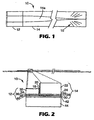
- Laser (10), aufweisend
einen Laserdiodenchip (12), der optisch mit einem passiven, sich verjüngenden Intrakavitäts-Wellenleiter (14a) gekoppelt ist, dadurch gekennzeichnet, dass der Laserdiodenchip eine Ausgangsöffnung einer Breite größer als 10 Mikrometer aufweist. - Laser (10) nach Anspruch 1, wobei der Laser (10) konfiguriert ist, eine einfache transversale Mode zu erzeugen.
- Laser nach Anspruch 1, wobei der Wellenleiter (14) einen kristallinen Werkstoff aufweist.
- Laser nach Anspruch 3, wobei der kristalline Werkstoff ein Einkristall ist.
- Laser nach Anspruch 3, wobei der kristalline Werkstoff einen II-VI-Verbindungshalbleiterwerkstoff aufweist.
- Laser nach Anspruch 5, wobei der II-VI-Verbindungshalbleiterwerkstoff BeZnTe aufweist.
- Laser nach Anspruch 1, wobei der Wellenleiter (14) ein Glas aufweist.
- Laser nach Anspruch 1, wobei der Laserdiodenchip (12) auf seiner Fläche an der Schnittstelle des Laserdiodenchips (12) und des Wellenleiters (14) eine Antireflexionsbeschichtung (18) aufweist.
- Laser nach Anspruch 1, wobei der Laserdiodenchip (12) und der Wellenleiter (14) jeder auf seiner Fläche an der Schnittstelle des Laserdiodenchips (12) und des Wellenleiters (14) eine Antireflexionsbeschichtung (18, 20) aufweisen.
- Laser nach Anspruch 1, wobei der Wellenleiter (14) eine Länge von 0,5 Zentimetern oder mehr aufweist.
- Optischer Verstärker, der den Laser (10) nach Anspruch 1 aufweist.
- Optischer Verstärker nach Anspruch 11, wobei der Verstärker mit einem Seltenerdmetall dotiert ist.
- Optischer Verstärker nach Anspruch 12, wobei der Verstärker mit Erbium dotiert ist.
- Optischer Verstärker nach Anspruch 13, wobei der Verstärker ferner mit Thulium dotiert ist.
- Optischer Verstärker nach Anspruch 11, wobei der Verstärker ein Raman-Verstärker ist.
- Optischer Verstärker nach Anspruch 13, wobei der Laser eine Ausgangsstrahl-Wellenlänge von etwa 980 nm oder etwa 1480 nm aufweist.
- Optischer Verstärker nach Anspruch 15, wobei der Laser eine Ausgangsstrahl-Wellenlänge von etwa 1365 nm bis etwa 1530 nm aufweist.
- Laserdrucksystem, das den Laser (10) nach Anspruch 1 aufweist.
- Lasersystem zur Erzeugung der zweiten Harmonischen, das den Laser (10) nach Anspruch 1 aufweist.
- Laser nach Anspruch 1, wobei der Laserdiodenchip (12) und der Wellenleiter (14) auf einer Unterbefestigung (44) ausgerichtet sind.
- Laser nach Anspruch 1, wobei der sich verjüngende Wellenleiter (14a) von ansteigender Sinuskontur ist.
Applications Claiming Priority (5)
| Application Number | Priority Date | Filing Date | Title |
|---|---|---|---|
| US30226801P | 2001-06-29 | 2001-06-29 | |
| US302268P | 2001-06-29 | ||
| US10/177,176 US6873638B2 (en) | 2001-06-29 | 2002-06-21 | Laser diode chip with waveguide |
| US177176 | 2002-06-21 | ||
| PCT/US2002/020344 WO2003003083A2 (en) | 2001-06-29 | 2002-06-25 | Laser diode chip with waveguide |
Publications (2)
| Publication Number | Publication Date |
|---|---|
| EP1402606A2 EP1402606A2 (de) | 2004-03-31 |
| EP1402606B1 true EP1402606B1 (de) | 2006-01-25 |
Family
ID=26873008
Family Applications (1)
| Application Number | Title | Priority Date | Filing Date |
|---|---|---|---|
| EP02749671A Expired - Lifetime EP1402606B1 (de) | 2001-06-29 | 2002-06-25 | Diodenlaserchip mit wellenleiter |
Country Status (9)
| Country | Link |
|---|---|
| US (1) | US6873638B2 (de) |
| EP (1) | EP1402606B1 (de) |
| JP (1) | JP4173806B2 (de) |
| KR (1) | KR100832381B1 (de) |
| CN (1) | CN1246942C (de) |
| AT (1) | ATE316701T1 (de) |
| AU (1) | AU2002320167A1 (de) |
| DE (1) | DE60208905T2 (de) |
| WO (1) | WO2003003083A2 (de) |
Families Citing this family (43)
| Publication number | Priority date | Publication date | Assignee | Title |
|---|---|---|---|---|
| US6941043B1 (en) * | 2001-07-10 | 2005-09-06 | K2 Optronics, Inc. | Wavelength stabilization of an external cavity laser diode (ECLD) |
| US6832034B2 (en) * | 2002-06-21 | 2004-12-14 | 3M Innovative Properties Company | Optical waveguide |
| WO2004038871A2 (en) * | 2002-08-22 | 2004-05-06 | Xponent Photonics Inc. | Grating-stabilized semiconductor laser |
| US7164837B2 (en) * | 2002-12-06 | 2007-01-16 | Agency For Science, Technology And Research | Method of fabricating optical waveguide devices with smooth and flat dielectric interfaces |
| US20050135725A1 (en) * | 2003-12-23 | 2005-06-23 | 3M Innovative Properties Company | Laser submounts with standoff structures |
| DE102004020454A1 (de) * | 2004-04-27 | 2005-11-24 | Heidelberger Druckmaschinen Ag | Vorrichtung zur Zuführung von Strahlungsenergie auf einen Bedruckstoff |
| US7119377B2 (en) * | 2004-06-18 | 2006-10-10 | 3M Innovative Properties Company | II-VI/III-V layered construction on InP substrate |
| US7126160B2 (en) * | 2004-06-18 | 2006-10-24 | 3M Innovative Properties Company | II-VI/III-V layered construction on InP substrate |
| US7173950B2 (en) * | 2004-06-25 | 2007-02-06 | Bookham Technology Plc | Low-noise high-power SHG laser system |
| US7508857B2 (en) * | 2004-12-14 | 2009-03-24 | Electronics And Telecommunications Research Institute | Semiconductor laser diode and method of manufacturing the same |
| KR100710048B1 (ko) | 2004-12-14 | 2007-04-23 | 한국전자통신연구원 | 반도체 레이저 다이오드 및 그 제조방법 |
| US20070084495A1 (en) * | 2005-10-14 | 2007-04-19 | Biprodas Dutta | Method for producing practical thermoelectric devices using quantum confinement in nanostructures |
| US20070084499A1 (en) * | 2005-10-14 | 2007-04-19 | Biprodas Dutta | Thermoelectric device produced by quantum confinement in nanostructures |
| RU2008127875A (ru) * | 2005-12-09 | 2010-01-20 | Конинклейке Филипс Электроникс Н.В. (Nl) | Оптически накачиваемый световодный лазер с улучшенной эффективностью |
| US7767564B2 (en) * | 2005-12-09 | 2010-08-03 | Zt3 Technologies, Inc. | Nanowire electronic devices and method for producing the same |
| US8658880B2 (en) * | 2005-12-09 | 2014-02-25 | Zt3 Technologies, Inc. | Methods of drawing wire arrays |
| US20070131269A1 (en) * | 2005-12-09 | 2007-06-14 | Biprodas Dutta | High density nanowire arrays in glassy matrix |
| US7559215B2 (en) * | 2005-12-09 | 2009-07-14 | Zt3 Technologies, Inc. | Methods of drawing high density nanowire arrays in a glassy matrix |
| KR101059331B1 (ko) * | 2006-02-22 | 2011-08-24 | 아이디 코포레이션 | 입력 클래딩 모드 흡수 구조 및/또는 출력 세그먼트 테이퍼구조를 갖는 저손실 깔대기형 피엘씨 광 스플리터 |
| US20080192794A1 (en) * | 2007-02-14 | 2008-08-14 | Jacob Meyer Hammer | Lateral-Bragg-Grating-Surface-Emitting Laser/Amplifier (LBGSE) |
| US20080310808A1 (en) * | 2007-06-18 | 2008-12-18 | International Business Machines Corporation | Photonic waveguide structure with planarized sidewall cladding layer |
| US7551826B2 (en) * | 2007-06-26 | 2009-06-23 | The University Of Connecticut | Integrated circuit employing low loss spot-size converter |
| JP5250245B2 (ja) * | 2007-11-21 | 2013-07-31 | 日本オクラロ株式会社 | 半導体レーザ |
| KR100958338B1 (ko) * | 2007-12-18 | 2010-05-17 | 한국전자통신연구원 | 광 증폭기가 집적된 슈퍼루미네슨트 다이오드 및 이를이용한 외부 공진 레이저 |
| US7693373B2 (en) * | 2007-12-18 | 2010-04-06 | Analog Devices, Inc. | Bidirectional optical link over a single multimode fiber or waveguide |
| CN102197551A (zh) * | 2008-09-04 | 2011-09-21 | 3M创新有限公司 | 由gan ld光泵的散热器上式ⅱ-ⅵ族mqw vcsel |
| WO2010027650A1 (en) * | 2008-09-04 | 2010-03-11 | 3M Innovative Properties Company | Light source with improved monochromaticity |
| JP2012502472A (ja) | 2008-09-04 | 2012-01-26 | スリーエム イノベイティブ プロパティズ カンパニー | 単色光源 |
| KR20110048580A (ko) * | 2008-09-04 | 2011-05-11 | 쓰리엠 이노베이티브 프로퍼티즈 컴파니 | 광 차단 구성요소를 갖는 광원 |
| CN101907754A (zh) * | 2010-07-09 | 2010-12-08 | 浙江大学 | 一种用于半导体激光器的波导耦合器芯片 |
| JP2012248812A (ja) * | 2011-05-31 | 2012-12-13 | Sumitomo Electric Ind Ltd | 半導体光集積素子の製造方法 |
| US9658396B2 (en) * | 2011-09-29 | 2017-05-23 | Intel Corporation | Vertical optical coupler for planar photonic circuits |
| WO2013093905A1 (en) * | 2011-12-23 | 2013-06-27 | Technion Research & Development Foundation Ltd. | Fiber optical superconducting nanowire single photon detector |
| US8681594B1 (en) | 2012-09-28 | 2014-03-25 | Western Digital (Fremont), Llc | Method and system for improving laser alignment and optical transmission efficiency of an energy assisted magnetic recording head |
| CN104184046B (zh) * | 2014-08-29 | 2017-01-25 | 清华大学 | 用于半导体激光器与TriPleX波导耦合的耦合结构及制备方法 |
| CN105445854B (zh) * | 2015-11-06 | 2018-09-25 | 南京邮电大学 | 硅衬底悬空led光波导集成光子器件及其制备方法 |
| US10020635B1 (en) | 2016-04-15 | 2018-07-10 | University Of Central Florida Research Foundation, Inc. | Spectrometer device with stabilized laser and related devices and methods |
| US10355449B2 (en) | 2016-08-15 | 2019-07-16 | University Of Central Florida Research Foundation, Inc. | Quantum cascade laser with angled active region and related methods |
| FR3060772B1 (fr) * | 2016-12-20 | 2022-12-30 | Thales Sa | Circuit photonique integre optimise |
| CN108899760B (zh) * | 2018-07-12 | 2020-06-09 | 中国科学院长春光学精密机械与物理研究所 | 一种半导体激光器及制作方法 |
| CN110749955A (zh) * | 2018-07-23 | 2020-02-04 | 上海新微技术研发中心有限公司 | 光波模式转换装置及其制造方法 |
| WO2020096950A1 (en) * | 2018-11-06 | 2020-05-14 | The Regents Of The University Of California | Heterogeneously integrated indium gallium nitride on silicon photonic integrated circuits |
| US20230092838A1 (en) * | 2021-09-23 | 2023-03-23 | Osram Opto Semiconductors Gmbh | Optoelectronic semiconductor device and glasses |
Family Cites Families (23)
| Publication number | Priority date | Publication date | Assignee | Title |
|---|---|---|---|---|
| US4875216A (en) * | 1987-11-30 | 1989-10-17 | Xerox Corporation | Buried waveguide window regions for improved performance semiconductor lasers and other opto-electronic applications |
| US5144634A (en) | 1989-09-07 | 1992-09-01 | International Business Machines Corporation | Method for mirror passivation of semiconductor laser diodes |
| US5585957A (en) * | 1993-03-25 | 1996-12-17 | Nippon Telegraph And Telephone Corporation | Method for producing various semiconductor optical devices of differing optical characteristics |
| US5613995A (en) | 1993-04-23 | 1997-03-25 | Lucent Technologies Inc. | Method for making planar optical waveguides |
| US5389396A (en) | 1993-08-11 | 1995-02-14 | Northwestern University | InGaAsP/GaAs diode laser |
| US5574742A (en) | 1994-05-31 | 1996-11-12 | Lucent Technologies Inc. | Tapered beam expander waveguide integrated with a diode laser |
| EP1315006A1 (de) * | 1994-06-22 | 2003-05-28 | Fujitsu Limited | Verfahren zur Herstellung von Wellenleitersystemen, dessen Verwendung in optischem Bauelement und Koppler sowie optisches Netzwerk und optische Leiterplatte |
| US5764842A (en) * | 1995-03-23 | 1998-06-09 | Hitachi, Ltd. | Semiconductor guided-wave optical device and method of fabricating thereof |
| US5879962A (en) | 1995-12-13 | 1999-03-09 | Minnesota Mining And Manufacturing Company | III-V/II-VI Semiconductor interface fabrication method |
| FR2747192B1 (fr) * | 1996-04-04 | 1998-04-30 | Commissariat Energie Atomique | Dispositif de detection de gaz a distance comportant un microlaser |
| DE19626113A1 (de) * | 1996-06-28 | 1998-01-02 | Sel Alcatel Ag | Optisches Halbleiterbauelement mit tiefem Rippenwellenleiter |
| DE19626130A1 (de) * | 1996-06-28 | 1998-01-08 | Sel Alcatel Ag | Optisches Halbleiterbauelement mit tiefem Rippenwellenleiter |
| JPH1048789A (ja) * | 1996-08-02 | 1998-02-20 | Fuji Photo Film Co Ltd | ハロゲン化銀カラー写真感光材料の処理方法 |
| DE19652533C1 (de) * | 1996-12-17 | 1998-04-30 | Siemens Ag | Optoelektronischer Modul |
| US5870417A (en) | 1996-12-20 | 1999-02-09 | Sdl, Inc. | Thermal compensators for waveguide DBR laser sources |
| DE69704074T2 (de) * | 1997-03-27 | 2001-06-21 | Tno | Erbiumdotierter planarer Wellenleiter |
| US6087725A (en) * | 1997-09-29 | 2000-07-11 | Matsushita Electric Industrial Co., Ltd. | Low barrier ohmic contact for semiconductor light emitting device |
| US6052397A (en) * | 1997-12-05 | 2000-04-18 | Sdl, Inc. | Laser diode device having a substantially circular light output beam and a method of forming a tapered section in a semiconductor device to provide for a reproducible mode profile of the output beam |
| US6160660A (en) * | 1997-12-31 | 2000-12-12 | Pirelli Cavi E Sistemi S.P.A. | Bidirectional optical transmission system for dense interleaved wavelength division multiplexing |
| JPH11218641A (ja) | 1998-02-04 | 1999-08-10 | Furukawa Electric Co Ltd:The | レンズ付き光ファイバとレーザモジュール |
| US6137117A (en) * | 1999-06-21 | 2000-10-24 | The United States Of America As Represented By The Secretary Of The Navy | Integrating multi-waveguide sensor |
| US6312581B1 (en) | 1999-11-30 | 2001-11-06 | Agere Systems Optoelectronics Guardian Corp. | Process for fabricating an optical device |
| US6580850B1 (en) | 2000-11-24 | 2003-06-17 | Applied Wdm, Inc. | Optical waveguide multimode to single mode transformer |
-
2002
- 2002-06-21 US US10/177,176 patent/US6873638B2/en not_active Expired - Lifetime
- 2002-06-25 AT AT02749671T patent/ATE316701T1/de not_active IP Right Cessation
- 2002-06-25 JP JP2003509207A patent/JP4173806B2/ja not_active Expired - Fee Related
- 2002-06-25 DE DE60208905T patent/DE60208905T2/de not_active Expired - Lifetime
- 2002-06-25 KR KR1020037017135A patent/KR100832381B1/ko active IP Right Grant
- 2002-06-25 AU AU2002320167A patent/AU2002320167A1/en not_active Abandoned
- 2002-06-25 CN CNB028131673A patent/CN1246942C/zh not_active Expired - Fee Related
- 2002-06-25 WO PCT/US2002/020344 patent/WO2003003083A2/en active IP Right Grant
- 2002-06-25 EP EP02749671A patent/EP1402606B1/de not_active Expired - Lifetime
Also Published As
| Publication number | Publication date |
|---|---|
| ATE316701T1 (de) | 2006-02-15 |
| WO2003003083A2 (en) | 2003-01-09 |
| CN1524325A (zh) | 2004-08-25 |
| KR100832381B1 (ko) | 2008-05-26 |
| JP2004531904A (ja) | 2004-10-14 |
| KR20040013000A (ko) | 2004-02-11 |
| WO2003003083A3 (en) | 2003-08-14 |
| AU2002320167A1 (en) | 2003-03-03 |
| CN1246942C (zh) | 2006-03-22 |
| JP4173806B2 (ja) | 2008-10-29 |
| DE60208905T2 (de) | 2006-08-10 |
| US6873638B2 (en) | 2005-03-29 |
| DE60208905D1 (de) | 2006-04-13 |
| EP1402606A2 (de) | 2004-03-31 |
| US20030007535A1 (en) | 2003-01-09 |
Similar Documents
| Publication | Publication Date | Title |
|---|---|---|
| EP1402606B1 (de) | Diodenlaserchip mit wellenleiter | |
| Spott et al. | Heterogeneous integration for mid-infrared silicon photonics | |
| US6625182B1 (en) | Semiconductor or solid-state laser having an external fiber cavity | |
| JP5717726B2 (ja) | 大出力パワー用の横結合を持つdfbレーザダイオード | |
| Huang et al. | High-power nearly diffraction-limited AlGaAs-InGaAs semiconductor slab-coupled optical waveguide laser | |
| EP1248335B1 (de) | Nitrid-Halbleiterlaservorrichtung und deren Herstellungsverfahren | |
| Shigihara et al. | High-power 980-nm ridge waveguide laser diodes including an asymmetrically expanded optical field normal to the active layer | |
| JP2002141611A (ja) | 半導体発光素子およびその製造方法 | |
| JP4027801B2 (ja) | 光学装置のヒートシンク上への取り付け | |
| JP2967757B2 (ja) | 半導体レーザ装置及びその製造方法 | |
| Kallenbach et al. | High-power high-brightness ridge-waveguide tapered diode lasers at 14xx nm | |
| Harder | Pump diode lasers | |
| Ryu et al. | 1.55-μm spot-size converter integrated laser diode with conventional buried-heterostructure laser process | |
| Robertson et al. | The Expanded Mode Laser< cd0215d. gif> A Route to Low Cost Optoelectronics | |
| Chang et al. | Stable single-mode operation of VCSELs with a mode selective aperture | |
| JP2008211260A (ja) | 半導体レーザ及びその製造方法 | |
| JP2001148541A (ja) | 半導体発光装置およびその半導体発光装置を励起光源に用いた固体レーザ装置 | |
| US6455341B1 (en) | Increasing the yield of precise wavelength lasers | |
| Gough et al. | Low-divergence laser structures for cost-effective fiber coupling applications | |
| Hardwell | Solid-state lasers: properties and applications | |
| Tohmori et al. | 1.3-/spl mu/m spot-size converter integrated laser diodes (SS-LDs) for access network applications | |
| Broeke et al. | Monolithical integration of semiconductor optical amplifiers and passive modefilters for low facet reflectivity | |
| Swint et al. | High power single lateral mode buried ridge laser incorporating a curved waveguide for spatial filtering | |
| Walpole et al. | High-power 1.3 um InGaAsP/InP lasers and amplifiers with tapered gain regions | |
| JP2000244064A (ja) | 半導体レーザ直接結合型光導波路素子 |
Legal Events
| Date | Code | Title | Description |
|---|---|---|---|
| PUAI | Public reference made under article 153(3) epc to a published international application that has entered the european phase |
Free format text: ORIGINAL CODE: 0009012 |
|
| 17P | Request for examination filed |
Effective date: 20031219 |
|
| AK | Designated contracting states |
Kind code of ref document: A2 Designated state(s): AT BE CH CY DE DK ES FI FR GB GR IE IT LI LU MC NL PT SE TR |
|
| AX | Request for extension of the european patent |
Extension state: AL LT LV MK RO SI |
|
| GRAP | Despatch of communication of intention to grant a patent |
Free format text: ORIGINAL CODE: EPIDOSNIGR1 |
|
| GRAS | Grant fee paid |
Free format text: ORIGINAL CODE: EPIDOSNIGR3 |
|
| GRAA | (expected) grant |
Free format text: ORIGINAL CODE: 0009210 |
|
| AK | Designated contracting states |
Kind code of ref document: B1 Designated state(s): AT BE CH CY DE DK ES FI FR GB GR IE IT LI LU MC NL PT SE TR |
|
| PG25 | Lapsed in a contracting state [announced via postgrant information from national office to epo] |
Ref country code: IT Free format text: LAPSE BECAUSE OF FAILURE TO SUBMIT A TRANSLATION OF THE DESCRIPTION OR TO PAY THE FEE WITHIN THE PRESCRIBED TIME-LIMIT;WARNING: LAPSES OF ITALIAN PATENTS WITH EFFECTIVE DATE BEFORE 2007 MAY HAVE OCCURRED AT ANY TIME BEFORE 2007. THE CORRECT EFFECTIVE DATE MAY BE DIFFERENT FROM THE ONE RECORDED. Effective date: 20060125 Ref country code: AT Free format text: LAPSE BECAUSE OF FAILURE TO SUBMIT A TRANSLATION OF THE DESCRIPTION OR TO PAY THE FEE WITHIN THE PRESCRIBED TIME-LIMIT Effective date: 20060125 Ref country code: BE Free format text: LAPSE BECAUSE OF FAILURE TO SUBMIT A TRANSLATION OF THE DESCRIPTION OR TO PAY THE FEE WITHIN THE PRESCRIBED TIME-LIMIT Effective date: 20060125 Ref country code: NL Free format text: LAPSE BECAUSE OF FAILURE TO SUBMIT A TRANSLATION OF THE DESCRIPTION OR TO PAY THE FEE WITHIN THE PRESCRIBED TIME-LIMIT Effective date: 20060125 Ref country code: CH Free format text: LAPSE BECAUSE OF FAILURE TO SUBMIT A TRANSLATION OF THE DESCRIPTION OR TO PAY THE FEE WITHIN THE PRESCRIBED TIME-LIMIT Effective date: 20060125 Ref country code: FI Free format text: LAPSE BECAUSE OF FAILURE TO SUBMIT A TRANSLATION OF THE DESCRIPTION OR TO PAY THE FEE WITHIN THE PRESCRIBED TIME-LIMIT Effective date: 20060125 Ref country code: LI Free format text: LAPSE BECAUSE OF FAILURE TO SUBMIT A TRANSLATION OF THE DESCRIPTION OR TO PAY THE FEE WITHIN THE PRESCRIBED TIME-LIMIT Effective date: 20060125 |
|
| REG | Reference to a national code |
Ref country code: GB Ref legal event code: FG4D |
|
| REG | Reference to a national code |
Ref country code: CH Ref legal event code: EP |
|
| REG | Reference to a national code |
Ref country code: IE Ref legal event code: FG4D |
|
| REF | Corresponds to: |
Ref document number: 60208905 Country of ref document: DE Date of ref document: 20060413 Kind code of ref document: P |
|
| PG25 | Lapsed in a contracting state [announced via postgrant information from national office to epo] |
Ref country code: SE Free format text: LAPSE BECAUSE OF FAILURE TO SUBMIT A TRANSLATION OF THE DESCRIPTION OR TO PAY THE FEE WITHIN THE PRESCRIBED TIME-LIMIT Effective date: 20060425 Ref country code: DK Free format text: LAPSE BECAUSE OF FAILURE TO SUBMIT A TRANSLATION OF THE DESCRIPTION OR TO PAY THE FEE WITHIN THE PRESCRIBED TIME-LIMIT Effective date: 20060425 |
|
| PG25 | Lapsed in a contracting state [announced via postgrant information from national office to epo] |
Ref country code: ES Free format text: LAPSE BECAUSE OF FAILURE TO SUBMIT A TRANSLATION OF THE DESCRIPTION OR TO PAY THE FEE WITHIN THE PRESCRIBED TIME-LIMIT Effective date: 20060506 |
|
| PG25 | Lapsed in a contracting state [announced via postgrant information from national office to epo] |
Ref country code: IE Free format text: LAPSE BECAUSE OF NON-PAYMENT OF DUE FEES Effective date: 20060626 Ref country code: PT Free format text: LAPSE BECAUSE OF FAILURE TO SUBMIT A TRANSLATION OF THE DESCRIPTION OR TO PAY THE FEE WITHIN THE PRESCRIBED TIME-LIMIT Effective date: 20060626 |
|
| PG25 | Lapsed in a contracting state [announced via postgrant information from national office to epo] |
Ref country code: MC Free format text: LAPSE BECAUSE OF NON-PAYMENT OF DUE FEES Effective date: 20060630 |
|
| NLV1 | Nl: lapsed or annulled due to failure to fulfill the requirements of art. 29p and 29m of the patents act | ||
| REG | Reference to a national code |
Ref country code: CH Ref legal event code: PL |
|
| PLBE | No opposition filed within time limit |
Free format text: ORIGINAL CODE: 0009261 |
|
| STAA | Information on the status of an ep patent application or granted ep patent |
Free format text: STATUS: NO OPPOSITION FILED WITHIN TIME LIMIT |
|
| 26N | No opposition filed |
Effective date: 20061026 |
|
| PGFP | Annual fee paid to national office [announced via postgrant information from national office to epo] |
Ref country code: GB Payment date: 20070628 Year of fee payment: 6 |
|
| PG25 | Lapsed in a contracting state [announced via postgrant information from national office to epo] |
Ref country code: FR Free format text: LAPSE BECAUSE OF FAILURE TO SUBMIT A TRANSLATION OF THE DESCRIPTION OR TO PAY THE FEE WITHIN THE PRESCRIBED TIME-LIMIT Effective date: 20070316 Ref country code: GR Free format text: LAPSE BECAUSE OF FAILURE TO SUBMIT A TRANSLATION OF THE DESCRIPTION OR TO PAY THE FEE WITHIN THE PRESCRIBED TIME-LIMIT Effective date: 20060426 |
|
| PG25 | Lapsed in a contracting state [announced via postgrant information from national office to epo] |
Ref country code: LU Free format text: LAPSE BECAUSE OF NON-PAYMENT OF DUE FEES Effective date: 20060625 Ref country code: TR Free format text: LAPSE BECAUSE OF FAILURE TO SUBMIT A TRANSLATION OF THE DESCRIPTION OR TO PAY THE FEE WITHIN THE PRESCRIBED TIME-LIMIT Effective date: 20060125 |
|
| PG25 | Lapsed in a contracting state [announced via postgrant information from national office to epo] |
Ref country code: FR Free format text: LAPSE BECAUSE OF FAILURE TO SUBMIT A TRANSLATION OF THE DESCRIPTION OR TO PAY THE FEE WITHIN THE PRESCRIBED TIME-LIMIT Effective date: 20060125 Ref country code: CY Free format text: LAPSE BECAUSE OF FAILURE TO SUBMIT A TRANSLATION OF THE DESCRIPTION OR TO PAY THE FEE WITHIN THE PRESCRIBED TIME-LIMIT Effective date: 20060125 |
|
| GBPC | Gb: european patent ceased through non-payment of renewal fee |
Effective date: 20080625 |
|
| PG25 | Lapsed in a contracting state [announced via postgrant information from national office to epo] |
Ref country code: GB Free format text: LAPSE BECAUSE OF NON-PAYMENT OF DUE FEES Effective date: 20080625 |
|
| PGFP | Annual fee paid to national office [announced via postgrant information from national office to epo] |
Ref country code: DE Payment date: 20160622 Year of fee payment: 15 |
|
| REG | Reference to a national code |
Ref country code: DE Ref legal event code: R119 Ref document number: 60208905 Country of ref document: DE |
|
| PG25 | Lapsed in a contracting state [announced via postgrant information from national office to epo] |
Ref country code: DE Free format text: LAPSE BECAUSE OF NON-PAYMENT OF DUE FEES Effective date: 20180103 |