EP1401020A1 - Semiconductor device and manufacturing method thereof - Google Patents
Semiconductor device and manufacturing method thereof Download PDFInfo
- Publication number
- EP1401020A1 EP1401020A1 EP02714493A EP02714493A EP1401020A1 EP 1401020 A1 EP1401020 A1 EP 1401020A1 EP 02714493 A EP02714493 A EP 02714493A EP 02714493 A EP02714493 A EP 02714493A EP 1401020 A1 EP1401020 A1 EP 1401020A1
- Authority
- EP
- European Patent Office
- Prior art keywords
- semiconductor chip
- main surface
- wiring substrate
- semiconductor
- plural
- Prior art date
- Legal status (The legal status is an assumption and is not a legal conclusion. Google has not performed a legal analysis and makes no representation as to the accuracy of the status listed.)
- Withdrawn
Links
Images














Classifications
-
- H—ELECTRICITY
- H10—SEMICONDUCTOR DEVICES; ELECTRIC SOLID-STATE DEVICES NOT OTHERWISE PROVIDED FOR
- H10W—GENERIC PACKAGES, INTERCONNECTIONS, CONNECTORS OR OTHER CONSTRUCTIONAL DETAILS OF DEVICES COVERED BY CLASS H10
- H10W70/00—Package substrates; Interposers; Redistribution layers [RDL]
- H10W70/60—Insulating or insulated package substrates; Interposers; Redistribution layers
-
- H—ELECTRICITY
- H10—SEMICONDUCTOR DEVICES; ELECTRIC SOLID-STATE DEVICES NOT OTHERWISE PROVIDED FOR
- H10W—GENERIC PACKAGES, INTERCONNECTIONS, CONNECTORS OR OTHER CONSTRUCTIONAL DETAILS OF DEVICES COVERED BY CLASS H10
- H10W70/00—Package substrates; Interposers; Redistribution layers [RDL]
- H10W70/60—Insulating or insulated package substrates; Interposers; Redistribution layers
- H10W70/611—Insulating or insulated package substrates; Interposers; Redistribution layers for connecting multiple chips together
-
- H—ELECTRICITY
- H10—SEMICONDUCTOR DEVICES; ELECTRIC SOLID-STATE DEVICES NOT OTHERWISE PROVIDED FOR
- H10W—GENERIC PACKAGES, INTERCONNECTIONS, CONNECTORS OR OTHER CONSTRUCTIONAL DETAILS OF DEVICES COVERED BY CLASS H10
- H10W70/00—Package substrates; Interposers; Redistribution layers [RDL]
- H10W70/60—Insulating or insulated package substrates; Interposers; Redistribution layers
- H10W70/62—Insulating or insulated package substrates; Interposers; Redistribution layers characterised by their interconnections
- H10W70/65—Shapes or dispositions of interconnections
-
- H—ELECTRICITY
- H10—SEMICONDUCTOR DEVICES; ELECTRIC SOLID-STATE DEVICES NOT OTHERWISE PROVIDED FOR
- H10W—GENERIC PACKAGES, INTERCONNECTIONS, CONNECTORS OR OTHER CONSTRUCTIONAL DETAILS OF DEVICES COVERED BY CLASS H10
- H10W72/00—Interconnections or connectors in packages
-
- H—ELECTRICITY
- H10—SEMICONDUCTOR DEVICES; ELECTRIC SOLID-STATE DEVICES NOT OTHERWISE PROVIDED FOR
- H10W—GENERIC PACKAGES, INTERCONNECTIONS, CONNECTORS OR OTHER CONSTRUCTIONAL DETAILS OF DEVICES COVERED BY CLASS H10
- H10W74/00—Encapsulations, e.g. protective coatings
-
- H—ELECTRICITY
- H10—SEMICONDUCTOR DEVICES; ELECTRIC SOLID-STATE DEVICES NOT OTHERWISE PROVIDED FOR
- H10W—GENERIC PACKAGES, INTERCONNECTIONS, CONNECTORS OR OTHER CONSTRUCTIONAL DETAILS OF DEVICES COVERED BY CLASS H10
- H10W74/00—Encapsulations, e.g. protective coatings
- H10W74/10—Encapsulations, e.g. protective coatings characterised by their shape or disposition
- H10W74/111—Encapsulations, e.g. protective coatings characterised by their shape or disposition the semiconductor body being completely enclosed
- H10W74/114—Encapsulations, e.g. protective coatings characterised by their shape or disposition the semiconductor body being completely enclosed by a substrate and the encapsulations
- H10W74/117—Encapsulations, e.g. protective coatings characterised by their shape or disposition the semiconductor body being completely enclosed by a substrate and the encapsulations the substrate having spherical bumps for external connection
-
- H—ELECTRICITY
- H10—SEMICONDUCTOR DEVICES; ELECTRIC SOLID-STATE DEVICES NOT OTHERWISE PROVIDED FOR
- H10W—GENERIC PACKAGES, INTERCONNECTIONS, CONNECTORS OR OTHER CONSTRUCTIONAL DETAILS OF DEVICES COVERED BY CLASS H10
- H10W90/00—Package configurations
-
- H—ELECTRICITY
- H10—SEMICONDUCTOR DEVICES; ELECTRIC SOLID-STATE DEVICES NOT OTHERWISE PROVIDED FOR
- H10W—GENERIC PACKAGES, INTERCONNECTIONS, CONNECTORS OR OTHER CONSTRUCTIONAL DETAILS OF DEVICES COVERED BY CLASS H10
- H10W70/00—Package substrates; Interposers; Redistribution layers [RDL]
- H10W70/60—Insulating or insulated package substrates; Interposers; Redistribution layers
- H10W70/62—Insulating or insulated package substrates; Interposers; Redistribution layers characterised by their interconnections
- H10W70/65—Shapes or dispositions of interconnections
- H10W70/654—Top-view layouts
- H10W70/655—Fan-out layouts
-
- H—ELECTRICITY
- H10—SEMICONDUCTOR DEVICES; ELECTRIC SOLID-STATE DEVICES NOT OTHERWISE PROVIDED FOR
- H10W—GENERIC PACKAGES, INTERCONNECTIONS, CONNECTORS OR OTHER CONSTRUCTIONAL DETAILS OF DEVICES COVERED BY CLASS H10
- H10W72/00—Interconnections or connectors in packages
- H10W72/01—Manufacture or treatment
- H10W72/012—Manufacture or treatment of bump connectors, dummy bumps or thermal bumps
- H10W72/01221—Manufacture or treatment of bump connectors, dummy bumps or thermal bumps using local deposition
- H10W72/01225—Manufacture or treatment of bump connectors, dummy bumps or thermal bumps using local deposition in solid form, e.g. by using a powder or by stud bumping
-
- H—ELECTRICITY
- H10—SEMICONDUCTOR DEVICES; ELECTRIC SOLID-STATE DEVICES NOT OTHERWISE PROVIDED FOR
- H10W—GENERIC PACKAGES, INTERCONNECTIONS, CONNECTORS OR OTHER CONSTRUCTIONAL DETAILS OF DEVICES COVERED BY CLASS H10
- H10W72/00—Interconnections or connectors in packages
- H10W72/01—Manufacture or treatment
- H10W72/0198—Manufacture or treatment batch processes
-
- H—ELECTRICITY
- H10—SEMICONDUCTOR DEVICES; ELECTRIC SOLID-STATE DEVICES NOT OTHERWISE PROVIDED FOR
- H10W—GENERIC PACKAGES, INTERCONNECTIONS, CONNECTORS OR OTHER CONSTRUCTIONAL DETAILS OF DEVICES COVERED BY CLASS H10
- H10W72/00—Interconnections or connectors in packages
- H10W72/071—Connecting or disconnecting
- H10W72/072—Connecting or disconnecting of bump connectors
- H10W72/07251—Connecting or disconnecting of bump connectors characterised by changes in properties of the bump connectors during connecting
-
- H—ELECTRICITY
- H10—SEMICONDUCTOR DEVICES; ELECTRIC SOLID-STATE DEVICES NOT OTHERWISE PROVIDED FOR
- H10W—GENERIC PACKAGES, INTERCONNECTIONS, CONNECTORS OR OTHER CONSTRUCTIONAL DETAILS OF DEVICES COVERED BY CLASS H10
- H10W72/00—Interconnections or connectors in packages
- H10W72/20—Bump connectors, e.g. solder bumps or copper pillars; Dummy bumps; Thermal bumps
-
- H—ELECTRICITY
- H10—SEMICONDUCTOR DEVICES; ELECTRIC SOLID-STATE DEVICES NOT OTHERWISE PROVIDED FOR
- H10W—GENERIC PACKAGES, INTERCONNECTIONS, CONNECTORS OR OTHER CONSTRUCTIONAL DETAILS OF DEVICES COVERED BY CLASS H10
- H10W72/00—Interconnections or connectors in packages
- H10W72/20—Bump connectors, e.g. solder bumps or copper pillars; Dummy bumps; Thermal bumps
- H10W72/251—Materials
- H10W72/252—Materials comprising solid metals or solid metalloids, e.g. PbSn, Ag or Cu
-
- H—ELECTRICITY
- H10—SEMICONDUCTOR DEVICES; ELECTRIC SOLID-STATE DEVICES NOT OTHERWISE PROVIDED FOR
- H10W—GENERIC PACKAGES, INTERCONNECTIONS, CONNECTORS OR OTHER CONSTRUCTIONAL DETAILS OF DEVICES COVERED BY CLASS H10
- H10W72/00—Interconnections or connectors in packages
- H10W72/50—Bond wires
- H10W72/531—Shapes of wire connectors
- H10W72/536—Shapes of wire connectors the connected ends being ball-shaped
-
- H—ELECTRICITY
- H10—SEMICONDUCTOR DEVICES; ELECTRIC SOLID-STATE DEVICES NOT OTHERWISE PROVIDED FOR
- H10W—GENERIC PACKAGES, INTERCONNECTIONS, CONNECTORS OR OTHER CONSTRUCTIONAL DETAILS OF DEVICES COVERED BY CLASS H10
- H10W72/00—Interconnections or connectors in packages
- H10W72/50—Bond wires
- H10W72/531—Shapes of wire connectors
- H10W72/5363—Shapes of wire connectors the connected ends being wedge-shaped
-
- H—ELECTRICITY
- H10—SEMICONDUCTOR DEVICES; ELECTRIC SOLID-STATE DEVICES NOT OTHERWISE PROVIDED FOR
- H10W—GENERIC PACKAGES, INTERCONNECTIONS, CONNECTORS OR OTHER CONSTRUCTIONAL DETAILS OF DEVICES COVERED BY CLASS H10
- H10W72/00—Interconnections or connectors in packages
- H10W72/50—Bond wires
- H10W72/541—Dispositions of bond wires
- H10W72/5449—Dispositions of bond wires not being orthogonal to a side surface of the chip, e.g. fan-out arrangements
-
- H—ELECTRICITY
- H10—SEMICONDUCTOR DEVICES; ELECTRIC SOLID-STATE DEVICES NOT OTHERWISE PROVIDED FOR
- H10W—GENERIC PACKAGES, INTERCONNECTIONS, CONNECTORS OR OTHER CONSTRUCTIONAL DETAILS OF DEVICES COVERED BY CLASS H10
- H10W72/00—Interconnections or connectors in packages
- H10W72/50—Bond wires
- H10W72/551—Materials of bond wires
- H10W72/552—Materials of bond wires comprising metals or metalloids, e.g. silver
- H10W72/5522—Materials of bond wires comprising metals or metalloids, e.g. silver comprising gold [Au]
-
- H—ELECTRICITY
- H10—SEMICONDUCTOR DEVICES; ELECTRIC SOLID-STATE DEVICES NOT OTHERWISE PROVIDED FOR
- H10W—GENERIC PACKAGES, INTERCONNECTIONS, CONNECTORS OR OTHER CONSTRUCTIONAL DETAILS OF DEVICES COVERED BY CLASS H10
- H10W72/00—Interconnections or connectors in packages
- H10W72/851—Dispositions of multiple connectors or interconnections
- H10W72/874—On different surfaces
- H10W72/877—Bump connectors and die-attach connectors
-
- H—ELECTRICITY
- H10—SEMICONDUCTOR DEVICES; ELECTRIC SOLID-STATE DEVICES NOT OTHERWISE PROVIDED FOR
- H10W—GENERIC PACKAGES, INTERCONNECTIONS, CONNECTORS OR OTHER CONSTRUCTIONAL DETAILS OF DEVICES COVERED BY CLASS H10
- H10W72/00—Interconnections or connectors in packages
- H10W72/851—Dispositions of multiple connectors or interconnections
- H10W72/874—On different surfaces
- H10W72/884—Die-attach connectors and bond wires
-
- H—ELECTRICITY
- H10—SEMICONDUCTOR DEVICES; ELECTRIC SOLID-STATE DEVICES NOT OTHERWISE PROVIDED FOR
- H10W—GENERIC PACKAGES, INTERCONNECTIONS, CONNECTORS OR OTHER CONSTRUCTIONAL DETAILS OF DEVICES COVERED BY CLASS H10
- H10W74/00—Encapsulations, e.g. protective coatings
- H10W74/10—Encapsulations, e.g. protective coatings characterised by their shape or disposition
- H10W74/15—Encapsulations, e.g. protective coatings characterised by their shape or disposition on active surfaces of flip-chip devices, e.g. underfills
-
- H—ELECTRICITY
- H10—SEMICONDUCTOR DEVICES; ELECTRIC SOLID-STATE DEVICES NOT OTHERWISE PROVIDED FOR
- H10W—GENERIC PACKAGES, INTERCONNECTIONS, CONNECTORS OR OTHER CONSTRUCTIONAL DETAILS OF DEVICES COVERED BY CLASS H10
- H10W90/00—Package configurations
- H10W90/20—Configurations of stacked chips
- H10W90/271—Configurations of stacked chips the chips having passive surfaces facing each other, i.e. in a back-to-back arrangement
-
- H—ELECTRICITY
- H10—SEMICONDUCTOR DEVICES; ELECTRIC SOLID-STATE DEVICES NOT OTHERWISE PROVIDED FOR
- H10W—GENERIC PACKAGES, INTERCONNECTIONS, CONNECTORS OR OTHER CONSTRUCTIONAL DETAILS OF DEVICES COVERED BY CLASS H10
- H10W90/00—Package configurations
- H10W90/701—Package configurations characterised by the relative positions of pads or connectors relative to package parts
- H10W90/721—Package configurations characterised by the relative positions of pads or connectors relative to package parts of bump connectors
- H10W90/724—Package configurations characterised by the relative positions of pads or connectors relative to package parts of bump connectors between a chip and a stacked insulating package substrate, interposer or RDL
-
- H—ELECTRICITY
- H10—SEMICONDUCTOR DEVICES; ELECTRIC SOLID-STATE DEVICES NOT OTHERWISE PROVIDED FOR
- H10W—GENERIC PACKAGES, INTERCONNECTIONS, CONNECTORS OR OTHER CONSTRUCTIONAL DETAILS OF DEVICES COVERED BY CLASS H10
- H10W90/00—Package configurations
- H10W90/701—Package configurations characterised by the relative positions of pads or connectors relative to package parts
- H10W90/731—Package configurations characterised by the relative positions of pads or connectors relative to package parts of die-attach connectors
- H10W90/732—Package configurations characterised by the relative positions of pads or connectors relative to package parts of die-attach connectors between stacked chips
-
- H—ELECTRICITY
- H10—SEMICONDUCTOR DEVICES; ELECTRIC SOLID-STATE DEVICES NOT OTHERWISE PROVIDED FOR
- H10W—GENERIC PACKAGES, INTERCONNECTIONS, CONNECTORS OR OTHER CONSTRUCTIONAL DETAILS OF DEVICES COVERED BY CLASS H10
- H10W90/00—Package configurations
- H10W90/701—Package configurations characterised by the relative positions of pads or connectors relative to package parts
- H10W90/731—Package configurations characterised by the relative positions of pads or connectors relative to package parts of die-attach connectors
- H10W90/734—Package configurations characterised by the relative positions of pads or connectors relative to package parts of die-attach connectors between a chip and a stacked insulating package substrate, interposer or RDL
-
- H—ELECTRICITY
- H10—SEMICONDUCTOR DEVICES; ELECTRIC SOLID-STATE DEVICES NOT OTHERWISE PROVIDED FOR
- H10W—GENERIC PACKAGES, INTERCONNECTIONS, CONNECTORS OR OTHER CONSTRUCTIONAL DETAILS OF DEVICES COVERED BY CLASS H10
- H10W90/00—Package configurations
- H10W90/701—Package configurations characterised by the relative positions of pads or connectors relative to package parts
- H10W90/751—Package configurations characterised by the relative positions of pads or connectors relative to package parts of bond wires
- H10W90/754—Package configurations characterised by the relative positions of pads or connectors relative to package parts of bond wires between a chip and a stacked insulating package substrate, interposer or RDL
Definitions
- the present invention relates to a semiconductor device and a method of manufacturing the same. Particularly, the present invention is concerned with a technique applicable effectively to a multi-chip module (MCM) or a mutli-chip package (MCP) wherein plural semiconductor chips are mounted on one and same wiring substrate.
- MCM multi-chip module
- MCP mutli-chip package
- Japanese Unexamined Patent Publication No. Hei 4(1992)-302164 discloses a package structure wherein plural semiconductor chips having the same function and the same size are stacked in the shape of stairs through insulating layers, and bonding pads exposed to the stair portion of each semiconductor chip are electrically connected to inner leads of a package through wires.
- Japanese Unexamined Patent Publication No. Hei 11(1999)-204720 there is disclosed a package structure wherein a first semiconductor chip is mounted on an insulating substrate through a thermocompression-bonded sheet, a second semiconductor chip smaller in external size than the first semiconductor chip is mounted on the first semiconductor chip through a thermocompression-bonded sheet, bonding pads on the first and second semiconductor chips and a wiring layer on the insulating substrate are electrically connected with each other through wires, and the first and second semiconductor chips and the wires are sealed with resin.
- the inventors in the present case are developing a multi-chip module wherein plural semiconductor chips (hereinafter referred to simply as "chips") are mounted within a single package.
- a chip having a DRAM (Dynamic Random Access Memory), a chip having a flash memory, and a chip having a high-speed microprocessor (MPU: ultra-small sized processor), are sealed within a single resin package, with the intention of realizing a more versatile system than a conventional memory module having plural memory chips sealed with resin.
- DRAM Dynamic Random Access Memory
- MPU microprocessor
- the chip having a DRAM and the chip having a flash memory are arranged side by side on a main surface of a package substrate and are packaged in accordance with a flip-chip method, while the third chip having a microprocessor is stacked on the above two memory chips and is packaged in accordance with a wire bonding method.
- the spacing between the two memory chips arranged side by side is several ⁇ m or so and is thus very narrow; besides, the third chip is stacked on those two memory chips, so if an attempt is made to seal these memory chips with a molding resin, there arises the problem that the molding resin is difficult to enter the gap between the two memory chips.
- a silica filler is mixed into the molding resin in order to let the thermal expansion coefficient of the molding resin approximate that of a silicon chip.
- the particle diameter (e.g., 70 to 100 ⁇ m) of the silica filler is larger than the spacing (several ten ⁇ m) between the two memory chips referred to above, so this is one reason why the molding resin is difficult to be injected into the chip-to-chip gap.
- an air pocket is formed therein. Since thermal expansion of the air present in the void is repeated, the molding resin and the chips are peeled off from each other to a greater extent with the void as the center. As a result, for example when an MCP is mounted on a mounting substrate with use of a solder reflow technique, there is a fear that a package crack may occur.
- a multi-chip module comprises a wiring substrate with plural wiring lines and plural electrode pads formed on a main surface thereof, a first semiconductor chip mounted in a first area of the main surface of the wiring substrate and connected electrically to the wiring lines through a plurality of first bump electrodes, a second semiconductor chip mounted in a second area of the main surface of the wiring substrate and connected electrically to the wiring lines through a plurality of second bump electrodes, a third semiconductor chip stacked on the first and second semiconductor chips and connected electrically to the electrode pads through a plurality of bonding wires, a first sealing resin injected into a gap between the first, second semiconductor chips and the wiring substrate and also injected into a gap formed between the first and second semiconductor chips, and a second sealing resin which hermetically seals the first, second and third semiconductor chips.
- a multi-tip module manufacturing method comprises the following steps:
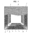
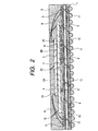
- Fig. 1 is a plan view showing an upper surface of a semiconductor device according to a first embodiment of the present invention
- Fig. 1 is a sectional view of the semiconductor device
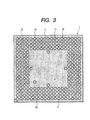
- Fig. 3 is a plan view showing a lower surface of the semiconductor device.
- the semiconductor device of this embodiment is a multi-chip module (MCM) wherein three chips 2A, 2B and 2C are mounted on a main surface of a package substrate 1 and are sealed with a molding resin 3.
- MCM multi-chip module
- three chips 2A, 2B and 2C are mounted on a main surface of a package substrate 1 and are sealed with a molding resin 3.
- two chips 2A and 2B are arranged side by side on the main surface of package substrate 1 and are electrically connected to wiring lines 5 on the package substrate 1 through plural Au bumps 4 formed on main surfaces of the chips 2A, 2B. That is, the chips 2A and 2B are each mounted in accordance with a flip-chip method.
- a gap is formed between the main surfaces (lower surfaces) of the chips 2A, 2B and the main surface of the package substrate 1, and an under-fill resin (sealing resin) 6 is injected into the said gap.
- the chip 2A is, for example, a silicon chip on which is formed a DRAM including a memory circuit having plural memory elements.
- the chip 2B is, for example, a silicon chip with a flash memory formed thereon.
- the chip 2C is disposed so as to straddle the two chips 2A and 2B and is bonded to upper surfaces of the chips 2A and 2B with an adhesive 7. Bonding pads 13 formed on a main surface of the chip 2C are electrically connected to bonding pads 9 on the package substrate 1 through plural Au wires 8. That is, the chip 2C is mounted in accordance with a wire bonding method.
- the chip 2C is, for example, a silicon chip formed with a high-speed microprocessor (MPU: ultra-small sized processor) including a processor circuit which operates in accordance with programs.
- MPU ultra-small sized processor
- the package substrate 1 on which the three chips 2A, 2B and 2C are mounted is a multi-layer wiring substrate constituted mainly by a general-purpose resin such as an epoxy resin (glass fabric-based epoxy resin) which contains glass fiber.
- a general-purpose resin such as an epoxy resin (glass fabric-based epoxy resin) which contains glass fiber.
- Four to six layers of wiring lines 5 are formed on its main surface (upper surface), lower surface, and also in the interior thereof.
- solder bumps 11 which constitute external connecting terminals of the multi-chip module (MCM) are connected to the electrode pads 10 respectively.
- the multi-chip module (MCM) is mounted for example on a wiring substrate of an electronic device through the solder bumps 11.
- the main surface and the lower surface of the package substrate 1 are coated with a solder resist (insulating film) 12 such as an epoxy resin or an acrylic resin, exclusive of the surfaces of connections between the wiring lines 5 and the chips 2A, 2B, bonding pads 9 and electrode pads 10.
- a dimensional example of the multi-chip module (MCM) will now be described.
- External dimensions of the package substrate 1 are 13 mm long by 13 mm wide and 0.3 mm thick.
- the thickness of each of the chips 2A, 2B, and 2C mounted on the package substrate 1 is 0.15 mm.
- the spacing between two chips 2A and 2B which are arranged side by side is 20 to 100 ⁇ m.
- the thickness of the molding resin 3 which seals the chips 2A, 2B, and 2C is 0.66 mm, and the distance from an upper surface of the molding resin 3 to a lower end of each solder bump 11, i.e., the mounting height of the multi-chip module (MCM) is 1.468 mm.
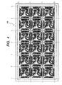
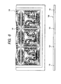
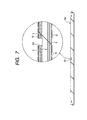
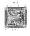
- Figs. 4 to 8 illustrate a rectangular substrate (hereinafter referred to as "multi-wiring substrate 100") used in manufacturing the multi-chip module (MCM), of which Fig. 4 is an entire plan view showing a main surface (chip mounting surface) of the multi-wiring substrate 100, Fig. 5 is an entire plan view showing a back side of the multi-wiring substrate 100, Fig. 6 comprises a plan view and a side view, showing a part of the multi-wiring substrate 100, Fig. 7 is a sectional view showing a part of the multi-wiring substrate 100, and Fig. 8 is an enlarged plan view showing a part (an area corresponding to one package substrate) of the multi-wiring substrate 100.
- the multi-wiring substrate 100 is a substrate serving as a matrix of the package substrate 1 described previously. By dicing the multi-wiring substrate 100 in a lattice shape along dicing lines L shown in Figs. 4 and 5 into individual pieces there are obtained plural package substrates 1.
- the multi-wiring substrate 100 is a multi-layer wiring substrate constituted mainly by a general-purpose resin such as a glass fabric-based epoxy resin. On the main surface of the multi-wiring substrate 100 are formed wiring lines 5 and bonding pads 9, while on a back side thereof are formed electrode pads 10. Further, in the interior of the multi-wiring substrate 100 are formed plural layers of wiring lines 5.
- MCM multi-chip module
- the wiring lines 5 and the bonding pads 9 on the main surface of the multi-wiring substrate 100, as well as the electrode pads 10 on the back side thereof, are formed by etching Cu foil affixed to both sides of the multi-wiring substrate 100.
- the surfaces of regions not covered with solder resist 12, i.e., the surfaces of regions to which Au bumps 4 of chips 2A and 2B are connected are plated with Ni and Au.
- the surfaces of the bonding pads 9 and electrode pads 10 are also plated with Ni and Au.
- platings can be done by an electroless plating method, but the plating layer formed by the electroless plating method is thin and it is difficult to ensure a sufficient bonding strength when Au wires 4 are connected onto the bonding pads 9. For this reason, the above Ni and Au platings are performed by an electrolytic plating method which can afford a thicker film than in the electroless plating method.
- the plating is carried out in a state in which the wiring lines 5, bonding pads 9 and electrode pads 10 are conducting in the whole area of the multi-wiring substrate 100, then the wiring lines 5 lying on the dicing lines L are cut with a router, and thereafter each package substrate-forming area is tested for continuity. Therefore, as shown in Figs. 6 and 7, grooves 101 formed by cutting the wiring lines 5 in the above-mentioned areas with the router are left over along the dicing lines L on the main surface of the multi-wiring substrate 100.
- the continuity test can be conducted in an individual manner. Besides, since the multi-wiring substrate 100 is not cut off completely, it is possible to facilitate a block molding process and the substrate conveyance which follows. End portions of cut wiring lines are exposed from side faces of the grooves 101.
- plural bonding pads 13 are formed in the peripheral portion of each package substrate-forming area so as to surround the chip mounting area.
- the bonding pads 13 are arranged in two rows along the four sides of the package substrate-forming area.
- a dam area 16 is formed between the bonding pads 13 and the chip mounting area.
- the dam area 16 is an area in which the solder resist 12 is not formed, and its surface height is lower than the areas located inside and outside the dam area and in which the solder resist 12 is formed.
- the dam area 16 functions to prevent the under-fill resin 6 from flowing to the peripheral portion of the package substrate-forming area, i.e., to the area where the bonding pads 13 are formed.
- a resin tape 6a is affixed to the main surface of the multi-wiring substrate 100.
- the resin tape 6a is formed of a thermosetting epoxy resin with silica dispersed therein, the silica having a particle diameter of about 3 ⁇ m.
- the resin tape 6a is cut beforehand into a size almost equal to two chips (2A, 2B).
- the resin tape 6a may also be constituted, for example, by an anisotropic conductive resin (ACF) with a fine conductive powder dispersed therein.
- ACF anisotropic conductive resin
- the multi-wiring substrate 100 which is left standing in the atmosphere, so if the resin tape 6a is affixed to the main surface of the multi-wiring substrate 100 as it is, the adhesion between the two may be deteriorated. Therefore, when the resin tape 6a is to be affixed to the substrate main surface, it is desirable that the multi-wiring substrate 100 be baked just before the affixing to remove moisture. For example, baking conditions involve a temperature of 125°C and a baking time of 2 hours or so. If the multi-wiring substrate 100 is treated with plasma after the baking process to activate the surface of the substrate, it is possible to further improve the adhesion between the resin tape 6a and the multi-wiring substrate 100.
- two chips 2A and 2B are mounted onto the resin tape 6a affixed to the main surface of the multi-wiring substrate 100.
- the gap between the chips 2A and 2B is set at a value of 20 to 100 ⁇ m.
- the particle diameter of silica contained in the resin tape 6a is about 3 ⁇ m, so even if the gap between the two chips is made as narrow as 20 ⁇ m, it is possible to inject the under-fill resin 6 into the above-mentioned gap.
- the gap between the chips 2A and 2B is too wide, the gap is not filled to a complete extent with the under-fill resin 6 and an air pocket (void) may occur in the gap in a later molding process. Further, widening the chip-to-chip gap means enlarging the area of each wiring substrate and thus impedes high-density packaging.
- Au bumps 4 are formed beforehand on the main surface of the chip 2A with a DRAM formed thereon. Also on the main surface of the chip 2B with a flash memory formed thereon there are formed Au bumps 4 beforehand in the same manner, as shown in Fig. 14. These Au bumps 4 are formed in the final step of a wafer process. More specifically, after completion of the ordinary wafer process, Au bumps 4 are formed on bonding pads of wafer in accordance with a ball bonding method and thereafter the wafer is diced to obtain individual chips 2A and 2B.
- bonding pads of a DRAM are arranged in one row centrally of a chip, but bonding pads of a flash memory are arranged in two rows along short sides of a chip. Therefore, the bonding pads of the DRAM are narrower in pad pitch than the bonding pads of the flash memory, with consequent reduction also in pad diameter, (for example, in case of the terminal pitch of the flash memory being 150 ⁇ m, that of the DRAM is about 85 ⁇ m).
- Au wires of a small diameter are used when forming Au bumps 4 on the bonding pads of the DRAM, while Au wires of a large diameter (e.g., 30 ⁇ m dia.) are used when forming Au bumps 4 on the bonding pads of the flash memory.
- Au wires used in forming Au bumps 4 on the bonding pads of the flash memory are the same in diameter (e.g., 20 ⁇ m dia.) as the Au wires used in forming Au bumps 4 on the bonding pads of the DRAM.
- the Au bumps 4 formed by using fine Au wires are reduced in the area of contact thereof with the bonding pads and thus there may occur a state of poor contact.
- a multi-stage bump structure wherein Au bumps 4 are superimposed and bonded onto Au bumps 4.
- a heat tool (also called heat block) 102 having a flat bottom is pushed onto the two chips 2A and 2B.
- the pushing pressure of the heat tool 102 is 15 kg/10 mm 2 and the heating temperature is 235°C, whereby not only the resin tape 6a melts and the gap between the chips 2A, 2B and the multi-wiring substrate 100 and the gap between the chips 2A and 2B are filled with the under-fill resin 6, but also the Au bumps 4 on the chips 2A, 2B and the wiring lines (not shown in Fig. 15) on the multi-wiring substrate 100 are connected together electrically.
- the under-fill resin 6 is formed for protecting the main surfaces (the surfaces on which semiconductor elements and electrodes (bonding pads) are formed) of the chips 2A and 2B, for bonding the chips 2A and 2B to the multi-wiring substrate 100, and for ensuring a required strength of connection between the bump electrodes 4 and the electrode pads on the multi-wiring substrate 100.
- the gap between the chips 2A, 2B and the multi-wiring substrate 100 and the gap between the chips 2A and 2B are filled with the under-fill resin 6.
- this method for example in comparison with a resin filling method wherein a liquid under-fill resin is fed around the chips 2A and 2B with use of a dispenser, it is possible to diminish the amount of the under-fill resin 6 protruded to around the chips 2A and 2B and therefore the bonding pads 9 on the multi-wiring substrate 100, which are arranged so as to surround the chips 2A and 2B, are not covered with the under-fill resin 6.
- a chip 2C is mounted on the two chips 2A and 2B.
- bonding pads 13 are formed along the four sides of a main surface of the chip 2C on which is formed a microprocessor.
- the number of the bonding pads 13 is larger than that of the bonding pads formed on the chips 2A and 2B.
- the chip with a relatively small number of bonding pads is mounted by a face-down method, while the chip with a relatively large number of bonding pads is mounted by a face-up method, whereby the wiring density (wiring pitch) of the wiring substrate and the distribution of wiring are decreased and it is possible to provide a high-density package of low cost.
- the chip 2C is disposed centrally of each package substrate-forming area so that the Au wires 8 which connect the multi-wiring substrate 100 and the chip 2C become as uniform as possible in length.
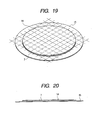
- a tape-like adhesive 7 pre-cut to the same size as the chip 2C is affixed to a back side of the chip 2C in the following manner. As shown in Figs. 19 and 20, at the time of affixing a dicing tape 15 to a back side of a wafer 14 after completion of the ordinary wafer process, the tape-like adhesive 7 is sandwiched in between the wafer 14 and the dicing tape 15 and in this state the wafer 14 is diced to obtain the chip 2C.
- the dicing tape 15 is removed from the back side of the chip 2C, whereby the adhesive 7 of the same size as the chip 2C is left unremoved on the back side of the chip 2C.
- the adhesive 7 there is used a polyimide resin-based adhesive for example.
- the multi-wiring substrate 100 is heated within a heating furnace at 180°C for 1 hour or so, whereby the adhesive 7 softens and the chip 2C is bonded onto the chips 2A and 2B.
- the bonding pads 9 on the multi-wiring substrate 100 and the bonding pads 13 (not shown in Figs. 21 and 22) on the chip 2C are connected together through Au wires 8.
- the connection of the Au wires 8 is performed by means of a wire bonder which uses both ultrasonic oscillation and thermocompression bonding.
- the multi-wiring substrate 100 is loaded into a molding die (not shown) and the whole of the main surface of the multi-wiring substrate 100 is sealed with molding resin 3 at a time.
- the molding resin is a thermosetting epoxy resin with silica dispersed therein, the silica having a particle diameter of about 70 to 100 ⁇ m for example.
- the gap between the chips 2A, 2B and the multi-wiring substrate 100 and the gap between the chips 2A and 2B are filled with the under-fill resin 6 in advance, there is no fear of an air pocket (void) being formed in those gaps when the main surface of the multi-wiring substrate 100 is resin-sealed.
- solder bumps 11 are connected to the electrode pads 9 (not shown in Fig. 25) formed on the back side of the multi-wiring substrate 100.
- the connection of the solder bumps 11 is performed, for example, by feeding solder balls of a low melting Pb-Sn eutectic alloy to the surfaces of the electrode pads 9 and by subsequently reflowing the solder balls.
- the multi-wiring substrate 100 is diced into individual pieces along the dicing lines L shown in Figs. 4 and 5, whereby the multi-chip module (MCM) of this embodiment shown in Figs. 1 to 3 is completed.
- MCM multi-chip module
- a dicing blade having a width smaller than the width of each of the grooves 101 (see Figs. 6 and 7) formed in the dicing lines L of the multi-wiring substrate 100.
- the multi-chip module (MCM) resulting from the dicing process is mounted through the solder bumps 11 onto a mounting substrate, e.g., a printed circuit board (PCB).
- a mounting substrate e.g., a printed circuit board (PCB).
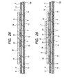
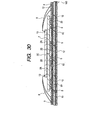
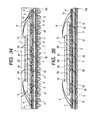
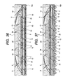
- a method of manufacturing a semiconductor device according to a second embodiment of the present invention will be described below step by step with reference to Figs. 27 to 34.
- Au bumps 4 are formed on the main surface of the chip 2A with a DRAM formed thereon and also on the main surface of the chip 2B with a flash memory formed thereon, but in this second embodiment there are used solder bumps 20 instead of Au bumps 4.
- Fig. 27 is a plan view showing a state in which solder bumps 20 are formed on a main surface of a chip 2A with a DRAM formed thereon. As shown in the same figure, the solder bumps 20 are arranged in the form of an array on the main surface of the chip 2A. Bonding pads 13 and the solder bumps 20 are electrically connected with each other through Cu wiring lines 21 called re-wiring lines.
- the Cu wiring lines 21 function as an interposer for converting the pitch of the bonding pads 13 to the pitch of the solder bumps 20, whereby the pitch of the solder bumps 20 can be made wider than that of the bonding pads 13, so that the expensive build-up substrate need not be used as the package substrate 1 and it is possible to use a less expensive resin substrate having a wide pitch of wiring lines 5.
- the Cu wiring lines 21 and the solder bumps 20 are formed in the final step of the wafer process. That is, after an organic insulating film such as a polyimide resin film is formed on a surface protecting film of a wafer, Cu wiring lines 21 are formed on the organic insulating film by an electrolytic plating method for example. The Cu wiring lines 21 and the bonding pads 13 are electrically connected with each other through through-holes formed in the organic insulating film on the bonding pads 13.
- the solder bumps 20 are formed by printing solder paste to one ends of the Cu wiring lines 21 by a screen printing method and by subsequently heating the wafer to melt the solder paste.
- solder bumps 20 are constituted by a Pb-Sn alloy (liquidus line temperature: 320°C to 325°C) including 2 wt% of Sn.
- Cu wiring lines 21 and solder bumps 20 are formed in the same manner also on a main surface of a chip 2B with a flash memory formed thereon.
- the chips 2A and 2B are positioned in each of package substrate-forming areas of a multi-wiring substrate 100, then the multi-wiring substrate 100 is heated to about 340°C within an electric furnace to reflow the solder bumps 20, thereby electrically connecting the solder bumps 20 on the chips 2A and 2B with the wiring lines 5 on the multi-wiring substrate 100.
- a chip 2C is mounted on the two chips 2A and 2B.
- bonding of the chip 2C with the chips 2A and 2B is performed using an adhesive 7 affixed to a back side of the chip 2C.
- connection of the Au wires 8 is performed for example by means of a wire bonder which uses both ultrasonic oscillation and thermocompression bonding.
- a liquid under-fill resin 6 is fed to the peripheral portions of the chips 2A and 2B with used of a dispenser or the like and is thereafter heated and cured, whereby the gap between the chips 2A, 2B and the multi-wiring substrate 100 and the gap between the chips 2A and 2B are filled with the under-fill resin 6. Since the liquid under-fill resin 6 is high in fluidity and the particle diameter (about 3 ⁇ m) of the silica filler added therein is smaller than the gap (about 20 to 100 ⁇ m) between the chips 2A and 2B, the chip-to-chip gap can be filled completely with the under-fill resin 6.
- the liquid under-fill resin 6 when the liquid under-fill resin 6 is fed to the peripheral portions of the chips 2A and 2B, it is also fed to the peripheral portions of the package substrate-forming areas to cover the surfaces of the bonding pads 13 with the under-fill resin 6. It is not necessary for the under-fill resin 6 to cover the surfaces of all the bonding pads 13 completely. If the under-fill resin 6 is cured in this state, one end portions of the Au wires 8 connected to the surfaces of the bonding pads 13 are fixed by the under-fill resin 6, so that the reliability of connection between the bonding pads 13 and the Au wires 8 is improved. Besides, since the wire bonding process is completed before the injection of the under-fill resin 6, it is possible, with the under-fill resin 6, to avoid contamination of the electrode pads formed on the substrate.
- the multi-wiring substrate 100 is loaded into a molding die (not shown) and the whole of a main surface thereof is sealed with a molding resin 3 at a time.
- the molding resin 3 is, for example, a thermosetting epoxy resin with silica dispersed therein, the silica having a particle diameter of about 70 to 100 ⁇ m.
- the gap between the chips 2A, 2B and the multi-wiring substrate 100 and the gap between the chips 2A and 2B are filled with the under-fill resin 6 beforehand, there is no fear of an air pocket (void) being formed when the main surface of the multi-wiring substrate 100 is resin-sealed.
- the solder bumps 11 are connected to electrode pads 10 formed on a back side of the multi-wiring substrate 100.
- the multi-chip module (MCM) of this embodiment is completed by dicing the multi-wiring substrate 100 in the same manner as in the first embodiment.
- solder bumps 20 on chips 2A, 2B and wiring lines 5 on a multi-wiring substrate 100 are electrically connected with each other, then a chip 2C is mounted on the two chips 2A and 2B through an adhesive 7, and thereafter bonding pads 9 on the multi-wiring substrate 100 and bonding pads 13 on the chip 2C are connected together through Au wires 8.
- the multi-wiring substrate 100 is loaded into a molding die (not shown) and the whole of a main surface thereof is sealed with resin at a time.
- a molding resin 3 with a silica filler added therein the silica filler having a particle diameter of about 3 ⁇ m, as is the case with the under-fill resin 6 used in the previous first and second embodiments.
- the particle diameter of the silica filler added to the molding resin 3 is smaller than the gap (about 20 to 100 ⁇ m) between the chips 2A and 2B, so that the gap between the chips 2A, 2B and the multi-wiring substrate 100, as well as the gap between the chips 2A and 2B, can be filled with the molding resin 3 completely.
- This molding resin 3 is expensive in comparison with the molding resin 3 with silica of about 70 to 100 ⁇ m in particle diameter added therein which was used in the first and second embodiments, but permits omission of the step of injecting the under-fill resin 6 into the gap between the chips 2A, 2B and the multi-wiring substrate 100 and the gap between the chips 2A and 2B.
- solder bumps 11 are connected to electrode pads 9 on a back side of the multi-wiring substrate 100 in the same way as in the first and second embodiments. Thereafter, though not shown, the multi-wiring substrate 100 is diced in the same manner as in the first and second embodiment to complete the multi-chip module (MCM) of this embodiment.
- MCM multi-chip module
- Fig. 38 is a sectional view showing a semiconductor device according to a fourth embodiment of the present invention and Fig. 39 is a sectional view showing a part of Fig. 38 on a larger scale.
- MCM multi-chip module
- a chip 2A with a DRAM formed thereon is mounted on a main surface of a package 1
- a chip 2C with a high-speed microprocessor (MPU) formed thereon is stacked on the chip 2A, and the two chips 2A and 2C are sealed with a molding resin 3.
- MPU microprocessor
- the underlying chip 2A is electrically connected to wiring lines 5 on the package substrate 1 through Au bumps 4 formed on the main surface of the package substrate 1. That is, the chip 2A is mounted in accordance with a flip-chip method. A gap is formed between a main surface (lower surface) of the chip 2A and the main surface of the package substrate 1 and is filled with an under-fill resin 6.
- the overlying chip 2C is bonded to an upper surface of the chip 2A through an adhesive 7. Bonding pads 13 formed on a main surface of the chip 2C are electrically connected to bonding pads 9 on the package substrate 1 through plural Au wires 8. That is, the chip 2C is mounted in accordance with a wire bonding method.
- Plural electrode pads 10 connected electrically to the wiring lines 5 are arranged in the form of an array on a lower surface of the package substrate 1 which packages the two chips 2A and 2C, and solder bumps 11 which constitute external connecting terminals (pins) of the multi-chip module (MCM) are connected respectively to the electrode pads 10.
- the main surface and lower surface of the package substrate 1 are coated with a solder resist 12 such as an epoxy resin or an acrylic resin exclusive of the surfaces of the connections between the wiring lines 5 and the chip 2A and of the bonding pads 9 and electrode pads 10.
- the chip 2A with a DRAM formed thereon has a rectangular shape in plan and plural Au bumps 4 are arranged in a row centrally of the main surface of the chip 2A.
- the chip 2C with a microprocessor formed thereon has a generally square shape in plan and bonding pads 13 are formed along the four sides of the main surface of the chip 2C.
- the number of bonding pads 13 formed on the chip 2C is larger than the number of bonding pads (Au bumps 4) formed on the chip 2A.
- the chip 2A having a small number of bonding pads and a large minimum pitch of bonding pads and the chip 2C having a large number of bonding pads and a small minimum pitch of bonding pads are to be stacked one on the other, the chip 2A having a large minimum pitch of bonding pads is face-down mounted through Au bumps 4, while the chip 2C having a small minimum pitch of bonding pads is face-up mounted by wire bonding.
- the requirement for the wiring density of the package substrate 1 can be eased, so that it becomes possible to use a less expensive substrate as the package substrate 1 and provide a package of a low cost and which permits a high-density packaging.
- the overhanging quantity of the under-fill resin 6 from the underlying chip 2A to the outer periphery thereof is controlled by controlling the amount of the same resin fed, it is difficult to control the overhanging quantity accurately.
- the bonding pads on the main surface of the package substrate 1 are contaminated by excess overhanging of the under-fill resin 6, there is a fear that a disconnection defect between the bonding wires and the bonding pads 9 may occur in the subsequent wire bonding step.
- the length (h) of an unsupported portion of the overlying chip 2C is set at a value of not larger than 1.5 mm, preferably not larger than 1 mm.
- Fig. 40 is a layout diagram of pins (terminals) of the multi-chip module (MCM) according to this embodiment.
- the package substrate 1 used in the multi-chip module (MCM) of this embodiment has a pin layout common to a package substrate designed for mounting a single chip 2C with a high-speed microprocessor formed thereon. Therefore, out of the pins shown in Fig. 40, control pins (CASL, RASL, CS3, RDWR, WE1, WE0, all of which will hereinafter be referred to as "C"), address pins (A0 to A14, all "A” hereinafter), and data pins (D0 to D15, all “D” hereinafter), are connected using common wiring lines 5.
- control pins (CASL, RASL, CS3, RDWR, WE1, WE0, all of which will hereinafter be referred to as "C")
- address pins A0 to A14, all "A” hereinafter
- data pins D0 to D15, all "D” hereinafter
- test pins 11t for the chip 2A are arranged just under the chip mounting area.
- the test pins 11t are arranged near the center of the package substrate 1, the wiring lines 5 connected to the test pins become longer and hence the wiring design for the package substrate 1 becomes difficult.
- the test pins 11t are arranged in adjacency to the area where other pins (solder bumps 11) are arranged, the distance between the other pins (solder bumps 11) and the test pins 11t becomes shorter, so that it becomes difficult to make layout of the wiring lines 5 connected to other pins which are adjacent to the test pins 11t; in this case, it becomes difficult to make wiring design for the mounting substrate which is for mounting the MCM.
- the test pins 11t should not be arranged in adjacency to the area where other pins (solder bumps 11) are arranged, but it is preferable that the test pins 11t be arranged inside the other pins through a spacing of one row. In the case where two or more non-connection pins are included in the other pins (solder bumps 11), the test pins 11t may be arranged in the area where the non-connection pins are arranged.
- the multi-chip module is constituted using the package substrate 1 having a pin layout (exclusive of the test pins 11t) common to the package substrate which is designed for mounting a single chip 1C with a high-speed microprocessor (MPU) formed thereon.
- MPU microprocessor
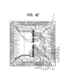
- Fig. 42 illustrates a layout of a group of address pins (A) and a group of data pins (D) on the package substrate 1.
- the package substrate 1 for packaging the chip 2C having a large number of pins like a high-speed microprocessor (MPU)
- MPU microprocessor
- address pins (A) are concentrated in a specific area and so are data pins (D)
- the group of address pins (A) and the group of data pins (D) are arranged adjacent each other, whereby it is possible to shorten the wiring length for example when the package substrate 1 is connected to an external memory chip.
- a group of address pins (A) is disposed on one end side and a group of data pins (D) is disposed on an opposite end side in the longitudinal direction of the chip 2A, as shown in Fig. 43.
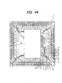
- the chip 2A in case of constituting the multi-chip module (MCM) by stacking the chip 2C on the chip 2A as in this embodiment, it is preferable for the chip 2A to be oriented so that a group of address pins (A) on the package substrate 1 and a group of address pins (A) on the chip 2A are arranged adjacent each other and so are a group of data pins (D) on the package substrate 1 and a group of data pins (D) on the chip 2A, as shown in Fig. 44.
- a group of wiring lines 5 for connection between the group of address pins (A) on the package substrate 1 and the group of address pins on the chip 2A and a group of wiring lines 5 for connection between the group of data pins (D) on the package substrate 1 and the group of data pins (D) on the chip 2A can be prevented from crossing each other and therefore the wiring design of the package substrate 1 becomes easier.
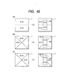
- Figs. 45(a) to (c) show a layout example of a group of address pins (A) and a group of data pins (D) on the package substrate 1, in which the area indicated with symbol (D>A) represents an area in which data pins (D) are mainly arranged, while the area indicated with symbol (A>D) represents an area in which address pins (A) are mainly arranged.
- a group of wiring lines 5 for connection between a group of address pins (A) on the package substrate 1 and a group of address pins (A) on the chip 2A and a group of wiring lines 5 for connection between a group of data pins (D) on the package substrate 1 and a group of data pins (D) on the chip 2A can be prevented from crossing each other on the package substrate 1.
- the chip 2C is stacked on the chip 2A with a DRAM formed thereon, but also in case of constituting a multi-chip module (MCM) by stacking the chip 2C on the chip 2B with a flash memory formed thereon, as shown in Fig. 14 for example, it is preferable that the chip 2B be oriented in the same manner as above.
- a group of address pins (A) is disposed along one of two short sides opposed to each other and a group of data pin (D) is disposed along the other short side.
- the chip 2B is oriented so that a group of address pins (A) on the package substrate 1 and a group of address pins (A) on the chip 2B are arranged adjacent each other and so are a group of data pins (D) on the package substrate 1 and a group of data pins (D)O on the chip 2B, whereby a group of wiring lines 5 for connection between the group of address pins (A) on the package substrate 1 and a group of address pins (A) on the chip 2B and a group of wiring lines 5 for connection between the group of data pins (D) on the package substrate 1 and the group of data pins (D) on the chip 2B can be prevented from crossing each other on the package substrate 1.
- the number of bonding pads 9 on the module substrate 1 necessary for the connection thereof with the MPU chip 2C is very large, so by arranging the bonding pads 9 along the outer periphery of the module substrate 1, it is possible to ensure a required spacing of the bonding pads 9.
- a multi-chip module MCM
- MCM multi-chip module
- a single chip 2A with DRAM formed thereon and a dummy chip 2D are arranged side by side on the main surface of the package substrate 1 and the chip 2C is stacked on the two chips 2A and 2D.
- the dummy chip 2D is formed, for example, by dicing a mirror polish wafer not formed with an integrated circuit and by equalizing its thickness to the sum of the thickness of chip 2A and the height of Au bumps 4.
- Such a mounting method is effective for example in the case where an outside diameter of the overlying chip 2C is much larger than that of the underlying chip 2A and the overhanging quantity (h) of the overlying chip 2C relative to the underlying chip 2A described in connection with Fig. 39 cannot be set at a value of 1.5 mm or less.
- the chip mounted on the package substrate by the flip-chip method is not limited to DRAM alone, flash memory alone, or a combination of DRAM and flash memory.
- Various memory chips may be combined arbitrarily such as DRAMs with each other, flash memories with each other, or a combination of DRAM or flash memory with SRAM (Static Random Access Memory).
- SRAM Static Random Access Memory
- the chip to be stacked on the memory chips no limitation is made to a microprocessor or ASIC, but there may be used a chip formed with LSI of a narrower pitch than memory chips. Further, the number of chips mounted on the package substrate is not limited to two or three.
- the package substrate there may be mounted other small-sized electronic parts than chips, such as capacitors and resistors.
- other small-sized electronic parts such as capacitors and resistors.
- capacitors and resistors For example, by mounting a chip capacitor along the outer periphery of a memory chip, it is possible to diminish noise produced during operation of the memory chip and thereby attain a high-speed operation.
Landscapes
- Encapsulation Of And Coatings For Semiconductor Or Solid State Devices (AREA)
- Wire Bonding (AREA)
- Physics & Mathematics (AREA)
- Geometry (AREA)
- Internal Circuitry In Semiconductor Integrated Circuit Devices (AREA)
Abstract
Of three chips (2A), (2B), and (2C) mounted on a main
surface of a package substrate (1) in a multi-chip module
(MCM), a chip (2A) with a DRAM formed thereon and a chip
(2B) with a flash memory formed thereon are electrically
connected to wiring lines (5) of the package substrate (1)
through Au bumps (4), and a gap formed between main
surfaces (lower surfaces) of the chips (2A), (2B) and a
main surface of the package substrate (1) is filled with an
under-fill resin (6). A chip (2C) with a high-speed
microprocessor formed thereon is mounted over the two chips
(2A) and (2B) and is electrically connected to bonding pads
(9) of the package substrate (1) through Au wires (8).
Description
The present invention relates to a semiconductor
device and a method of manufacturing the same.
Particularly, the present invention is concerned with a
technique applicable effectively to a multi-chip module
(MCM) or a mutli-chip package (MCP) wherein plural
semiconductor chips are mounted on one and same wiring
substrate.
As a measure for increasing the capacity of such
memory LSIs as flash memory and DRAM (Dynamic Random Access
Memory) there have been proposed various memory module
structures wherein semiconductor chips (memory chips) with
such memory LSIs stacked thereon are sealed in a single
package.
For example, Japanese Unexamined Patent Publication
No. Hei 4(1992)-302164 discloses a package structure
wherein plural semiconductor chips having the same function
and the same size are stacked in the shape of stairs
through insulating layers, and bonding pads exposed to the
stair portion of each semiconductor chip are electrically
connected to inner leads of a package through wires.
In Japanese Unexamined Patent Publication No. Hei
11(1999)-204720 there is disclosed a package structure
wherein a first semiconductor chip is mounted on an
insulating substrate through a thermocompression-bonded
sheet, a second semiconductor chip smaller in external size
than the first semiconductor chip is mounted on the first
semiconductor chip through a thermocompression-bonded sheet,
bonding pads on the first and second semiconductor chips
and a wiring layer on the insulating substrate are
electrically connected with each other through wires, and
the first and second semiconductor chips and the wires are
sealed with resin.
The inventors in the present case are developing a
multi-chip module wherein plural semiconductor chips
(hereinafter referred to simply as "chips") are mounted
within a single package.
According to the multi-chip module under development
by the present inventors, a chip having a DRAM (Dynamic
Random Access Memory), a chip having a flash memory, and a
chip having a high-speed microprocessor (MPU: ultra-small
sized processor), are sealed within a single resin package,
with the intention of realizing a more versatile system
than a conventional memory module having plural memory
chips sealed with resin.
In the multi-chip module in question, in order to
diminish the mounting area, out of the three chips, the
chip having a DRAM and the chip having a flash memory are
arranged side by side on a main surface of a package
substrate and are packaged in accordance with a flip-chip
method, while the third chip having a microprocessor is
stacked on the above two memory chips and is packaged in
accordance with a wire bonding method.
In the multi-chip module of the above structure,
however, when viewed from the standpoint of high-density
packaging, the spacing between the two memory chips
arranged side by side is several µm or so and is thus very
narrow; besides, the third chip is stacked on those two
memory chips, so if an attempt is made to seal these memory
chips with a molding resin, there arises the problem that
the molding resin is difficult to enter the gap between the
two memory chips.
Generally, a silica filler is mixed into the molding
resin in order to let the thermal expansion coefficient of
the molding resin approximate that of a silicon chip.
However, the particle diameter (e.g., 70 to 100 µm) of the
silica filler is larger than the spacing (several ten µm)
between the two memory chips referred to above, so this is
one reason why the molding resin is difficult to be
injected into the chip-to-chip gap.
If the gap between the two memory chips is not filled
with the molding resin, an air pocket (void) is formed
therein. Since thermal expansion of the air present in the
void is repeated, the molding resin and the chips are
peeled off from each other to a greater extent with the
void as the center. As a result, for example when an MCP
is mounted on a mounting substrate with use of a solder
reflow technique, there is a fear that a package crack may
occur.
It is an object of the present invention to provide a
technique for improving the reliability and attaining high-density
packaging and low cost of a multi-chip module
wherein plural chips are mounted on a wiring substrate and
a main surface thereof is sealed with resin.
It is another object of the present invention to
provide a technique for improving the reliability of a
multi-chip module wherein on plural chips there is stacked
another chip and these chips are sealed with resin.
It is a further object of the present invention to
provide a technique capable of reducing the manufacturing
cost of a multi-chip module wherein on plural chips there
is stacked another chip and these chips are sealed with
resin.
The above and other objects and novel features of the
present invention will become apparent from the following
description and the accompanying drawings.
Typical modes of the invention disclosed herein will
be described below briefly.
A multi-chip module according to the present
invention comprises a wiring substrate with plural wiring
lines and plural electrode pads formed on a main surface
thereof, a first semiconductor chip mounted in a first area
of the main surface of the wiring substrate and connected
electrically to the wiring lines through a plurality of
first bump electrodes, a second semiconductor chip mounted
in a second area of the main surface of the wiring
substrate and connected electrically to the wiring lines
through a plurality of second bump electrodes, a third
semiconductor chip stacked on the first and second
semiconductor chips and connected electrically to the
electrode pads through a plurality of bonding wires, a
first sealing resin injected into a gap between the first,
second semiconductor chips and the wiring substrate and
also injected into a gap formed between the first and
second semiconductor chips, and a second sealing resin
which hermetically seals the first, second and third
semiconductor chips.
A multi-tip module manufacturing method according to
the present invention comprises the following steps:
Embodiments of the present invention will be
described in detail hereinunder with reference to the
accompanying drawings. In all of the drawings for
illustration of the embodiments, portions having the same
functions are identified by like reference numerals, and
repeated explanations thereof will be omitted.
Fig. 1 is a plan view showing an upper surface of a
semiconductor device according to a first embodiment of the
present invention, Fig. 1 is a sectional view of the
semiconductor device, and Fig. 3 is a plan view showing a
lower surface of the semiconductor device.
The semiconductor device of this embodiment is a
multi-chip module (MCM) wherein three chips 2A, 2B and 2C
are mounted on a main surface of a package substrate 1 and
are sealed with a molding resin 3. Of the three chips 2A
to 2C, two chips 2A and 2B are arranged side by side on the
main surface of package substrate 1 and are electrically
connected to wiring lines 5 on the package substrate 1
through plural Au bumps 4 formed on main surfaces of the
chips 2A, 2B. That is, the chips 2A and 2B are each
mounted in accordance with a flip-chip method.
A gap is formed between the main surfaces (lower
surfaces) of the chips 2A, 2B and the main surface of the
package substrate 1, and an under-fill resin (sealing
resin) 6 is injected into the said gap. The chip 2A is,
for example, a silicon chip on which is formed a DRAM
including a memory circuit having plural memory elements.
The chip 2B is, for example, a silicon chip with a flash
memory formed thereon.
The chip 2C is disposed so as to straddle the two
chips 2A and 2B and is bonded to upper surfaces of the
chips 2A and 2B with an adhesive 7. Bonding pads 13 formed
on a main surface of the chip 2C are electrically connected
to bonding pads 9 on the package substrate 1 through plural
Au wires 8. That is, the chip 2C is mounted in accordance
with a wire bonding method. The chip 2C is, for example, a
silicon chip formed with a high-speed microprocessor (MPU:
ultra-small sized processor) including a processor circuit
which operates in accordance with programs.
The package substrate 1 on which the three chips 2A,
2B and 2C are mounted is a multi-layer wiring substrate
constituted mainly by a general-purpose resin such as an
epoxy resin (glass fabric-based epoxy resin) which contains
glass fiber. Four to six layers of wiring lines 5 are
formed on its main surface (upper surface), lower surface,
and also in the interior thereof.
On the lower surface of the package substrate 1 are
arranged plural electrode pads 10 in an array form, the
electrode pads 10 being electrically connected to the
wiring lines 5. Solder bumps 11 which constitute external
connecting terminals of the multi-chip module (MCM) are
connected to the electrode pads 10 respectively. The
multi-chip module (MCM) is mounted for example on a wiring
substrate of an electronic device through the solder bumps
11. The main surface and the lower surface of the package
substrate 1 are coated with a solder resist (insulating
film) 12 such as an epoxy resin or an acrylic resin,
exclusive of the surfaces of connections between the wiring
lines 5 and the chips 2A, 2B, bonding pads 9 and electrode
pads 10.
A dimensional example of the multi-chip module (MCM)
will now be described. External dimensions of the package
substrate 1 are 13 mm long by 13 mm wide and 0.3 mm thick.
The thickness of each of the chips 2A, 2B, and 2C mounted
on the package substrate 1 is 0.15 mm. The spacing between
two chips 2A and 2B which are arranged side by side is 20
to 100 µm. The thickness of the molding resin 3 which
seals the chips 2A, 2B, and 2C is 0.66 mm, and the distance
from an upper surface of the molding resin 3 to a lower end
of each solder bump 11, i.e., the mounting height of the
multi-chip module (MCM) is 1.468 mm.
Next, a method of manufacturing the semiconductor
device of this embodiment constructed as above will be
described below step by step with reference to Figs. 4 to
26.
Figs. 4 to 8 illustrate a rectangular substrate
(hereinafter referred to as "multi-wiring substrate 100")
used in manufacturing the multi-chip module (MCM), of which
Fig. 4 is an entire plan view showing a main surface (chip
mounting surface) of the multi-wiring substrate 100, Fig. 5
is an entire plan view showing a back side of the multi-wiring
substrate 100, Fig. 6 comprises a plan view and a
side view, showing a part of the multi-wiring substrate 100,
Fig. 7 is a sectional view showing a part of the multi-wiring
substrate 100, and Fig. 8 is an enlarged plan view
showing a part (an area corresponding to one package
substrate) of the multi-wiring substrate 100.
The multi-wiring substrate 100 is a substrate serving
as a matrix of the package substrate 1 described previously.
By dicing the multi-wiring substrate 100 in a lattice shape
along dicing lines L shown in Figs. 4 and 5 into individual
pieces there are obtained plural package substrates 1. The
illustrated multi-wiring substrate 100 is partitioned in
its long side direction into six blocks of package
substrate-forming areas and in its short side direction
into three blocks of package substrate-forming areas, so
that there are obtained 3 x 6 = 18 package substrates 1.
The multi-wiring substrate 100 is a multi-layer
wiring substrate constituted mainly by a general-purpose
resin such as a glass fabric-based epoxy resin. On the
main surface of the multi-wiring substrate 100 are formed
wiring lines 5 and bonding pads 9, while on a back side
thereof are formed electrode pads 10. Further, in the
interior of the multi-wiring substrate 100 are formed
plural layers of wiring lines 5. By fabricating the
package substrate 1 with use of an inexpensive general-purpose
resin it is possible to reduce the manufacturing
cost of the multi-chip module (MCM).
The wiring lines 5 and the bonding pads 9 on the main
surface of the multi-wiring substrate 100, as well as the
electrode pads 10 on the back side thereof, are formed by
etching Cu foil affixed to both sides of the multi-wiring
substrate 100. In the wiring lines 5 formed on the main
surface of the multi-wiring substrate 100, the surfaces of
regions not covered with solder resist 12, i.e., the
surfaces of regions to which Au bumps 4 of chips 2A and 2B
are connected, are plated with Ni and Au. The surfaces of
the bonding pads 9 and electrode pads 10 are also plated
with Ni and Au. These platings can be done by an
electroless plating method, but the plating layer formed by
the electroless plating method is thin and it is difficult
to ensure a sufficient bonding strength when Au wires 4 are
connected onto the bonding pads 9. For this reason, the
above Ni and Au platings are performed by an electrolytic
plating method which can afford a thicker film than in the
electroless plating method.
In the case where the surfaces of the wiring lines 5,
bonding pads 9 and electrode pads 10 are to be plated with
Ni and Au by the electrolytic plating method, the plating
is carried out in a state in which the wiring lines 5,
bonding pads 9 and electrode pads 10 are conducting in the
whole area of the multi-wiring substrate 100, then the
wiring lines 5 lying on the dicing lines L are cut with a
router, and thereafter each package substrate-forming area
is tested for continuity. Therefore, as shown in Figs. 6
and 7, grooves 101 formed by cutting the wiring lines 5 in
the above-mentioned areas with the router are left over
along the dicing lines L on the main surface of the multi-wiring
substrate 100. Since the wiring lines formed
continuously between package substrates for continuity test
are cut with the router, the continuity test can be
conducted in an individual manner. Besides, since the
multi-wiring substrate 100 is not cut off completely, it is
possible to facilitate a block molding process and the
substrate conveyance which follows. End portions of cut
wiring lines are exposed from side faces of the grooves 101.
As shown in Fig. 8, plural bonding pads 13 are formed
in the peripheral portion of each package substrate-forming
area so as to surround the chip mounting area. The bonding
pads 13 are arranged in two rows along the four sides of
the package substrate-forming area. Between the bonding
pads 13 and the chip mounting area is formed a dam area 16
so as to surround the chip mounting area. The dam area 16
is an area in which the solder resist 12 is not formed, and
its surface height is lower than the areas located inside
and outside the dam area and in which the solder resist 12
is formed. Thus, when injecting the under-fill resin 6
below the chips 2A and 2B, the dam area 16 functions to
prevent the under-fill resin 6 from flowing to the
peripheral portion of the package substrate-forming area,
i.e., to the area where the bonding pads 13 are formed.
For fabricating the multi-chip module (MCM) with use
of the multi-wiring substrate 100, as shown in Fig. 9 (a
sectional view showing an area corresponding to two package
substrates) and Fig. 10 (an enlarged plan view showing an
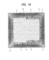
area corresponding to one package substrate), a resin tape
6a is affixed to the main surface of the multi-wiring
substrate 100. For example, the resin tape 6a is formed of
a thermosetting epoxy resin with silica dispersed therein,
the silica having a particle diameter of about 3 µm. The
resin tape 6a is cut beforehand into a size almost equal to
two chips (2A, 2B). The resin tape 6a may also be
constituted, for example, by an anisotropic conductive
resin (ACF) with a fine conductive powder dispersed therein.
As the resin tape 6a there may be used two sheets of tapes
divided into a size almost equal to the size of each
semiconductor chip 2A (2B).
Moisture contained in the atmosphere gets into the
multi-wiring substrate 100 which is left standing in the
atmosphere, so if the resin tape 6a is affixed to the main
surface of the multi-wiring substrate 100 as it is, the
adhesion between the two may be deteriorated. Therefore,
when the resin tape 6a is to be affixed to the substrate
main surface, it is desirable that the multi-wiring
substrate 100 be baked just before the affixing to remove
moisture. For example, baking conditions involve a
temperature of 125°C and a baking time of 2 hours or so.
If the multi-wiring substrate 100 is treated with plasma
after the baking process to activate the surface of the
substrate, it is possible to further improve the adhesion
between the resin tape 6a and the multi-wiring substrate
100.
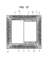
Next, by a face-down bonding method, as shown in Figs.
11 and 12, two chips 2A and 2B are mounted onto the resin
tape 6a affixed to the main surface of the multi-wiring
substrate 100. At this time, the gap between the chips 2A
and 2B is set at a value of 20 to 100 µm. The particle
diameter of silica contained in the resin tape 6a is about
3 µm, so even if the gap between the two chips is made as
narrow as 20 µm, it is possible to inject the under-fill
resin 6 into the above-mentioned gap. On the other hand,
if the gap between the chips 2A and 2B is too wide, the gap
is not filled to a complete extent with the under-fill
resin 6 and an air pocket (void) may occur in the gap in a
later molding process. Further, widening the chip-to-chip
gap means enlarging the area of each wiring substrate and
thus impedes high-density packaging.
As shown in Fig. 13, in accordance with a ball'
bonding method, Au bumps 4 are formed beforehand on the
main surface of the chip 2A with a DRAM formed thereon.
Also on the main surface of the chip 2B with a flash memory
formed thereon there are formed Au bumps 4 beforehand in
the same manner, as shown in Fig. 14. These Au bumps 4 are
formed in the final step of a wafer process. More
specifically, after completion of the ordinary wafer
process, Au bumps 4 are formed on bonding pads of wafer in
accordance with a ball bonding method and thereafter the
wafer is diced to obtain individual chips 2A and 2B.
Usually, bonding pads of a DRAM are arranged in one
row centrally of a chip, but bonding pads of a flash memory
are arranged in two rows along short sides of a chip.
Therefore, the bonding pads of the DRAM are narrower in pad
pitch than the bonding pads of the flash memory, with
consequent reduction also in pad diameter, (for example, in
case of the terminal pitch of the flash memory being 150 µm,
that of the DRAM is about 85 µm). Usually, therefore, Au
wires of a small diameter (e.g., 20 µm dia.) are used when
forming Au bumps 4 on the bonding pads of the DRAM, while
Au wires of a large diameter (e.g., 30 µm dia.) are used
when forming Au bumps 4 on the bonding pads of the flash
memory.
In the multi-chip module (MCM) of this embodiment,
however, since the third chip 2C is stacked on the two
chips 2A and 2B, it is necessary that the mounting height
of the chip 2A and that of the chip 2B be made equal by
making both chips equal in chip thickness and the diameter
of Au bumps 4. Therefore, in this embodiment, Au wires
used in forming Au bumps 4 on the bonding pads of the flash
memory are the same in diameter (e.g., 20 µm dia.) as the
Au wires used in forming Au bumps 4 on the bonding pads of
the DRAM. In this case, when the thickness (e.g., 25 µm)
of the solder resist 12 is taken into account, the Au bumps
4 formed by using fine Au wires are reduced in the area of
contact thereof with the bonding pads and thus there may
occur a state of poor contact. In this embodiment, for
ensuring a required area of contact between Au bumps 4 and
bonding pads, there is adopted a multi-stage bump structure
wherein Au bumps 4 are superimposed and bonded onto Au
bumps 4.
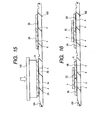
Next, as shown in Fig. 15, a heat tool (also called
heat block) 102 having a flat bottom is pushed onto the two
chips 2A and 2B. For example, the pushing pressure of the
heat tool 102 is 15 kg/10 mm2 and the heating temperature
is 235°C, whereby not only the resin tape 6a melts and the
gap between the chips 2A, 2B and the multi-wiring substrate
100 and the gap between the chips 2A and 2B are filled with
the under-fill resin 6, but also the Au bumps 4 on the
chips 2A, 2B and the wiring lines (not shown in Fig. 15) on
the multi-wiring substrate 100 are connected together
electrically. The under-fill resin 6 is formed for
protecting the main surfaces (the surfaces on which
semiconductor elements and electrodes (bonding pads) are
formed) of the chips 2A and 2B, for bonding the chips 2A
and 2B to the multi-wiring substrate 100, and for ensuring
a required strength of connection between the bump
electrodes 4 and the electrode pads on the multi-wiring
substrate 100.
Thus, in this embodiment, by melting the resin tape
6a formed almost equal in size to the chips 2A and 2B, the
gap between the chips 2A, 2B and the multi-wiring substrate
100 and the gap between the chips 2A and 2B are filled with
the under-fill resin 6. According to this method, for
example in comparison with a resin filling method wherein a
liquid under-fill resin is fed around the chips 2A and 2B
with use of a dispenser, it is possible to diminish the
amount of the under-fill resin 6 protruded to around the
chips 2A and 2B and therefore the bonding pads 9 on the
multi-wiring substrate 100, which are arranged so as to
surround the chips 2A and 2B, are not covered with the
under-fill resin 6.
Next, as shown in Figs. 16 and 17, a chip 2C is
mounted on the two chips 2A and 2B. As shown in Fig. 18,
bonding pads 13 are formed along the four sides of a main
surface of the chip 2C on which is formed a microprocessor.
The number of the bonding pads 13 is larger than that of
the bonding pads formed on the chips 2A and 2B. Thus, the
chip with a relatively small number of bonding pads is
mounted by a face-down method, while the chip with a
relatively large number of bonding pads is mounted by a
face-up method, whereby the wiring density (wiring pitch)
of the wiring substrate and the distribution of wiring are
decreased and it is possible to provide a high-density
package of low cost.
The chip 2C is disposed centrally of each package
substrate-forming area so that the Au wires 8 which connect
the multi-wiring substrate 100 and the chip 2C become as
uniform as possible in length. Further, a tape-like
adhesive 7 pre-cut to the same size as the chip 2C is
affixed to a back side of the chip 2C in the following
manner. As shown in Figs. 19 and 20, at the time of
affixing a dicing tape 15 to a back side of a wafer 14
after completion of the ordinary wafer process, the tape-like
adhesive 7 is sandwiched in between the wafer 14 and
the dicing tape 15 and in this state the wafer 14 is diced
to obtain the chip 2C. Thereafter, the dicing tape 15 is
removed from the back side of the chip 2C, whereby the
adhesive 7 of the same size as the chip 2C is left
unremoved on the back side of the chip 2C. As the adhesive
7 there is used a polyimide resin-based adhesive for
example.
Next, the multi-wiring substrate 100 is heated within
a heating furnace at 180°C for 1 hour or so, whereby the
adhesive 7 softens and the chip 2C is bonded onto the chips
2A and 2B.
Next, as shown in Figs. 21 and 22, the bonding pads 9
on the multi-wiring substrate 100 and the bonding pads 13
(not shown in Figs. 21 and 22) on the chip 2C are connected
together through Au wires 8. For example, the connection
of the Au wires 8 is performed by means of a wire bonder
which uses both ultrasonic oscillation and
thermocompression bonding.
Then, as shown in Figs. 23 and 24, the multi-wiring
substrate 100 is loaded into a molding die (not shown) and
the whole of the main surface of the multi-wiring substrate
100 is sealed with molding resin 3 at a time. The molding
resin is a thermosetting epoxy resin with silica dispersed
therein, the silica having a particle diameter of about 70
to 100 µm for example. As noted earlier, since the gap
between the chips 2A, 2B and the multi-wiring substrate 100
and the gap between the chips 2A and 2B are filled with the
under-fill resin 6 in advance, there is no fear of an air
pocket (void) being formed in those gaps when the main
surface of the multi-wiring substrate 100 is resin-sealed.
Next, as shown in Fig. 25, solder bumps 11 are
connected to the electrode pads 9 (not shown in Fig. 25)
formed on the back side of the multi-wiring substrate 100.
The connection of the solder bumps 11 is performed, for
example, by feeding solder balls of a low melting Pb-Sn
eutectic alloy to the surfaces of the electrode pads 9 and
by subsequently reflowing the solder balls.
Then, as shown in Fig. 26, the multi-wiring substrate
100 is diced into individual pieces along the dicing lines
L shown in Figs. 4 and 5, whereby the multi-chip module
(MCM) of this embodiment shown in Figs. 1 to 3 is completed.
When dicing the multi-wiring substrate 100, there is used a
dicing blade having a width smaller than the width of each
of the grooves 101 (see Figs. 6 and 7) formed in the dicing
lines L of the multi-wiring substrate 100. By so doing,
side faces of the package substrate 1 are partially covered
with the molding resin 3 (see Fig. 2), so that the amount
of moisture entering the side faces of the package
substrate 1 from the side faces thereof is decreased and
hence the reliability of the multi-chip module (MCM) is
improved. The multi-chip module (MCM) resulting from the
dicing process is mounted through the solder bumps 11 onto
a mounting substrate, e.g., a printed circuit board (PCB).
A method of manufacturing a semiconductor device
according to a second embodiment of the present invention
will be described below step by step with reference to Figs.
27 to 34.
In the previous first embodiment Au bumps 4 are
formed on the main surface of the chip 2A with a DRAM
formed thereon and also on the main surface of the chip 2B
with a flash memory formed thereon, but in this second
embodiment there are used solder bumps 20 instead of Au
bumps 4.
Fig. 27 is a plan view showing a state in which
solder bumps 20 are formed on a main surface of a chip 2A
with a DRAM formed thereon. As shown in the same figure,
the solder bumps 20 are arranged in the form of an array on
the main surface of the chip 2A. Bonding pads 13 and the
solder bumps 20 are electrically connected with each other
through Cu wiring lines 21 called re-wiring lines. The Cu
wiring lines 21 function as an interposer for converting
the pitch of the bonding pads 13 to the pitch of the solder
bumps 20, whereby the pitch of the solder bumps 20 can be
made wider than that of the bonding pads 13, so that the
expensive build-up substrate need not be used as the
package substrate 1 and it is possible to use a less
expensive resin substrate having a wide pitch of wiring
lines 5.
The Cu wiring lines 21 and the solder bumps 20 are
formed in the final step of the wafer process. That is,
after an organic insulating film such as a polyimide resin
film is formed on a surface protecting film of a wafer, Cu
wiring lines 21 are formed on the organic insulating film
by an electrolytic plating method for example. The Cu
wiring lines 21 and the bonding pads 13 are electrically
connected with each other through through-holes formed in
the organic insulating film on the bonding pads 13. The
solder bumps 20 are formed by printing solder paste to one
ends of the Cu wiring lines 21 by a screen printing method
and by subsequently heating the wafer to melt the solder
paste. For example, the solder bumps 20 are constituted by
a Pb-Sn alloy (liquidus line temperature: 320°C to 325°C)
including 2 wt% of Sn. Though not shown, Cu wiring lines
21 and solder bumps 20 are formed in the same manner also
on a main surface of a chip 2B with a flash memory formed
thereon.
Next, as shown in Fig. 28, the chips 2A and 2B are
positioned in each of package substrate-forming areas of a
multi-wiring substrate 100, then the multi-wiring substrate
100 is heated to about 340°C within an electric furnace to
reflow the solder bumps 20, thereby electrically connecting
the solder bumps 20 on the chips 2A and 2B with the wiring
lines 5 on the multi-wiring substrate 100.
Then, as shown in Fig. 29, a chip 2C is mounted on
the two chips 2A and 2B. As in the first embodiment,
bonding of the chip 2C with the chips 2A and 2B is
performed using an adhesive 7 affixed to a back side of the
chip 2C.
Next, as shown in Figs. 30 and 31, bonding pads 9 on
the multi-wiring substrate 100 and bonding pads 13 on the
chip 2C are connected together through Au wires 8. As in
the first embodiment, the connection of the Au wires 8 is
performed for example by means of a wire bonder which uses
both ultrasonic oscillation and thermocompression bonding.
Then, as shown in Fig. 32, a liquid under-fill resin
6 is fed to the peripheral portions of the chips 2A and 2B
with used of a dispenser or the like and is thereafter
heated and cured, whereby the gap between the chips 2A, 2B
and the multi-wiring substrate 100 and the gap between the
chips 2A and 2B are filled with the under-fill resin 6.
Since the liquid under-fill resin 6 is high in fluidity and
the particle diameter (about 3 µm) of the silica filler
added therein is smaller than the gap (about 20 to 100 µm)
between the chips 2A and 2B, the chip-to-chip gap can be
filled completely with the under-fill resin 6.
In this embodiment, when the liquid under-fill resin
6 is fed to the peripheral portions of the chips 2A and 2B,
it is also fed to the peripheral portions of the package
substrate-forming areas to cover the surfaces of the
bonding pads 13 with the under-fill resin 6. It is not
necessary for the under-fill resin 6 to cover the surfaces
of all the bonding pads 13 completely. If the under-fill
resin 6 is cured in this state, one end portions of the Au
wires 8 connected to the surfaces of the bonding pads 13
are fixed by the under-fill resin 6, so that the
reliability of connection between the bonding pads 13 and
the Au wires 8 is improved. Besides, since the wire
bonding process is completed before the injection of the
under-fill resin 6, it is possible, with the under-fill
resin 6, to avoid contamination of the electrode pads
formed on the substrate.
Next, as shown in Fig. 33, the multi-wiring substrate
100 is loaded into a molding die (not shown) and the whole
of a main surface thereof is sealed with a molding resin 3
at a time. The molding resin 3 is, for example, a
thermosetting epoxy resin with silica dispersed therein,
the silica having a particle diameter of about 70 to 100 µm.
As noted earlier, the gap between the chips 2A, 2B and the
multi-wiring substrate 100 and the gap between the chips 2A
and 2B are filled with the under-fill resin 6 beforehand,
there is no fear of an air pocket (void) being formed when
the main surface of the multi-wiring substrate 100 is
resin-sealed. In this embodiment, moreover, since one end
portions of the Au wires 8 are fixed to the surfaces of the
bonding pads 13 through the under-fill resin 6, it is
possible to surely prevent breaking of Au wires 8 caused by
pressure at the time of injection of melted molding resin 3
into the molding die.
Then, as shown in Fig. 34, the solder bumps 11 are
connected to electrode pads 10 formed on a back side of the
multi-wiring substrate 100. Though not shown, the multi-chip
module (MCM) of this embodiment is completed by dicing
the multi-wiring substrate 100 in the same manner as in the
first embodiment.
A method of manufacturing a semiconductor device
according to a third embodiment of the present invention
will be described below with reference to Figs. 35 to 37.
First, as shown in Fig. 35, solder bumps 20 on chips
2A, 2B and wiring lines 5 on a multi-wiring substrate 100
are electrically connected with each other, then a chip 2C
is mounted on the two chips 2A and 2B through an adhesive 7,
and thereafter bonding pads 9 on the multi-wiring substrate
100 and bonding pads 13 on the chip 2C are connected
together through Au wires 8. These steps are the same as
those shown in Figs. 27 to 31 in the previous second
embodiment.
Then, as shown in Fig. 36, the multi-wiring substrate
100 is loaded into a molding die (not shown) and the whole
of a main surface thereof is sealed with resin at a time.
At this time, in this embodiment there is used a molding
resin 3 with a silica filler added therein, the silica
filler having a particle diameter of about 3 µm, as is the
case with the under-fill resin 6 used in the previous first
and second embodiments. The particle diameter of the
silica filler added to the molding resin 3 is smaller than
the gap (about 20 to 100 µm) between the chips 2A and 2B,
so that the gap between the chips 2A, 2B and the multi-wiring
substrate 100, as well as the gap between the chips
2A and 2B, can be filled with the molding resin 3
completely. This molding resin 3 is expensive in
comparison with the molding resin 3 with silica of about 70
to 100 µm in particle diameter added therein which was used
in the first and second embodiments, but permits omission
of the step of injecting the under-fill resin 6 into the
gap between the chips 2A, 2B and the multi-wiring substrate
100 and the gap between the chips 2A and 2B.
Next, as shown in Fig. 37, solder bumps 11 are
connected to electrode pads 9 on a back side of the multi-wiring
substrate 100 in the same way as in the first and
second embodiments. Thereafter, though not shown, the
multi-wiring substrate 100 is diced in the same manner as
in the first and second embodiment to complete the multi-chip
module (MCM) of this embodiment.
Fig. 38 is a sectional view showing a semiconductor
device according to a fourth embodiment of the present
invention and Fig. 39 is a sectional view showing a part of
Fig. 38 on a larger scale.
In the semiconductor device of this embodiment is a
multi-chip module (MCM) wherein a chip 2A with a DRAM
formed thereon is mounted on a main surface of a package 1,
a chip 2C with a high-speed microprocessor (MPU) formed
thereon is stacked on the chip 2A, and the two chips 2A and
2C are sealed with a molding resin 3.
The underlying chip 2A is electrically connected to
wiring lines 5 on the package substrate 1 through Au bumps
4 formed on the main surface of the package substrate 1.
That is, the chip 2A is mounted in accordance with a flip-chip
method. A gap is formed between a main surface (lower
surface) of the chip 2A and the main surface of the package
substrate 1 and is filled with an under-fill resin 6.
The overlying chip 2C is bonded to an upper surface
of the chip 2A through an adhesive 7. Bonding pads 13
formed on a main surface of the chip 2C are electrically
connected to bonding pads 9 on the package substrate 1
through plural Au wires 8. That is, the chip 2C is mounted
in accordance with a wire bonding method.
As shown in Fig. 13, the chip 2A with a DRAM formed
thereon has a rectangular shape in plan and plural Au bumps
4 are arranged in a row centrally of the main surface of
the chip 2A. The chip 2C with a microprocessor formed
thereon has a generally square shape in plan and bonding
pads 13 are formed along the four sides of the main surface
of the chip 2C. The number of bonding pads 13 formed on
the chip 2C is larger than the number of bonding pads (Au
bumps 4) formed on the chip 2A.
As noted earlier, when the chip 2A having a small
number of bonding pads and a large minimum pitch of bonding
pads and the chip 2C having a large number of bonding pads
and a small minimum pitch of bonding pads are to be stacked
one on the other, the chip 2A having a large minimum pitch
of bonding pads is face-down mounted through Au bumps 4,
while the chip 2C having a small minimum pitch of bonding
pads is face-up mounted by wire bonding. By so doing, the
requirement for the wiring density of the package substrate
1 can be eased, so that it becomes possible to use a less
expensive substrate as the package substrate 1 and provide
a package of a low cost and which permits a high-density
packaging.
As shown in Fig. 39, when the chip 2C having a
generally square plan shape is stacked on such a single
chip 2A having a rectangular plan shape as noted above,
there sometimes occurs a case where the peripheral portion
of the overlying chip 2C protrudes outwards (overhangs)
from the peripheral portion of the underlying chip 2A.
In this case, if the overhanging quantity of the
overlying chip 2C is large, there is a fear that the chip
2C may be cracked under a load applied to the peripheral
portion of the chip 2C at the time of bonding Au wires 13
onto the bonding pads 13 formed in the peripheral portion
of the chip 2C. As a countermeasure there is proposed a
method wherein the amount of the resin injected into the
gap between the underlying chip and the substrate is
increased to let the resin be injected also just under the
peripheral portion of the chip 2C (Japanese Unexamined
Patent Publication No. 2000-299431). According to this
method, even if a load is applied to the peripheral portion
of the overlying chip 2C in wire bonding, it is possible to
prevent cracking of the chip 2C because the peripheral
portion of the chip 2C is supported with resin.
According to the above countermeasure, however, since
the overhanging quantity of the under-fill resin 6 from the
underlying chip 2A to the outer periphery thereof is
controlled by controlling the amount of the same resin fed,
it is difficult to control the overhanging quantity
accurately. Particularly, if the bonding pads on the main
surface of the package substrate 1 are contaminated by
excess overhanging of the under-fill resin 6, there is a
fear that a disconnection defect between the bonding wires
and the bonding pads 9 may occur in the subsequent wire
bonding step. For solving such a problem, that is, for
preventing contamination of the bonding pads 9 even with
excess overhanging of the under-fill resin 6, if an attempt
is made to ensure a sufficient distance from the area where
the bonding pads 13 of the overlying chip 2C are arranged
up to the bonding pads 9, this attempt leads to an increase
in size of the package substrate 1 and hence of the MCM,
which is not desirable.
In this embodiment, as shown in Fig. 39, for avoiding
contamination of the bonding pads 9 even when there are
variations in the overhanging quantity of the under-fill
resin 6, there is adopted a construction wherein the
bonding pads 13 of the overlying chip 2C are not supported
by the overhanging portion of the under-fill resin 6 in the
case where the overlying chip 2C overhangs outside the
underlying chip 2A. Further, for avoiding crack of the
overlying chip 2C in the wire bonding step, the length (h)
of an unsupported portion of the overlying chip 2C is set
at a value of not larger than 1.5 mm, preferably not larger
than 1 mm.
Fig. 40 is a layout diagram of pins (terminals) of
the multi-chip module (MCM) according to this embodiment.
The package substrate 1 used in the multi-chip module
(MCM) of this embodiment has a pin layout common to a
package substrate designed for mounting a single chip 2C
with a high-speed microprocessor formed thereon. Therefore,
out of the pins shown in Fig. 40, control pins (CASL, RASL,
CS3, RDWR, WE1, WE0, all of which will hereinafter be
referred to as "C"), address pins (A0 to A14, all "A"
hereinafter), and data pins (D0 to D15, all "D"
hereinafter), are connected using common wiring lines 5.
In case of constituting the multi-chip module (MCM)
by mounting the chip 2A in addition to the chip 2C, it is
necessary for the package substrate 1 to be provided with
pins (two or so in the case of DRAM) for testing
characteristics of the chip 2A in addition to pins for
testing electric characteristics of the chip 2C. In this
embodiment, therefore, as shown in Fig. 41, test pins 11t
for the chip 2A are arranged just under the chip mounting
area.
In this case, if the test pins 11t are arranged near
the center of the package substrate 1, the wiring lines 5
connected to the test pins become longer and hence the
wiring design for the package substrate 1 becomes difficult.
On the other hand, in order to make shortest the length of
the wiring lines 5 connected to the test pins 11t, if the
test pins 11t are arranged in adjacency to the area where
other pins (solder bumps 11) are arranged, the distance
between the other pins (solder bumps 11) and the test pins
11t becomes shorter, so that it becomes difficult to make
layout of the wiring lines 5 connected to other pins which
are adjacent to the test pins 11t; in this case, it becomes
difficult to make wiring design for the mounting substrate
which is for mounting the MCM.
For solving the above-mentioned problem, as shown in
Fig. 41, the test pins 11t should not be arranged in
adjacency to the area where other pins (solder bumps 11)
are arranged, but it is preferable that the test pins 11t
be arranged inside the other pins through a spacing of one
row. In the case where two or more non-connection pins are
included in the other pins (solder bumps 11), the test pins
11t may be arranged in the area where the non-connection
pins are arranged.
Thus, the multi-chip module (MCM) is constituted
using the package substrate 1 having a pin layout
(exclusive of the test pins 11t) common to the package
substrate which is designed for mounting a single chip 1C
with a high-speed microprocessor (MPU) formed thereon.
With this construction, it is possible to reduce the design
cost of the package substrate 1, and also to improve ease
in handling the package substitute 1.
Fig. 42 illustrates a layout of a group of address
pins (A) and a group of data pins (D) on the package
substrate 1. As shown in the same figure, in the package
substrate 1 for packaging the chip 2C having a large number
of pins, like a high-speed microprocessor (MPU), generally
address pins (A) are concentrated in a specific area and so
are data pins (D), further, the group of address pins (A)
and the group of data pins (D) are arranged adjacent each
other, whereby it is possible to shorten the wiring length
for example when the package substrate 1 is connected to an
external memory chip.
On the other hand, in the chip 2A with a DRAM formed
thereon, generally a group of address pins (A) is disposed
on one end side and a group of data pins (D) is disposed on
an opposite end side in the longitudinal direction of the
chip 2A, as shown in Fig. 43.
Therefore, in case of constituting the multi-chip
module (MCM) by stacking the chip 2C on the chip 2A as in
this embodiment, it is preferable for the chip 2A to be
oriented so that a group of address pins (A) on the package
substrate 1 and a group of address pins (A) on the chip 2A
are arranged adjacent each other and so are a group of data
pins (D) on the package substrate 1 and a group of data
pins (D) on the chip 2A, as shown in Fig. 44.
According to such a layout, a group of wiring lines 5
for connection between the group of address pins (A) on the
package substrate 1 and the group of address pins on the
chip 2A and a group of wiring lines 5 for connection
between the group of data pins (D) on the package substrate
1 and the group of data pins (D) on the chip 2A can be
prevented from crossing each other and therefore the wiring
design of the package substrate 1 becomes easier.
Figs. 45(a) to (c) show a layout example of a group
of address pins (A) and a group of data pins (D) on the
package substrate 1, in which the area indicated with
symbol (D>A) represents an area in which data pins (D) are
mainly arranged, while the area indicated with symbol (A>D)
represents an area in which address pins (A) are mainly
arranged. In these examples, if the chip 2A with a DRAM
formed thereon is oriented as illustrated in the figures, a
group of wiring lines 5 for connection between a group of
address pins (A) on the package substrate 1 and a group of
address pins (A) on the chip 2A and a group of wiring lines
5 for connection between a group of data pins (D) on the
package substrate 1 and a group of data pins (D) on the
chip 2A can be prevented from crossing each other on the
package substrate 1.
In the multi-chip module (MCM) of this embodiment the
chip 2C is stacked on the chip 2A with a DRAM formed
thereon, but also in case of constituting a multi-chip
module (MCM) by stacking the chip 2C on the chip 2B with a
flash memory formed thereon, as shown in Fig. 14 for
example, it is preferable that the chip 2B be oriented in
the same manner as above.
More specifically, generally in the chip 2B with a
flash memory formed thereon like that shown in Fig. 14, a
group of address pins (A) is disposed along one of two
short sides opposed to each other and a group of data pin
(D) is disposed along the other short side. Therefore,
also in this case, the chip 2B is oriented so that a group
of address pins (A) on the package substrate 1 and a group
of address pins (A) on the chip 2B are arranged adjacent
each other and so are a group of data pins (D) on the
package substrate 1 and a group of data pins (D)O on the
chip 2B, whereby a group of wiring lines 5 for connection
between the group of address pins (A) on the package
substrate 1 and a group of address pins (A) on the chip 2B
and a group of wiring lines 5 for connection between the
group of data pins (D) on the package substrate 1 and the
group of data pins (D) on the chip 2B can be prevented from
crossing each other on the package substrate 1.
In case of stacking the chip 2C with a high-speed
microprocessor (MPU) formed thereon onto both chip 2A with
a DRAM formed thereon and chip 2B with a flash memory
formed thereon, like the multi-chip module (MCM) of the
first embodiment, there sometimes occurs a case where the
center of both chips 2A and 2B serving as a base of the MPU
chip 2C does not coincide with the center of the package
substrate 1. Usually, in case of'stacking chips on a
wiring substrate, a chip to be stacked is aligned with a
base chip. However, if the MPU chip 2C which is larger in
the number of pins and smaller in the minimum bonding pad
pitch than the DRAM chip 2A and flash chip 2B is offset
from the center of the module substrate 1 in an effort to
be aligned with the center of the underlying chips, there
arise problems such as the bonding wires being non-uniform
in length.
More particularly, the number of bonding pads 9 on
the module substrate 1 necessary for the connection thereof
with the MPU chip 2C is very large, so by arranging the
bonding pads 9 along the outer periphery of the module
substrate 1, it is possible to ensure a required spacing of
the bonding pads 9. However, the greater the degree of
offset of the MPU chip 2C from the module substrate 1, the
more irregular the distance between the bonding pads 13
arranged along the outer periphery of the MPU chip 2C and
the bonding pads 9 on the module substrate 1, so that the
bonding wires 8 become irregular in length and there is a
fear of occurrence of problems such as wire deformation at
the time of sealing with resin and short-circuit
particularly in longer portions of the bonding wires 8.
For solving these problems and for making uniform the
distance between the bonding pads 13 and the bonding pads 9
in a misaligned state of the MPU chip 2C with the module
substrate 1, it is necessary to narrow the spacing of the
bonding pads 9 so that the bonding pads 9 are received on
the main surface of the module substrate 1 or increase the
size of the module substrate 1 so that all of the bonding
pads 9 can be arranged thereon.
Therefore, also in case of arranging the chip 2C on
the chips 2A and 2B which are arranged at positions
deviated from the center of the substrate, if the number of
pins on the chip 2C is large in comparison with the chips
2A and 2B and if it is necessary to loosen the pitch of
bonding pads 9 corresponding to the pitch C, it is
desirable to stack the chip 2C so as to approximate its
center to the center of the package substrate 1 rather than
to the center of the chip 2A.
Although the present invention has been described
concretely on the basis of the above embodiments, it goes
without saying that the present invention is not limited to
the above embodiments, but that various changes may be made
within the scope not departing from the gist of the
invention.
For example, in case of combining a single chip 2A
with DRAM formed thereon with a single chip 2C with MPU
formed thereon to constitute a multi-chip module (MCM), for
example as in the above fourth embodiment, there may-be
adopted such a method as shown in Fig. 46 wherein a single
chip 2A with DRAM formed thereon and a dummy chip 2D are
arranged side by side on the main surface of the package
substrate 1 and the chip 2C is stacked on the two chips 2A
and 2D. In this case, the dummy chip 2D is formed, for
example, by dicing a mirror polish wafer not formed with an
integrated circuit and by equalizing its thickness to the
sum of the thickness of chip 2A and the height of Au bumps
4. Such a mounting method is effective for example in the
case where an outside diameter of the overlying chip 2C is
much larger than that of the underlying chip 2A and the
overhanging quantity (h) of the overlying chip 2C relative
to the underlying chip 2A described in connection with Fig.
39 cannot be set at a value of 1.5 mm or less.
The chip mounted on the package substrate by the
flip-chip method is not limited to DRAM alone, flash memory
alone, or a combination of DRAM and flash memory. Various
memory chips may be combined arbitrarily such as DRAMs with
each other, flash memories with each other, or a
combination of DRAM or flash memory with SRAM (Static
Random Access Memory). Also as to the chip to be stacked
on the memory chips, no limitation is made to a
microprocessor or ASIC, but there may be used a chip formed
with LSI of a narrower pitch than memory chips. Further,
the number of chips mounted on the package substrate is not
limited to two or three.
On the package substrate there may be mounted other
small-sized electronic parts than chips, such as capacitors
and resistors. For example, by mounting a chip capacitor
along the outer periphery of a memory chip, it is possible
to diminish noise produced during operation of the memory
chip and thereby attain a high-speed operation.
Further, various design modifications may be made
within the scope not departing from the gist of the present
invention, such as using a build-up substrate as a chip
packaging substrate or attaching a heat dissipating cap to
a part of the package substrate.
According to one preferred mode for carrying out the
present invention it is possible to improve the reliability
of a multi-chip module wherein on plural chips is stacked
another chip and the chips are sealed with resin.
According to another preferred mode for carrying out
the present invention it is possible to reduce the
manufacturing cost of a multi-chip module wherein on plural
chips is stacked another chip and the chips are sealed with
resin.
Claims (37)
- A method of manufacturing a semiconductor device, comprising the steps of:(a) providing a wiring substrate having a plurality of wiring lines over a main surface thereof;(b) providing a first semiconductor chip and a second semiconductor chip each having over a main surface thereof a plurality of semiconductor elements and a plurality of electrodes;(c) mounting the first semiconductor chip over the main surface of the wiring substrate through a plurality of first bump electrodes in such a manner that the main surface thereof is opposed to the main surface of the wiring substrate;(d) mounting the second semiconductor chip over the main surface of the wiring substrate through a plurality of second bump electrodes in such a manner that the main surface thereof is opposed to the main surface of the wiring substrate and that one side faces of the first and the second semiconductor chips are adjacent to each other;(e) filling an area with a first resin which area is defined by the adjacent one side faces of the first and the second semiconductor chips and the main surface of the wiring substrate; and(f) after the step (e), sealing the first and the second semiconductor chips with a second resin.
- A method according to claim 1,
wherein in the steps (c) and (d), the first and the second semiconductor chips are bonded using a tape-like resin disposed between the main surface of the wiring substrate and the main surfaces of the first and the second semiconductor chips, and
wherein the first resin used in the step (e) is a part of the tape-like resin. - A method according to claim 1, further comprising, after the step (e) and before the step (f), a step of stacking a third semiconductor chip over the first and the second semiconductor chips so as to cover the area defined by the adjacent one side faces of the first and the second semiconductor chips and the main surface of the wiring substrate.
- A method according to claim 1, further comprising:wherein the third semiconductor chip has on a main surface thereof a plurality of semiconductor elements and a plurality of electrodes and is stacked over the first and the second semiconductor chips in such a manner that a back side thereof is opposed to back sides of the first and the second semiconductor chips,a step of stacking a third semiconductor chip over the first and the second semiconductor chips after the step (e) and before the step (f),
wherein the wiring substrate further has a plurality of electrode pads for electric connection with the plural electrodes of the third semiconductor chip, the electrode pads being arranged around the first and the second semiconductor chips, and
wherein there is included a step of connecting the plural electrode pads of the wiring substrate and the plural electrodes of the third semiconductor chip with each other through bonding wires. - A method of manufacturing a semiconductor device, comprising the steps of:wherein the wiring substrate further has a plurality of electrode pads arranged around the first semiconductor chip, and(a) providing a wiring substrate having a plurality of wiring lines over a main surface thereof;(b) providing a first semiconductor chip having, over a main surface thereof, a plurality of semiconductor elements and a plurality of bump electrodes, and a second semiconductor chip having, over a main surface thereof, a plurality of semiconductor elements and a plurality of electrodes;(c) mounting the first semiconductor chip over the main surface of the wiring substrate through the plural bump electrodes in such a manner that the main surface thereof is opposed to the main surface of the wiring substrate, and bonding the main surface of the first semiconductor chip and the main surface of the wiring substrate with each other through a tape-like resin;(d) stacking the second semiconductor chip over the first semiconductor chip in such a manner that a back side of the first semiconductor chip is opposed to a back side of the second semiconductor chip;(e) connecting the plural wiring lines of the wiring substrate and the plural electrodes of the third semiconductor chip with each other through a plurality of bonding wires; and(f) sealing the first and the second semiconductor chips and the plural bonding wires with resin,
wherein one end portions of the plural bonding wires are connected to corresponding the plural electrode pads of the wiring substrate. - A method of manufacturing a semiconductor device, comprising the steps of:(a) providing a wiring substrate having a plurality of wiring lines over a main surface thereof;(b) providing a first semiconductor chip having, over a main surface thereof, a plurality of semiconductor elements and a plurality of first bump electrodes, a second semiconductor chip having, over a main surface thereof, a plurality of semiconductor elements and a plurality of second bump electrodes, and a third semiconductor chip having, over a'main surface thereof, a plurality of semiconductor elements and a plurality of electrodes;(c) mounting the first semiconductor chip over the main surface of the wiring substrate through the plural first bump electrodes in such a manner that the main surface thereof is opposed to the main surface of the wiring substrate, and bonding the main surface of the first semiconductor chip and the main surface of the wiring substrate with each other through a tape-like adhesive;(d) mounting the second semiconductor chip over the main surface of the wiring substrate through the plural second bump electrodes in such a manner that the main surface thereof is opposed to the main surface of the wiring substrate and that one side faces of the first and the second semiconductor chips are adjacent to each other, and bonding the main surface of the second semiconductor chip and the main surface of the wiring substrate with each other through a tape-like resin;(e) pushing a heating block in the direction of the main surface of the wiring substrate after the step (d) and with the heating block contacted with back sides of the first and the second semiconductor chips; and(f) after the step (e), stacking the third semiconductor chip over the first and the second semiconductor chips in such a manner that the back sides of the first and the second semiconductor chips and a back side of the third semiconductor chip are opposed to each other.
- A method of manufacturing a semiconductor device, comprising the steps of:(a) providing a wiring substrate having, over a main surface thereof, a plurality of wiring lines and a plurality of electrode pads;(b) providing a first semiconductor chip having, over a main surface thereof, a plurality of semiconductor elements and a plurality of bump electrodes, and a second semiconductor chip having, over a main surface thereof, a plurality of semiconductor elements and a plurality of electrodes;(c) mounting the first semiconductor chip over the main surface of the wiring substrate through the plural bump electrodes in such a manner that the main surface thereof is opposed to the main surface of the wiring substrate;(d) stacking the second semiconductor chip over the first semiconductor chip in such a manner that a back side of the first semiconductor chip and a back side of the second semiconductor chip are opposed to each other;(e) connecting the plural electrode pads of the wiring substrate and the plural electrodes of the second semiconductor chip with each other through a plurality of bonding wires;(f) after the step (e), injecting a first resin between the main surface of the first semiconductor chip and the main surface of the wiring substrate; and(g) after the step (f), sealing the first and the second semiconductor chips and the plural bonding wires with a second resin.
- A semiconductor device comprising:wherein the plural electrode pads of the wiring substrate is disposed between the first semiconductor chip and a first side of the wiring substrate and also between the second semiconductor chip and a second side of the wiring substrate opposed to the first side, and(a) a wiring substrate of a square shape having, over a main surface thereof, a plurality of wiring lines and a plurality of electrode pads;(b) a first semiconductor chip of a square shape having, over a main surface thereof, a plurality of semiconductor elements and a plurality of electrodes, the first semiconductor chip being mounted over the main surface of the wiring substrate through a plurality of first bump electrodes in such a manner that the main surface thereof is opposed to the main surface of the wiring substrate;(c) a second semiconductor chip of a square shape having, over a main surface thereof, a plurality of semiconductor elements and a plurality of electrodes, the second semiconductor chip being mounted over the main surface of the wiring substrate through a plurality of second bump electrodes in such a manner that the main surface thereof is opposed to the main surface of the wiring substrate and that one side face thereof and one side face of the first semiconductor chip are adjacent to each other;(d) a third semiconductor chip having, over a main surface thereof, a plurality of semiconductor elements and a plurality of electrodes, the third semiconductor chip being stacked over the first and the second semiconductor chips in such a manner that a back side thereof is opposed to back sides of the first and the second semiconductor chips;(e) a plurality of bonding wires for electrically connecting the plural electrode pads of the wiring substrate and the plural electrodes of the third semiconductor chip with each other; and(f) a resin member for sealing the first, second and third semiconductor chips and the plural bonding wires,
wherein the distance between one mutually adjacent side faces of the first and the second semiconductor chips is shorter than the distance between the first semiconductor chip and the first side of the wiring substrate and the distance between the second semiconductor chip and the second side of the wiring substrate. - A semiconductor device comprising:wherein the pitch between the plural electrodes of the first semiconductor chip is larger than that between the plural electrodes of the second semiconductor chip.(a) a wiring substrate having over a main surface thereof a plurality of wiring lines and a plurality of electrode pads;(b) a first semiconductor chip having over a main surface thereof a plurality of semiconductor elements and a plurality of electrodes, the first semiconductor chip being mounted over the main surface of the wiring substrate through a plurality of bump electrodes in such a manner that the main surface thereof is opposed to the main surface of the wiring substrate;(c) a second semiconductor chip having, over a main surface thereof, a plurality of semiconductor elements and a plurality of electrodes, the second semiconductor chip being stacked over the first semiconductor chip in such a manner that a back side thereof is opposed to a back side of the first semiconductor chip;(d) a plurality of bonding wires for electrically connecting the plural electrode pads of the wiring substrate and the plural electrodes of the second semiconductor chip with each other; and(e) a resin member for sealing the first and the second semiconductor chips and the plural bonding wires,
- A semiconductor device comprising:wherein the pitch between the plural bump electrodes is larger than that between the plural electrodes of the second semiconductor chip.(a) a wiring substrate having over a main surface thereof a plurality of wiring lines and a plurality of electrode pads;(b) a first semiconductor chip having, over a main surface thereof, a plurality of semiconductor elements and a plurality of electrodes, the first semiconductor chip being mounted over the main surface of the wiring substrate through a plurality of bump electrodes in such a manner that a main surface thereof is opposed to the main surface of the wiring substrate;(c) a second semiconductor chip having over a main surface thereof a plurality of semiconductor elements and a plurality of electrodes, the second semiconductor chip being stacked over the first semiconductor chip in such a manner that a back side thereof is opposed to a back side of the first semiconductor chip;(d) a plurality of bonding wires for electrically connecting the plural electrode pads of the wiring substrate and the plural electrodes of the second semiconductor chip with each other; and(e) a resin member for sealing the first and the second semiconductor chips and the plural bonding wires,
- A method of manufacturing a semiconductor device, comprising the steps of:(a) providing a multi-wiring substrate, a first semiconductor chip having a plurality of first bump electrodes over a main surface thereof, a second semiconductor chip having a plurality of second bump electrodes over a main surface thereof, and a third semiconductor chip, the multi-wiring substrate having a main surface partitioned into a plurality of wiring substrate-forming areas, with a plurality of wiring lines and a plurality of electrode pads being formed in each of the plural wiring substrate-forming areas;(b) disposing the first semiconductor chip in each of first areas in the plural wiring substrate-forming areas in such a manner that the main surface thereof is opposed to the main surface of the multi-wiring substrate, disposing the second semiconductor chip in each of second areas in the plural wiring substrate-forming areas in such a manner that the main surface thereof is opposed to the main surface of the multi-wiring substrate, thereby electrically connecting the first semiconductor chip and the wiring lines of the multi-wiring substrate with each other through the plural first bump electrodes, and electrically connecting the second semiconductor chip and the wiring lines of the multi-wiring substrate with each other through the plural second bump electrodes;(c) injecting a first resin into a gap between the first and the second semiconductor chips and the multi-wiring substrate and also into a gap between the first and the second semiconductor chips;(d) stacking the third semiconductor chip over the first and the second semiconductor chips in such a manner that a back side thereof is opposed to the first and the second semiconductor chips, and thereafter electrically connecting the third semiconductor chip and the electrode pads of the multi-wiring substrate with each other through a plurality of wires;(e) sealing the first, second and third semiconductor chips mounted over the main surface of the multi-wiring substrate with a second sealing resin; and(f) dicing the multi-wiring substrate along boundary portions of the plural wiring substrate-forming areas to afford wiring substrates, each of the wiring substrates having the first, second and third semiconductor chips mounted over a main surface thereof.
- A method according to claim 11, wherein grooves are formed respectively along the boundary portions of the plural wiring substrate-forming areas.
- A method according to claim 12, wherein the dicing of the boundary portions of the multi-wiring substrate in the step (f) is carried out inside each of the grooves and at a width narrower than the width of each of the grooves.
- A method according to claim 1,
wherein the first resin contains a first silica filler, the first silica filler having a particle diameter smaller than the distance between the adjacent one side faces of the first and the second semiconductor chips, and
wherein the second resin contains a second silica filler, the second silica filler having a particle diameter larger than the distance between the adjacent one side faces of the first and the second semiconductor chips. - A method according to claim 1,
wherein the first resin does not contain any filler as an additive, and
wherein the second resin contains a silica filler, the silica filler having a particle diameter larger than the distance between the adjacent one side faces of the first and the second semiconductor chips. - A method according to claim 1, wherein the first and the second bump electrodes are Au bumps.
- A semiconductor device according to claim 9, wherein the plural electrodes of each of the first and the second semiconductor chips are plural bonding pads arranged at a predetermined spacing over the main surface of each of the first and the second semiconductor chips, and the plural bump electrodes are arranged over corresponding the plural bonding pads.
- A semiconductor device according to claim 17, wherein the plural bump electrodes are Au bumps.
- A semiconductor device according to claim 10,
wherein the plural electrodes of each of the first and the second semiconductor chips are plural bonding pads arranged at a predetermined spacing over the main surface of each of the first and the second semiconductor chips,
wherein the plural bump electrodes of the first semiconductor chip are electrically connected to corresponding the plural bonding pads through a plurality of wiring layers formed over the main surface of the first semiconductor chip, and
wherein the pitch between the plural bump electrodes is larger than the spacing between the plural bonding pads of the first semiconductor chip. - A semiconductor device according to claim 19, wherein the plural bump electrodes are solder bumps.
- A semiconductor device according to claim 17, wherein the number of electrodes of the first semiconductor chip is smaller than that of the second semiconductor chip.
- A semiconductor device according to claim 19, wherein the number of electrodes of the first semiconductor chip is smaller than that of the second semiconductor chip.
- A method according to claim 1, further comprising a step of forming a plurality of third bump electrodes on a back side opposed to the main surface of the wiring substrate.
- A semiconductor device comprising:wherein the number of the plural electrodes of the second semiconductor chip is larger than that of the first semiconductor chip.(a) a wiring substrate having, over a main surface thereof, a plurality of wiring lines and a plurality of electrode pads;(b) a first semiconductor chip having, over a main surface thereof, a plurality of semiconductor elements and a plurality of electrodes, the first semiconductor chip being mounted over the main surface of the wiring substrate through a plurality of bump electrodes in such a manner that the main surface thereof is opposed to the main surface of the wiring substrate;(c) a second semiconductor chip having, over a main surface thereof, a plurality of semiconductor elements and a plurality of electrodes, the second semiconductor chip being mounted in such a manner that a back side thereof is opposed to a back side of the first semiconductor chip;(d) a plurality of bonding wires for electrically connecting the plural electrode pads of the wiring substrate and the plural electrodes of the second semiconductor chip with each other; and(e) a resin member for sealing the first and the second semiconductor chips and the plural bonding wires,
- A method of manufacturing a semiconductor device, comprising the steps of:wherein in boundary portions of the plural wiring substrate-forming areas, the multi-wiring substrate has grooves formed in the depth direction from the main surface thereof, and(a) providing a multi-wiring substrate having a main surface partitioned into a plurality of wiring substrate-forming areas, with a plurality of wiring lines and a plurality of electrode pads being formed in each of the plural wiring substrate-forming areas, and a plurality of semiconductor chips, with a plurality of semiconductor elements and a plurality of electrodes being formed over a main surface of each of the plural semiconductor chips;(b) mounting a first semiconductor chip in each of the plural wiring substrate-forming areas;(c) electrically connecting the plural electrodes of the semiconductor chips and the wiring lines of the multi-wiring substrate with each other;(d) subjecting the semiconductor chips mounted respectively in the plural wiring substrate-forming areas to an electric test;(e) sealing the plural semiconductor chips mounted over the main surface of the multi-wiring substrate with resin; and(f) after the step (e), dicing the resin-sealed multi-wiring substrate along boundary portions of the plural wiring substrate-forming areas to afford wiring substrates with the semiconductor chips mounted over main surfaces thereof,
wherein in the grooves, a part of the plural wiring lines of the multi-wiring substrate is cut off, the grooves being formed before the step (d). - A method according to claim 25, wherein a part of the plural wiring lines of the multi-wiring substrate terminates at side faces of the grooves.
- A method according to claim 9, wherein the first semiconductor chip includes a memory circuit having a plurality of memory elements, and the second semiconductor chip includes a processor circuit adapted to operate in accordance with a program.
- A method according to claim 10, wherein the first semiconductor chip includes a memory circuit having a plurality of memory elements, and the second semiconductor chip includes a processor circuit adapted to operate in accordance with a program.
- A semiconductor device comprising:wherein the second semiconductor chip is stacked over the first semiconductor chip in such a manner that at least a part thereof overhangs the first semiconductor chip outwards, the overhanging quantity of the second semiconductor chip relative to the first semiconductor chip being not larger than 1.5 mm.(a) a wiring substrate having, over a main surface thereof, a plurality of wiring lines and a plurality of electrode pads;(b) a first semiconductor chip having, over a main surface thereof, a plurality of semiconductor elements and a plurality of electrodes, the first semiconductor chip being mounted over the main surface of the wiring substrate through a plurality of bump electrodes in such a manner that the main surface thereof is opposed to the main surface of the wiring substrate;(c) a second semiconductor chip having, over a main surface thereof, a plurality of semiconductor elements and a plurality of electrodes, the second semiconductor chip being stacked over the first semiconductor chip in such a manner that a back side thereof is opposed to a back side of the first semiconductor chip;(d) a plurality of bonding wires for electrically connecting the plural electrode pads of the wiring substrate and the plural electrodes of the second semiconductor chip with each other; and(e) a resin member for sealing the first and the second semiconductor chips and the plural bonding wires,
- A semiconductor device according to claim 29, wherein the overhanging quantity of the second semiconductor chip relative to the first semiconductor chip is not larger than 1 mm.
- A semiconductor device according to claim 29, wherein resin is injected into a gap between the main surface of the wiring substrate and the main surface of the first semiconductor chip.
- A semiconductor device comprising:wherein the layout of terminals of the multi-wiring substrate is the same as that of a wiring substrate designed for mounting only the first semiconductor chip.(a) a multi-wiring substrate having, over a main surface thereof, a plurality of wiring lines and a plurality of electrode pads;(b) a first semiconductor chip having, over a main surface thereof, a plurality of semiconductor elements and a plurality of electrode pads, the first semiconductor chip being mounted over the main surface of the multi-wiring substrate through a plurality of bump electrodes in such a manner that the main surface thereof is opposed to the main surface of the multi-wiring substrate;(c) a second semiconductor chip having, over a main surface thereof, a plurality of semiconductor elements and a plurality of electrodes, the second semiconductor chip being stacked over the first semiconductor chip in such a manner that a back side thereof is opposed to a back side of the first semiconductor chip;(d) a plurality of bonding wires for electrically connecting the plural electrode pads of the multi-wiring substrate and the plural electrodes of the second semiconductor chip with each other; and(e) a resin member for sealing the first and the second semiconductor chips and the plural bonding wires,
- A semiconductor device according to claim 32, wherein the multi-wiring substrate further has a testing terminal for testing electric characteristics of the second semiconductor chip, the testing terminal being provided at a position where a non-connection terminal of the first semiconductor chip is disposed.
- A semiconductor device according to claim 33, wherein the testing terminal is provided inside an innermost terminal row out of matrix terminal rows formed on the multi-wiring substrate, through a spacing of one row.
- A semiconductor device comprising:wherein the second semiconductor chip is stacked over the first semiconductor chip in such a manner that a central position thereof is coincident with a central position of the wiring substrate.(a) a wiring substrate having, over a main surface thereof, a plurality of wiring lines and a plurality of electrode pads;(b) a first semiconductor chip having, over a main surface thereof, a plurality of semiconductor elements and a plurality of electrodes, the first semiconductor chip being mounted over the main surface of the wiring substrate through a plurality of bump electrodes in such a manner that the main surface thereof is opposed to the main surface of the wiring substrate;(c) a second semiconductor chip having, over a main surface thereof, a plurality of semiconductor elements and a plurality of electrodes, the second semiconductor chip being stacked over the first semiconductor chip in such a manner that a back side thereof is opposed to a back side of the first semiconductor chip;(d) a plurality of bonding wires for electrically connecting the plural electrode pads of the wiring substrate and the plural electrodes of the second semiconductor chip with each other; and(e) a resin member for sealing the first and the second semiconductor chips and the plural bonding wires,
- A semiconductor device comprising:wherein the wiring substrate further has a first area in which a plurality of address terminals are mainly concentrated and a second area adjacent to the first area and in which a plurality of data terminals are mainly concentrated,(a) a wiring substrate having, over a main surface thereof, a plurality of wiring lines and a plurality of electrode pads;(b) a first semiconductor chip having, over a mains surface thereof, a plurality of semiconductor elements and a plurality of electrodes, the first semiconductor chip being mounted over the main surface of the wiring substrate through a plurality of bump electrodes in such a manner that the main surface thereof is opposed to the main surface of the wiring substrate;(c) a second semiconductor chip having, over a main surface thereof, a plurality of semiconductor elements and a plurality of electrodes, the second semiconductor chip being stacked over the first semiconductor chip in such a manner that a back side thereof is opposed to a back side of the first semiconductor chip;(d) a plurality of bonding wires for electrically connecting the plural electrode pads of the wiring substrate and the plural electrodes of the second semiconductor chip with each other; and(e) a resin member for sealing the first and the second semiconductor chips and the plural bonding wires,
wherein on one end side of the main surface of the first semiconductor chip are mainly concentrated a plurality of address terminals, while on an opposite end side of the main surface of the first semiconductor chip are mainly concentrated a plurality of data terminals, and
wherein the first semiconductor chip mounted over the main surface of the wiring substrate is oriented so that one end side of the first semiconductor chip with the plural address terminals concentrated thereon and the first area of the wiring substrate with the plural address terminals concentrated therein are in proximity to each other, and the opposite end side of the first semiconductor chip with the plural data terminals concentrated thereon and the second area of the wiring substrate with the plural data terminals concentrated therein are in proximity to each other. - A semiconductor device according to claim 36, wherein a DRAM or a flash memory is formed on the main surface of the first semiconductor chip.
Applications Claiming Priority (3)
| Application Number | Priority Date | Filing Date | Title |
|---|---|---|---|
| JP2001172503 | 2001-06-07 | ||
| JP2001172503 | 2001-06-07 | ||
| PCT/JP2002/003434 WO2002103793A1 (en) | 2001-06-07 | 2002-04-05 | Semiconductor device and manufacturing method thereof |
Publications (2)
| Publication Number | Publication Date |
|---|---|
| EP1401020A1 true EP1401020A1 (en) | 2004-03-24 |
| EP1401020A4 EP1401020A4 (en) | 2007-12-19 |
Family
ID=19014112
Family Applications (1)
| Application Number | Title | Priority Date | Filing Date |
|---|---|---|---|
| EP02714493A Withdrawn EP1401020A4 (en) | 2001-06-07 | 2002-04-05 | SEMICONDUCTOR DEVICE AND METHOD OF MANUFACTURING THE SAME |
Country Status (7)
| Country | Link |
|---|---|
| US (9) | US7042073B2 (en) |
| EP (1) | EP1401020A4 (en) |
| JP (3) | JP4149377B2 (en) |
| KR (1) | KR100868419B1 (en) |
| CN (2) | CN100407422C (en) |
| TW (1) | TW586201B (en) |
| WO (1) | WO2002103793A1 (en) |
Cited By (5)
| Publication number | Priority date | Publication date | Assignee | Title |
|---|---|---|---|---|
| US7145247B2 (en) | 2003-11-28 | 2006-12-05 | Nec Electronics Corporation | Offset-bonded, multi-chip semiconductor device |
| CN100517703C (en) * | 2004-03-18 | 2009-07-22 | 英飞凌科技股份公司 | Semiconductor module comprising a coupling substrate and production method thereof |
| WO2013003324A1 (en) * | 2011-06-27 | 2013-01-03 | Marvell World Trade Ltd. | Methods and arrangements relating to semiconductor packages including multi-memory dies |
| EP2779226A1 (en) * | 2013-03-13 | 2014-09-17 | Altera Corporation | Apparatus for electronic assembly with improved interconnect and associated methods |
| US9117790B2 (en) | 2012-06-25 | 2015-08-25 | Marvell World Trade Ltd. | Methods and arrangements relating to semiconductor packages including multi-memory dies |
Families Citing this family (89)
| Publication number | Priority date | Publication date | Assignee | Title |
|---|---|---|---|---|
| CN100407422C (en) | 2001-06-07 | 2008-07-30 | 株式会社瑞萨科技 | Semiconductor device and method for manufacturing the same |
| EP1455394B1 (en) * | 2001-07-24 | 2018-04-11 | Samsung Electronics Co., Ltd. | Transfer method |
| US6979904B2 (en) * | 2002-04-19 | 2005-12-27 | Micron Technology, Inc. | Integrated circuit package having reduced interconnects |
| US7057269B2 (en) * | 2002-10-08 | 2006-06-06 | Chippac, Inc. | Semiconductor multi-package module having inverted land grid array (LGA) package stacked over ball grid array (BGA) package |
| JP3844467B2 (en) * | 2003-01-08 | 2006-11-15 | 沖電気工業株式会社 | Semiconductor device and manufacturing method thereof |
| JP4068974B2 (en) * | 2003-01-22 | 2008-03-26 | 株式会社ルネサステクノロジ | Semiconductor device |
| JP4149289B2 (en) | 2003-03-12 | 2008-09-10 | 株式会社ルネサステクノロジ | Semiconductor device |
| JP4484444B2 (en) * | 2003-04-11 | 2010-06-16 | 三洋電機株式会社 | Circuit device manufacturing method |
| US7371607B2 (en) * | 2003-05-02 | 2008-05-13 | Seiko Epson Corporation | Method of manufacturing semiconductor device and method of manufacturing electronic device |
| US7920723B2 (en) * | 2005-11-18 | 2011-04-05 | Tessera Technologies Ireland Limited | Two stage detection for photographic eye artifacts |
| JP4398225B2 (en) * | 2003-11-06 | 2010-01-13 | 株式会社ルネサステクノロジ | Semiconductor device |
| JP4538830B2 (en) | 2004-03-30 | 2010-09-08 | ルネサスエレクトロニクス株式会社 | Semiconductor device |
| JPWO2005114730A1 (en) * | 2004-05-20 | 2008-03-27 | スパンション エルエルシー | Semiconductor device manufacturing method and semiconductor device |
| JP4592333B2 (en) * | 2004-05-31 | 2010-12-01 | 三洋電機株式会社 | Circuit device and manufacturing method thereof |
| JP4601365B2 (en) | 2004-09-21 | 2010-12-22 | ルネサスエレクトロニクス株式会社 | Semiconductor device |
| US7332801B2 (en) * | 2004-09-30 | 2008-02-19 | Intel Corporation | Electronic device |
| KR100843137B1 (en) * | 2004-12-27 | 2008-07-02 | 삼성전자주식회사 | Semiconductor device package |
| JP2006216911A (en) * | 2005-02-07 | 2006-08-17 | Renesas Technology Corp | Semiconductor device and capsule semiconductor package |
| KR100738730B1 (en) | 2005-03-16 | 2007-07-12 | 야마하 가부시키가이샤 | Semiconductor device production method and semiconductor |
| US20060214284A1 (en) * | 2005-03-24 | 2006-09-28 | Stuart Haden | Apparatus and method for data capture |
| JP4817892B2 (en) | 2005-06-28 | 2011-11-16 | 富士通セミコンダクター株式会社 | Semiconductor device |
| JP4750523B2 (en) * | 2005-09-27 | 2011-08-17 | Okiセミコンダクタ株式会社 | Manufacturing method of semiconductor device |
| JP2007103423A (en) * | 2005-09-30 | 2007-04-19 | Renesas Technology Corp | Semiconductor device and manufacturing method thereof |
| US7592699B2 (en) * | 2005-12-29 | 2009-09-22 | Sandisk Corporation | Hidden plating traces |
| US7806731B2 (en) * | 2005-12-29 | 2010-10-05 | Sandisk Corporation | Rounded contact fingers on substrate/PCB for crack prevention |
| JP2007227558A (en) * | 2006-02-22 | 2007-09-06 | Nec Electronics Corp | Semiconductor device manufacturing apparatus and semiconductor device manufacturing method |
| US8623737B2 (en) * | 2006-03-31 | 2014-01-07 | Intel Corporation | Sol-gel and mask patterning for thin-film capacitor fabrication, thin-film capacitors fabricated thereby, and systems containing same |
| JP2007335581A (en) * | 2006-06-14 | 2007-12-27 | Renesas Technology Corp | Manufacturing method of semiconductor device |
| WO2008014633A1 (en) * | 2006-06-29 | 2008-02-07 | Intel Corporation | Apparatus, system, and method for wireless connection in integrated circuit packages |
| JP2008091795A (en) * | 2006-10-04 | 2008-04-17 | Shinko Electric Ind Co Ltd | Semiconductor device and manufacturing method of semiconductor device |
| KR100887475B1 (en) * | 2007-02-26 | 2009-03-10 | 주식회사 네패스 | Semiconductor package and manufacturing method |
| JP5205867B2 (en) * | 2007-08-27 | 2013-06-05 | 富士通セミコンダクター株式会社 | Semiconductor device and manufacturing method thereof |
| JP5222509B2 (en) * | 2007-09-12 | 2013-06-26 | ルネサスエレクトロニクス株式会社 | Semiconductor device |
| CN101836293B (en) * | 2007-10-17 | 2012-02-01 | 松下电器产业株式会社 | mounting structure |
| JP5353153B2 (en) * | 2007-11-09 | 2013-11-27 | パナソニック株式会社 | Mounting structure |
| JP2008098679A (en) * | 2008-01-07 | 2008-04-24 | Renesas Technology Corp | Semiconductor device |
| ES2590339T3 (en) * | 2008-02-22 | 2016-11-21 | Toppan Printing Co., Ltd. | Transponder and book form |
| JP5538682B2 (en) * | 2008-03-06 | 2014-07-02 | ピーエスフォー ルクスコ エスエイアールエル | Semiconductor device and manufacturing method thereof |
| JP2010034294A (en) * | 2008-07-29 | 2010-02-12 | Nec Electronics Corp | Semiconductor device and method of designing the same |
| KR101003116B1 (en) * | 2008-08-08 | 2010-12-21 | 주식회사 하이닉스반도체 | Semiconductor memory device controlling pad and multichip package equipped with the device |
| US7925949B2 (en) * | 2008-10-15 | 2011-04-12 | Micron Technology, Inc. | Embedded processor |
| US8022539B2 (en) * | 2008-11-17 | 2011-09-20 | Stats Chippac Ltd. | Integrated circuit packaging system with increased connectivity and method of manufacture thereof |
| JP5160498B2 (en) * | 2009-05-20 | 2013-03-13 | ルネサスエレクトロニクス株式会社 | Semiconductor device |
| US8743561B2 (en) * | 2009-08-26 | 2014-06-03 | Taiwan Semiconductor Manufacturing Company, Ltd. | Wafer-level molded structure for package assembly |
| JP5250524B2 (en) * | 2009-10-14 | 2013-07-31 | ルネサスエレクトロニクス株式会社 | Semiconductor device and manufacturing method thereof |
| US8749074B2 (en) * | 2009-11-30 | 2014-06-10 | Micron Technology, Inc. | Package including an interposer having at least one topological feature |
| US8399300B2 (en) * | 2010-04-27 | 2013-03-19 | Stats Chippac, Ltd. | Semiconductor device and method of forming adjacent channel and DAM material around die attach area of substrate to control outward flow of underfill material |
| JP5587123B2 (en) * | 2010-09-30 | 2014-09-10 | ルネサスエレクトロニクス株式会社 | Manufacturing method of semiconductor device |
| KR101692955B1 (en) | 2010-10-06 | 2017-01-05 | 삼성전자 주식회사 | Semiconductor package and method for manufacturing same |
| CN102034720B (en) * | 2010-11-05 | 2013-05-15 | 南通富士通微电子股份有限公司 | Chip packaging method |
| CN102034721B (en) | 2010-11-05 | 2013-07-10 | 南通富士通微电子股份有限公司 | Method for encapsulating chip |
| US8680932B2 (en) * | 2011-02-07 | 2014-03-25 | Nihon Dempa Kogyo Co., Ltd | Oscillator |
| TWI455280B (en) * | 2011-07-19 | 2014-10-01 | 矽品精密工業股份有限公司 | Semiconductor package |
| CN102254891A (en) * | 2011-08-01 | 2011-11-23 | 三星半导体(中国)研究开发有限公司 | Flip chip packaging structure and manufacturing method thereof |
| US8597986B2 (en) * | 2011-09-01 | 2013-12-03 | Taiwan Semiconductor Manufacturing Co., Ltd. | System in package and method of fabricating same |
| US8779599B2 (en) | 2011-11-16 | 2014-07-15 | Taiwan Semiconductor Manufacturing Company, Ltd. | Packages including active dies and dummy dies and methods for forming the same |
| US8871568B2 (en) * | 2012-01-06 | 2014-10-28 | Taiwan Semiconductor Manufacturing Company, Ltd. | Packages and method of forming the same |
| KR20140006587A (en) | 2012-07-06 | 2014-01-16 | 삼성전자주식회사 | Semiconductor package |
| US9136213B2 (en) * | 2012-08-02 | 2015-09-15 | Infineon Technologies Ag | Integrated system and method of making the integrated system |
| JP2014036179A (en) * | 2012-08-10 | 2014-02-24 | Ps4 Luxco S A R L | Semiconductor device |
| JPWO2014112167A1 (en) * | 2013-01-16 | 2017-01-19 | 株式会社村田製作所 | Module and manufacturing method thereof |
| US9293404B2 (en) | 2013-01-23 | 2016-03-22 | Taiwan Semiconductor Manufacturing Company, Ltd. | Pre-applying supporting materials between bonded package components |
| US9627229B2 (en) * | 2013-06-27 | 2017-04-18 | STATS ChipPAC Pte. Ltd. | Semiconductor device and method of forming trench and disposing semiconductor die over substrate to control outward flow of underfill material |
| JP6196092B2 (en) * | 2013-07-30 | 2017-09-13 | ルネサスエレクトロニクス株式会社 | Semiconductor device |
| TWI541954B (en) * | 2013-08-12 | 2016-07-11 | 矽品精密工業股份有限公司 | Semiconductor package and its manufacturing method |
| JP6100648B2 (en) * | 2013-08-28 | 2017-03-22 | ルネサスエレクトロニクス株式会社 | Semiconductor device and manufacturing method of semiconductor device |
| JP2015082547A (en) | 2013-10-22 | 2015-04-27 | セイコーエプソン株式会社 | Circuit module and manufacturing method of the same |
| JP2015109408A (en) * | 2013-10-22 | 2015-06-11 | マイクロン テクノロジー, インク. | Composite chip, semiconductor device, and method of manufacturing semiconductor device |
| US8912078B1 (en) * | 2014-04-16 | 2014-12-16 | Applied Materials, Inc. | Dicing wafers having solder bumps on wafer backside |
| KR20160085171A (en) * | 2015-01-07 | 2016-07-15 | 삼성전자주식회사 | Semiconductor device, electronic device including the same and method for mounting semiconductor device |
| US9613931B2 (en) | 2015-04-30 | 2017-04-04 | Taiwan Semiconductor Manufacturing Company, Ltd. | Fan-out stacked system in package (SIP) having dummy dies and methods of making the same |
| JP6444269B2 (en) * | 2015-06-19 | 2018-12-26 | 新光電気工業株式会社 | Electronic component device and manufacturing method thereof |
| US10049953B2 (en) * | 2015-09-21 | 2018-08-14 | Taiwan Semiconductor Manufacturing Company, Ltd. | Method of manufacturing an integrated fan-out package having fan-out redistribution layer (RDL) to accommodate electrical connectors |
| US9917072B2 (en) | 2015-09-21 | 2018-03-13 | Taiwan Semiconductor Manufacturing Company, Ltd. | Method of manufacturing an integrated stacked package with a fan-out redistribution layer (RDL) and a same encapsulating process |
| US9922964B1 (en) | 2016-09-19 | 2018-03-20 | Taiwan Semiconductor Manufacturing Co., Ltd. | Package structure with dummy die |
| KR102351428B1 (en) | 2017-09-29 | 2022-01-17 | 가부시키가이샤 아이신 | Circuit board, circuit board design method, and semiconductor device |
| JP7238481B2 (en) | 2019-03-05 | 2023-03-14 | 株式会社アイシン | Semiconductor modules and semiconductor devices |
| JP2020150145A (en) * | 2019-03-14 | 2020-09-17 | キオクシア株式会社 | Semiconductor device |
| US11164804B2 (en) | 2019-07-23 | 2021-11-02 | International Business Machines Corporation | Integrated circuit (IC) device package lid attach utilizing nano particle metallic paste |
| JP7200899B2 (en) * | 2019-09-30 | 2023-01-10 | 三菱電機株式会社 | Semiconductor device and method for manufacturing semiconductor device |
| US11282716B2 (en) | 2019-11-08 | 2022-03-22 | International Business Machines Corporation | Integration structure and planar joining |
| US11621245B2 (en) | 2020-06-03 | 2023-04-04 | Micron Technology, Inc. | Microelectronic device packages with EMI shielding, methods of fabricating and related electronic systems |
| KR102877210B1 (en) | 2020-06-22 | 2025-10-28 | 삼성전자주식회사 | Semiconductor pacakge |
| US12165983B2 (en) * | 2020-08-11 | 2024-12-10 | Intel Corporation | Stepped electronic substrate for integrated circuit packages |
| CN112188728B (en) * | 2020-09-17 | 2021-09-07 | 西安交通大学 | A kind of temperature and pressure integrated sensor based on flip-chip and its packaging method |
| CN112490182B (en) * | 2020-11-25 | 2024-07-05 | 通富微电子股份有限公司 | Multi-chip packaging method |
| CN116784011A (en) * | 2021-02-03 | 2023-09-19 | 铠侠股份有限公司 | Semiconductor memory device |
| WO2022261970A1 (en) * | 2021-06-18 | 2022-12-22 | 庆鼎精密电子(淮安)有限公司 | Circuit board assembly and manufacturing method therefor |
| US11729915B1 (en) * | 2022-03-22 | 2023-08-15 | Tactotek Oy | Method for manufacturing a number of electrical nodes, electrical node module, electrical node, and multilayer structure |
Family Cites Families (59)
| Publication number | Priority date | Publication date | Assignee | Title |
|---|---|---|---|---|
| JPS6423562A (en) * | 1987-07-20 | 1989-01-26 | Nippon Telegraph & Telephone | Semiconductor device |
| JP2585799B2 (en) * | 1989-06-30 | 1997-02-26 | 株式会社東芝 | Semiconductor memory device and burn-in method thereof |
| JPH04302164A (en) | 1991-03-29 | 1992-10-26 | Fujitsu Ltd | Semiconductor device |
| US5310965A (en) * | 1991-08-28 | 1994-05-10 | Nec Corporation | Multi-level wiring structure having an organic interlayer insulating film |
| JPH05226793A (en) * | 1992-02-18 | 1993-09-03 | Ibiden Co Ltd | Printed wiring board |
| JPH06224561A (en) * | 1993-01-25 | 1994-08-12 | Ibiden Co Ltd | Heat dissipating structure printed board and its manufacture |
| US5656945A (en) * | 1993-05-12 | 1997-08-12 | Tribotech | Apparatus for testing a nonpackaged die |
| JP3242765B2 (en) * | 1993-09-09 | 2001-12-25 | 富士通株式会社 | Semiconductor device and manufacturing method thereof |
| JPH07115151A (en) | 1993-10-14 | 1995-05-02 | Toshiba Corp | Semiconductor device and manufacturing method thereof |
| JP3085622B2 (en) * | 1993-10-28 | 2000-09-11 | 京セラ株式会社 | Method for manufacturing electronic element mounting substrate |
| EP1213755A3 (en) * | 1994-03-18 | 2005-05-25 | Hitachi Chemical Co., Ltd. | Fabrication process of semiconductor package and semiconductor package |
| JP2571024B2 (en) * | 1994-09-28 | 1997-01-16 | 日本電気株式会社 | Multi-chip module |
| JPH08153819A (en) * | 1994-11-29 | 1996-06-11 | Citizen Watch Co Ltd | Ball grid array type semiconductor package manufacturing method |
| US6223429B1 (en) * | 1995-06-13 | 2001-05-01 | Hitachi Chemical Company, Ltd. | Method of production of semiconductor device |
| US7166495B2 (en) * | 1996-02-20 | 2007-01-23 | Micron Technology, Inc. | Method of fabricating a multi-die semiconductor package assembly |
| JP4026188B2 (en) * | 1996-02-27 | 2007-12-26 | イビデン株式会社 | Printed wiring board |
| JP2891665B2 (en) * | 1996-03-22 | 1999-05-17 | 株式会社日立製作所 | Semiconductor integrated circuit device and method of manufacturing the same |
| US5783866A (en) * | 1996-05-17 | 1998-07-21 | National Semiconductor Corporation | Low cost ball grid array device and method of manufacture thereof |
| JP3963484B2 (en) * | 1997-03-10 | 2007-08-22 | セイコーエプソン株式会社 | Electronic component, semiconductor device, and manufacturing method thereof |
| JP2976917B2 (en) | 1997-03-31 | 1999-11-10 | 日本電気株式会社 | Semiconductor device |
| JPH10303334A (en) * | 1997-04-28 | 1998-11-13 | Sumitomo Kinzoku Electro Device:Kk | Plastic wiring board |
| JPH1154658A (en) * | 1997-07-30 | 1999-02-26 | Hitachi Ltd | Semiconductor device, method of manufacturing the same, and frame structure |
| JPH11121897A (en) * | 1997-10-14 | 1999-04-30 | Fujitsu Ltd | Method of manufacturing printed wiring board mounting a plurality of circuit elements on board and structure of printed wiring board |
| US6016256A (en) * | 1997-11-14 | 2000-01-18 | The Panda Project | Multi-chip module having interconnect dies |
| JPH11168185A (en) * | 1997-12-03 | 1999-06-22 | Rohm Co Ltd | Laminated substrate and semiconductor device |
| JP3481444B2 (en) | 1998-01-14 | 2003-12-22 | シャープ株式会社 | Semiconductor device and manufacturing method thereof |
| JP3269025B2 (en) * | 1998-04-16 | 2002-03-25 | 三洋電機株式会社 | Semiconductor device and manufacturing method thereof |
| US6479887B1 (en) * | 1998-08-31 | 2002-11-12 | Amkor Technology, Inc. | Circuit pattern tape for wafer-scale production of chip size semiconductor packages |
| US6281568B1 (en) * | 1998-10-21 | 2001-08-28 | Amkor Technology, Inc. | Plastic integrated circuit device package and leadframe having partially undercut leads and die pad |
| US6100564A (en) * | 1998-09-30 | 2000-08-08 | International Business Machines Corporation | SOI pass-gate disturb solution |
| JP3472492B2 (en) * | 1998-11-25 | 2003-12-02 | 京セラ株式会社 | Multi-cavity wiring board |
| JP2000183218A (en) * | 1998-12-14 | 2000-06-30 | Mitsumi Electric Co Ltd | Manufacture of ic package |
| JP3512657B2 (en) * | 1998-12-22 | 2004-03-31 | シャープ株式会社 | Semiconductor device |
| JP2000243900A (en) | 1999-02-23 | 2000-09-08 | Rohm Co Ltd | Semiconductor chip, semiconductor device using the same, and method of manufacturing semiconductor chip |
| JP4809957B2 (en) | 1999-02-24 | 2011-11-09 | 日本テキサス・インスツルメンツ株式会社 | Manufacturing method of semiconductor device |
| JP3255895B2 (en) * | 1999-09-20 | 2002-02-12 | ローム株式会社 | Semiconductor device |
| JP2000294669A (en) * | 1999-04-05 | 2000-10-20 | Hitachi Ltd | Wiring board, method of manufacturing semiconductor device using the same, and semiconductor device |
| JP3565319B2 (en) | 1999-04-14 | 2004-09-15 | シャープ株式会社 | Semiconductor device and manufacturing method thereof |
| US6329228B1 (en) * | 1999-04-28 | 2001-12-11 | Citizen Watch Co., Ltd. | Semiconductor device and method of fabricating the same |
| JP3718370B2 (en) * | 1999-05-19 | 2005-11-24 | ローム株式会社 | Multi-chip type semiconductor device |
| JP2001102486A (en) * | 1999-07-28 | 2001-04-13 | Seiko Epson Corp | Semiconductor device substrate, semiconductor chip mounting substrate, semiconductor device and its manufacturing method, circuit board, and electronic equipment |
| JP3339473B2 (en) | 1999-08-26 | 2002-10-28 | 日本電気株式会社 | Package substrate, semiconductor device including the package substrate, and methods of manufacturing the same |
| JP2001056346A (en) * | 1999-08-19 | 2001-02-27 | Fujitsu Ltd | Probe card and method for testing wafer on which a plurality of semiconductor devices are formed |
| JP3827497B2 (en) * | 1999-11-29 | 2006-09-27 | 株式会社ルネサステクノロジ | Manufacturing method of semiconductor device |
| JP2001160597A (en) * | 1999-11-30 | 2001-06-12 | Nec Corp | Semiconductor device, wiring board, and method of manufacturing semiconductor device |
| JP2001274316A (en) * | 2000-03-23 | 2001-10-05 | Hitachi Ltd | Semiconductor device and manufacturing method thereof |
| JP2002016181A (en) * | 2000-04-25 | 2002-01-18 | Torex Semiconductor Ltd | Semiconductor device, manufacturing method thereof, and electrodeposition frame |
| JP2001320014A (en) * | 2000-05-11 | 2001-11-16 | Seiko Epson Corp | Semiconductor device and manufacturing method thereof |
| JP3916854B2 (en) | 2000-06-28 | 2007-05-23 | シャープ株式会社 | Wiring board, semiconductor device, and package stack semiconductor device |
| JP2002026236A (en) | 2000-07-05 | 2002-01-25 | Canon Inc | Semiconductor device mounting structure and mounting method |
| JP3581086B2 (en) * | 2000-09-07 | 2004-10-27 | 松下電器産業株式会社 | Semiconductor device |
| US6885106B1 (en) * | 2001-01-11 | 2005-04-26 | Tessera, Inc. | Stacked microelectronic assemblies and methods of making same |
| JP2002222914A (en) * | 2001-01-26 | 2002-08-09 | Sony Corp | Semiconductor device and manufacturing method thereof |
| US6763486B2 (en) * | 2001-05-09 | 2004-07-13 | Agilent Technologies, Inc. | Method and apparatus of boundary scan testing for AC-coupled differential data paths |
| CN100407422C (en) | 2001-06-07 | 2008-07-30 | 株式会社瑞萨科技 | Semiconductor device and method for manufacturing the same |
| JP4790157B2 (en) * | 2001-06-07 | 2011-10-12 | ルネサスエレクトロニクス株式会社 | Semiconductor device |
| JP3831287B2 (en) * | 2002-04-08 | 2006-10-11 | 株式会社日立製作所 | Manufacturing method of semiconductor device |
| JP3702961B2 (en) * | 2002-10-04 | 2005-10-05 | 東洋通信機株式会社 | Manufacturing method of surface mount type SAW device |
| JP4302164B2 (en) | 2006-12-15 | 2009-07-22 | 三洋電機株式会社 | Illumination device and projection display device |
-
2002
- 2002-04-05 CN CN028114418A patent/CN100407422C/en not_active Expired - Lifetime
- 2002-04-05 KR KR1020037015778A patent/KR100868419B1/en not_active Expired - Fee Related
- 2002-04-05 WO PCT/JP2002/003434 patent/WO2002103793A1/en not_active Ceased
- 2002-04-05 CN CN2008101094392A patent/CN101303984B/en not_active Expired - Lifetime
- 2002-04-05 EP EP02714493A patent/EP1401020A4/en not_active Withdrawn
- 2002-04-05 JP JP2003506004A patent/JP4149377B2/en not_active Expired - Lifetime
- 2002-04-05 US US10/479,785 patent/US7042073B2/en not_active Expired - Lifetime
- 2002-05-21 TW TW91110661A patent/TW586201B/en not_active IP Right Cessation
-
2006
- 2006-04-07 US US11/399,365 patent/US7531441B2/en not_active Expired - Lifetime
-
2009
- 2009-04-07 US US12/419,357 patent/US7859095B2/en not_active Expired - Fee Related
- 2009-09-23 US US12/565,747 patent/US8278147B2/en not_active Expired - Fee Related
- 2009-11-30 JP JP2009272150A patent/JP5259560B2/en not_active Expired - Lifetime
-
2010
- 2010-09-17 JP JP2010209015A patent/JP5420505B2/en not_active Expired - Lifetime
-
2011
- 2011-03-22 US US13/053,410 patent/US20110171780A1/en not_active Abandoned
-
2012
- 2012-06-26 US US13/533,779 patent/US8524534B2/en not_active Expired - Fee Related
-
2013
- 2013-08-06 US US13/960,596 patent/US8653655B2/en not_active Expired - Fee Related
-
2014
- 2014-01-07 US US14/149,719 patent/US8952527B2/en not_active Expired - Fee Related
- 2014-12-24 US US14/582,733 patent/US9613922B2/en not_active Expired - Fee Related
Cited By (7)
| Publication number | Priority date | Publication date | Assignee | Title |
|---|---|---|---|---|
| US7145247B2 (en) | 2003-11-28 | 2006-12-05 | Nec Electronics Corporation | Offset-bonded, multi-chip semiconductor device |
| CN100517703C (en) * | 2004-03-18 | 2009-07-22 | 英飞凌科技股份公司 | Semiconductor module comprising a coupling substrate and production method thereof |
| WO2013003324A1 (en) * | 2011-06-27 | 2013-01-03 | Marvell World Trade Ltd. | Methods and arrangements relating to semiconductor packages including multi-memory dies |
| US8674483B2 (en) | 2011-06-27 | 2014-03-18 | Marvell World Trade Ltd. | Methods and arrangements relating to semiconductor packages including multi-memory dies |
| US9105610B2 (en) | 2011-06-27 | 2015-08-11 | Marvell World Trade Ltd | Methods and arrangements relating to semiconductor packages including multi-memory dies |
| US9117790B2 (en) | 2012-06-25 | 2015-08-25 | Marvell World Trade Ltd. | Methods and arrangements relating to semiconductor packages including multi-memory dies |
| EP2779226A1 (en) * | 2013-03-13 | 2014-09-17 | Altera Corporation | Apparatus for electronic assembly with improved interconnect and associated methods |
Also Published As
| Publication number | Publication date |
|---|---|
| CN100407422C (en) | 2008-07-30 |
| JP4149377B2 (en) | 2008-09-10 |
| KR20040023608A (en) | 2004-03-18 |
| US7042073B2 (en) | 2006-05-09 |
| US20130320571A1 (en) | 2013-12-05 |
| US20090189268A1 (en) | 2009-07-30 |
| JP2011018935A (en) | 2011-01-27 |
| US20100015760A1 (en) | 2010-01-21 |
| US8524534B2 (en) | 2013-09-03 |
| US20120264240A1 (en) | 2012-10-18 |
| US20140117541A1 (en) | 2014-05-01 |
| JP5420505B2 (en) | 2014-02-19 |
| TW586201B (en) | 2004-05-01 |
| US8278147B2 (en) | 2012-10-02 |
| US8653655B2 (en) | 2014-02-18 |
| US7859095B2 (en) | 2010-12-28 |
| US20150108639A1 (en) | 2015-04-23 |
| CN101303984B (en) | 2012-02-15 |
| US20040164385A1 (en) | 2004-08-26 |
| JPWO2002103793A1 (en) | 2004-10-07 |
| EP1401020A4 (en) | 2007-12-19 |
| US7531441B2 (en) | 2009-05-12 |
| JP2010050489A (en) | 2010-03-04 |
| US20060189031A1 (en) | 2006-08-24 |
| US20110171780A1 (en) | 2011-07-14 |
| US8952527B2 (en) | 2015-02-10 |
| CN101303984A (en) | 2008-11-12 |
| JP5259560B2 (en) | 2013-08-07 |
| CN1516898A (en) | 2004-07-28 |
| WO2002103793A1 (en) | 2002-12-27 |
| US9613922B2 (en) | 2017-04-04 |
| KR100868419B1 (en) | 2008-11-11 |
Similar Documents
| Publication | Publication Date | Title |
|---|---|---|
| US9613922B2 (en) | Semiconductor device and manufacturing method thereof | |
| US6828174B2 (en) | Semiconductor device and a method of manufacturing the same | |
| US6414381B1 (en) | Interposer for separating stacked semiconductor chips mounted on a multi-layer printed circuit board | |
| US6787395B2 (en) | Method of manufacturing a multi-chip module | |
| US20040178502A1 (en) | Semiconductor device | |
| JP2009212315A (en) | Semiconductor device and manufacturing method thereof | |
| US20020152610A1 (en) | Electronic circuit device and method of production of the same | |
| US6953709B2 (en) | Semiconductor device and its manufacturing method | |
| JP2002026073A (en) | Semiconductor device and method of manufacturing the same | |
| JP3659872B2 (en) | Semiconductor device | |
| KR100762909B1 (en) | Manufacturing method of flip chip package | |
| JP2008091954A (en) | Manufacturing method of semiconductor device |
Legal Events
| Date | Code | Title | Description |
|---|---|---|---|
| PUAI | Public reference made under article 153(3) epc to a published international application that has entered the european phase |
Free format text: ORIGINAL CODE: 0009012 |
|
| 17P | Request for examination filed |
Effective date: 20031208 |
|
| AK | Designated contracting states |
Kind code of ref document: A1 Designated state(s): AT BE CH CY DE DK ES FI FR GB GR IE IT LI LU MC NL PT SE TR |
|
| A4 | Supplementary search report drawn up and despatched |
Effective date: 20071119 |
|
| STAA | Information on the status of an ep patent application or granted ep patent |
Free format text: STATUS: THE APPLICATION IS DEEMED TO BE WITHDRAWN |
|
| 18D | Application deemed to be withdrawn |
Effective date: 20080219 |