EP1397656B1 - Procede et dispositif pour essayer ou etalonner un capteur de pression forme dans une tranche de silicium - Google Patents
Procede et dispositif pour essayer ou etalonner un capteur de pression forme dans une tranche de silicium Download PDFInfo
- Publication number
- EP1397656B1 EP1397656B1 EP02730292A EP02730292A EP1397656B1 EP 1397656 B1 EP1397656 B1 EP 1397656B1 EP 02730292 A EP02730292 A EP 02730292A EP 02730292 A EP02730292 A EP 02730292A EP 1397656 B1 EP1397656 B1 EP 1397656B1
- Authority
- EP
- European Patent Office
- Prior art keywords
- pressure
- pressure sensor
- wafer
- probe card
- sensitive portion
- Prior art date
- Legal status (The legal status is an assumption and is not a legal conclusion. Google has not performed a legal analysis and makes no representation as to the accuracy of the status listed.)
- Expired - Fee Related
Links
Images


Classifications
-
- G—PHYSICS
- G01—MEASURING; TESTING
- G01L—MEASURING FORCE, STRESS, TORQUE, WORK, MECHANICAL POWER, MECHANICAL EFFICIENCY, OR FLUID PRESSURE
- G01L27/00—Testing or calibrating of apparatus for measuring fluid pressure
- G01L27/002—Calibrating, i.e. establishing true relation between transducer output value and value to be measured, zeroing, linearising or span error determination
- G01L27/005—Apparatus for calibrating pressure sensors
Definitions
- the present invention relates to a method and apparatus for testing or calibrating a pressure sensor on a wafer.
- Microelectronic circuits formed in or on a wafer are usually tested prior to wafer singulation and packaging of the individual circuits. These tests are performed by automatic wafer probers or wafer testers.
- a Waferprober includes a handling system or a handling device, which takes a single wafer from a storage unit (Horde) and passes the actual Prober. The wafer is placed on a movable carrier plate, the so-called chuck and locked there by suction or electrostatically or by means of an adhesive layer.
- the prober makes an exact positioning of the wafer to be tested in all three spatial directions. After the successful positioning of the wafer to be tested, precisely one integrated circuit of the wafer always comes to lie below a immovably mounted probe card or probe card.
- the probe card has a plurality of tungsten needles whose arrangement corresponds exactly to the geometry of the microscopic pads or contact points on the integrated circuit.
- the chuck is moved in the height or in the direction perpendicular to the wafer plane z-direction until the needles of the probe card put on the pads and so make electrically conductive connections to the same.
- About macroscopic taps, which are associated with the needles of the probe card and electrically connected thereto, electrical signals are passed to the integrated circuit or tapped from the integrated circuit generated electrical signals.
- a probe card can contact one or more integrated circuits at a time.
- the wafer is repeatedly moved with the chuck by predetermined distances parallel to the wafer plane and moved up to the needles of the probe card. Since the exact positions of all integrated circuits on a wafer are known, a one-time positioning of the wafer suffices.
- the wafer prober is connected via a serial interface to a computer or a workstation of a test system, so that a test program executed by the test system or the computer can communicate with the wafer prober.
- the integrated circuit comprises a pressure sensor
- only a test of electrical functions and functionalities of the integrated formwork is possible by means of the above-described Waferprobers.
- the wafer is singulated and electrically functioning integrated circuits are packaged, i. H. inserted or cast in housing. Subsequently, a test and possibly a calibration of the isolated and packaged pressure sensors.
- the housing may need to have one or more additional contacts which are used only once, namely when calibrating the pressure sensor, but which increase the production costs and increase the risk during the entire life of the pressure sensor Increase damage or destruction of the same.
- the document US-A-4,777,716 Discloses a method and apparatus for testing a wafer equipped with pressure sensors.
- a plate is connected to a vacuum housing from which electrical contact pins protrude. By applying this plate to the wafer surrounded by a sealing lip, individual pressure sensors of this wafer can be contacted and checked.
- the object of the present invention is to provide an improved test or calibration method for a pressure sensor, a manufacturing method for a pressure sensor and a device that simplify testing and calibration of a pressure sensor.
- the present invention is based on the idea of testing or calibrating pressure sensors, in particular surface micromechanical absolute pressure sensors, and, in particular, pressure sensors provided for a vacuum region, even in a wafer, ie before it is singulated.
- a pressure-sensitive portion of the pressure sensor is connected, for example by means of a sealing lip with a fluid line, via which one or more successively predetermined pressures can be applied to the pressure-sensitive portion of the pressure sensor.
- a signal generated by the pressure sensor in response to the pressure at a signal output is received.
- the test or calibration is preferably carried out by means of an automatic wafer tester with a probe card, wherein the sealing lip is arranged between the probe card and a surface of the wafer on which the pressure-sensitive portion of the pressure sensor is arranged.
- This sealing lip encloses the pressure-sensitive section, the needles of the probe card and pads of the pressure sensor lateral, for example, in the form of a circle or a rectangle and seals the gap between the surface of the wafer on the one hand and the probe card on the other hand, in which the pressure-sensitive portion of the pressure sensor is arranged, pressure-tight against the environment.
- a standard wafer tester is modified and in particular provided with the sealing lip under the probe card.
- An opening in the needle tips which is frequently present in conventional needle cards is optionally pressure-tightly closed by means of a lid, which preferably has a transparent material, for example PMMA (polymethyl methacrylate).
- a fluid conduit connects the thus completely pressure-tightly enclosed cavity between the surface of the wafer, the probe card and the lid with a pressure system which generates the predetermined pressure (s).
- An advantage of the present invention is that the pressure sensors can still be tested or calibrated on the non-isolated wafer. This can be done simultaneously with a test of the electrical properties of the integrated circuit or its functionality. A re-handling, positioning and contacting the isolated and packaged pressure sensors is not required. Defective pressure sensors are not housed because they are already identified. Corresponding to the resulting simplification and shortening of the manufacturing process in the area of testing and calibration, considerable cost advantages arise, which enable the use of integrated pressure sensors in many products only economically. Furthermore, the present invention enables the use of integrated pressure sensors in products in which a test or calibration after singulation for technical reasons is not feasible.
- the housed pressure sensor or its housing must also no contacts for the transmission of calibration coefficients in a integrated memory element (eg an EEPROM). Therefore, the size and cost of the housing can be reduced and the risk of later damage to these contacts avoided.
- a integrated memory element eg an EEPROM
- Another advantage of the present invention is its implementability by a modification of a conventional wafer tester. The present invention therefore produces only low investment costs.
- a preferred field of application of the present invention is the production of absolute pressure sensors, especially in the vacuum range between 0 and 1 bar and in particular of surface micromechanical absolute pressure sensors, in large quantities and in particular for applications in which the customer after installation of the absolute pressure sensor in his overall system no way to calibrate the sensor has more.
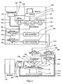
- FIG. 1 is a schematic representation of a test system according to a preferred embodiment of the present invention Invention.
- a wafer 10 is held by a wafer carrier or chuck 12 of a prober 14 by means of negative pressure, electrostatically or by means of an adhesive layer and positioned in all three spatial directions.
- Each pressure sensor comprises a pressure-sensitive section, a mechanical-electrical converter and a signal output.
- the mechanical electric transducer is a piezoelectric-effect solid, for example, a piezoelectric crystal having a surface constituting the pressure-sensitive portion of the pressure sensor.
- the mechanical-electrical transducer is a capacitor whose one capacitor plate is a pressure-deformable membrane whose surface is the pressure-sensitive portion of the pressure sensor.
- the signal output of the pressure sensor has a plurality of contact surfaces or pads, via which, if necessary, the pressure sensor, an electrical power, an electrical voltage or other electrical signal can be supplied, and via which a signal generated or influenced by the pressure sensor can be tapped.
- each pressure sensor may comprise an integrated circuit for generating, processing or converting electrical signals connected between the mechanical-electrical converter and the contact surfaces.
- the integrated circuit preferably has a comparator-based oscillator.
- the capacitor comprising the membrane is charged by a predetermined current, wherein the comparator compares the voltage across the capacitor with a reference voltage. As soon as the voltage across the capacitor reaches the reference voltage, the charging process switches over to a discharging process. This discharging process is either aborted controlled by a second comparator when falling below a second reference voltage, or it is completely discharged via a short circuit.
- Charging and discharging are repeated cyclically, producing a sequence of zeros and ones.
- the period ⁇ t of the charge / discharge cycle, or the sequence of zeros and ones, due to the pressure dependency of the capacitance of the capacitor is a function of the pressure.
- the integrated circuit may also generate an analog output signal.
- the pressure sensor may further comprise a transducer which converts the pressure-affected resonant frequency of the oscillator into an analog or digital signal.
- the integrated circuit is preferably provided for amplification, impedance conversion or digitization of the output signal of the piezoelectric sensor.
- the integrated circuit further comprises an analog or digital memory for storing one or more calibration coefficients with the aid of which it generates a calibrated output signal of the pressure sensor.
- a probe card 30 Opposite the surface 20 of the wafer 10 is a probe card 30 having a plurality of needles.
- the lateral arrangement of the needles or the needle tips corresponds to the lateral arrangement of the contact surfaces of a Pressure sensor.
- the needles of the probe card 30 contact the contact surfaces of one of the pressure sensors of the wafer 10, so that via the needles supplied to the pressure sensor, an electrical power or an electrical signal and a generated by the pressure sensor or affected electrical signal can be tapped.
- the probe card 30 has an opening 32, under which the tips of the needles, not shown, are arranged. Above the opening 32, a lid 34 is arranged, which is pressure-tightly connected to the probe card 30. Between the probe card 30 and the surface 20 of the wafer 10, a sealing lip 36 is arranged, which surrounds the opening 32 and the needles or their tips, for example in the form of a circle or a rectangle in a lateral direction.
- the sealing lip 36 forms a pressure-tight connection of the probe card 30 with the surface 20 of the wafer 10 so that a pressure-sealed against the environment cavity 38 between the lid 34, the probe card 30, the sealing lip 36 and the surface 20 of the wafer 10 is formed.
- the pressure-sensitive portion of the pressure sensor is arranged in this cavity 38.
- FIG. 2 displays an enlargement of a section Fig. 1 in which the cavity 38 is shown in cross-section, which is formed when, by a corresponding relative spatial arrangement of the probe card 30 and the wafer 10 and its surface 20 needles 40 of the probe card 30 on unillustrated contact surfaces of the pressure sensor on the surface 20 of the wafer 10 and contact them.
- the sealing lip 36 for example, a soft silicone lip, arranged, the outer edge 48, for example, by a bond, with the bottom 44 of the probe card 30 is pressure-tight manner.
- the sealing lip 36 has approximately the shape of a lateral surface of a blunt flat cone or a blunt flat pyramid. Near its inner edge 50, the sealing lip 36 has a peripheral, directed to the surface 20 of the wafer 10 edge 52 which rests on the surface 20 and forms a pressure-tight connection with this.
- the lid 34 On an upper side 56 of the probe card 30, the lid 34 is arranged and, for example by means of a bond, connected to the probe card 30, so that it closes the opening 32 of the probe card 30 pressure-tight.
- a bore or a venting channel 60 connects the miniature pressure chamber or the cavity 38 between the lid 34, the probe card 30, the sealing lip 36 and the surface 20 of the wafer 10 with a below with reference to Fig. 1 illustrated pressure system for setting a predetermined pressure in the cavity 38th
- FIG. 2 how out Fig. 2 can be seen, construction and preparation of the sealing lip 36 are simplified for geometric reasons when the needles 40 have the largest possible angle to the bottom 44 of the probe card 30.
- a preferred value of the angle between the needles 40 and the bottom 44 of the probe card 30 at which the present invention has been successfully tested is 10 degrees.
- FIG. 12 is a schematic plan view of a plurality of pressure sensors on a surface 20 of a wafer 10, in the manufacture of which the present invention can be used.
- Fig. 3A are as in the following Fig. 3B . 4A and 4B given some typical dimensions, which are given only by way of example.
- the individual pressure sensors 54 have a length of 2.12 mm and a width of 2.11 mm and are arranged in an approximately square grid with a mutual distance of 0.2 mm at the surface 20 of the wafer 10.
- Each pressure sensor 54 has a pressure sensitive section, electrical contact pads, and preferably an integrated circuit.
- Fig. 3B is a schematic representation of the sealing lip 36 in a section perpendicular to the surface 20 of the wafer 10.
- the sealing lip 36 is provided for 64 of in Fig. 3A
- the outer edge 48 of the sealing lip 36 laterally preferably has the shape of a circle with a diameter of 30 mm
- the inner edge 50 of the sealing lip 36 laterally preferably has the shape of a circle with a diameter of 15 mm.
- the sealing lip 36 has an edge 52 which laterally approximately has the shape of a square with side lengths of 18.48 mm and 18.56 mm and thus, as described above, encloses exactly 64 pressure sensors.
- the edge 52 projects vertically over the inner edge 50 by 0.5 mm.
- the angle by which the sealing lip 36 deviates from a plane is 10 °.
- FIGS. 4A and 4B show in a schematic plan view and a schematic sectional view of the lid 34th Fig. 4B shows a section perpendicular to the surface 20 of the wafer 10.
- the lid 34 is substantially axisymmetric. Its outer diameter is 60 mm.
- the lid 34 has a nose or a projection 66, which projects into the opening 32 of the probe card 30. This projection 66 reduces the volume of the cavity 38, thereby accelerating the setting of a predetermined pressure in the cavity 38.
- the cover 34 has the shape of a circular disc with two plane-parallel surfaces, a thickness of 10 mm and a circular 5 mm deep recess 68 opposite to the projection 66 on.
- the cover 34 also has the bore or the venting channel 60, via which a pressure equalization between the cavity 38 and the below with reference to Fig. 1 described printing system.
- the venting channel 60 ends in the region of the projection 66.
- the lid 34 has mounting holes 72 near its outer periphery 70 with or without a cut thread for mechanical attachment of the lid 34 to a particular mechanical stabilization device.
- This device for mechanical stabilization is required because otherwise already a slight negative or positive pressure in the cavity 38 causes a deformation or deflection of the probe card, which usually consists of a FR4 board.
- a negative pressure causes a reduction in the distance between the probe card and wafer. This reduction in pitch causes the tips of the needles on the surface 20 of the wafer 10 to be displaced so far that they leave the contact surfaces and damage the surrounding areas of the chip surface.
- This needle card 30 and cover 34 are mechanically stabilized by the mentioned, not shown in the figures device.
- the cover 34 is preferably made of a transparent material, for example Plexiglas or acrylic glass or PMMA (polymethyl methacrylate). For adjustment purposes, it is possible by means of a microscope or a camera attachment to be considered by the cover 34 to be tested IC or pressure sensor.
- a transparent material for example Plexiglas or acrylic glass or PMMA (polymethyl methacrylate).
- a pressure delivery system 100 provides two different predetermined pressures p1, p2 via pressure vessels 102, 104, which may be alternately applied to the cavity 38 via devices described below.
- a control PC running control software is connected to a pressure calibrator 120 via a data bus 112, such as a GPIP bus.
- the pressure calibrator 120 is connected to a reference vacuum pump 126 and a vacuum pump 128 via vacuum lines 122, 124. Controlled by the control PC 110, the pressure calibrator 120 alternately generates the two pressures p1, p2 to be applied to the cavity 38 and thus to the pressure sensitive portion of the pressure sensor to be tested or calibrated.
- the control PC 110 is further connected to a voltage source 134 for generating two voltages via a data bus 132, which in turn is preferably a GPIP bus. These two voltages are applied via control lines 142, 144 to solenoid control valves Va 152 and Vb 154 to open and close them.
- the magnetic control valves Va 152 and Vb 154 are connected to the pressure calibrator 120 via a forked vacuum line 156 on the pressure input side.
- the magnetic control valve Va 152 are connected via a vacuum line 162 to the first pressure vessel 102 and the solenoid control valve Vb 154 connected via a vacuum line 164 to the second pressure vessel 104.
- the pressure delivery system 100 is independent of what is described below other components of the pressure system in the pressure vessels 102, 104 two predetermined pressures p1, p2 ready.
- the control PC or the control program running on it via the data buses 112, 132 and the voltage source 134 control the pressure calibrator 120 and the magnetic control valves Va 152 and Vb 154.
- the pressure calibrator 120 generates the first predetermined to be provided in the first pressure vessel 102 Pressure p1, wherein at the same time by an open solenoid control valve Va 152 and a closed solenoid control valve Vb 154 only the first pressure vessel 102 is connected to the pressure calibrator 120, and to be provided in the second pressure vessel 104 second predetermined pressure p2, via a closed magnet Control valve Va 152 and an open solenoid control valve Vb 154 only the second pressure vessel 104 is connected to the pressure calibrator 120.
- the pressure vessels 102, 104 are each connected to a magnetic control valve V1 182 or V2 184.
- the solenoid control valves V1 182 and V2 184 are further connected in parallel to a solenoid control valve V3 190 via a multi-forked vacuum line 188 with a pressure cell 194 and the vent passage 60 to the cavity 38.
- the solenoid control valve V3 190 is further connected to the surrounding atmosphere.
- the solenoid control valves V1 182, V2 184 and V3 190 are in Fig. 1 shown as 3-way valves, which are used only as 2-way valves, and whose third inlet / outlet is always closed.
- the reason for using 3-way valves as 2-way valves is the low selection of pneumatic valves suitable for use in the vacuum range.
- a mainframe or large computer 200 which controls the testing and / or calibration of the pressure sensors, is connected to a test head or a test head 204 via an interface 202, preferably a TH-MF interface.
- the Test head 204 receives a pressure measurement signal from the pressure cell 194 via a control line 210 and sends control signals for the magnetic control valves V1 182, V2 184 and V3 190 via control lines 212, 214, 216.
- a test program running on the mainframe computer 200 can thus be transmitted via the test head 204 and by means of the solenoid control valves V1 182, V2 184 and V3 190 control the pressure applied in the cavity 38 and thus the pressure-sensitive portion of the pressure sensor to be tested or calibrated.
- valves V1 182 and V2 184 are closed, and the valve V3 190 is open.
- the system in particular the cavity 38, is ventilated and the ambient pressure p3 is applied.
- the solenoid control valves V3 190 and V2 184 are closed and the solenoid control valve V1 182 opened, there is fluid communication between the first pressure vessel 102 and the cavity 38.
- the cavity 38 is provided in the first pressure vessel first predetermined pressure p1 one. If the solenoid control valves V3 190 and V1 182 are closed and the solenoid control valve V2 184 is opened, there is fluid communication between the second pressure vessel 104 and the cavity 38.
- the second predetermined provided in the second pressure vessel 104 Pressure p2 on.
- a test program routine is started.
- the test program routine tests the pressure sensor and the integrated circuit and reads out the pressure analog sensor data or the digital or analog output signals of the pressure sensor representative of the pressure sensed by the pressure sensor.
- the calibration of the pressure sensor preferably takes place, as provided by the pressure system described above, at at least two different temperatures T1, T2 and at at least three different pressures p1, p2, p3 per set temperature T1, T2. From the measured data thus obtained, individual calibration coefficients are then calculated for the pressure sensor to be calibrated and, if provided for the pressure sensor, stored in an integrated memory of the pressure sensor. If the pressure sensor is merely tested, it is checked whether the deviations of the measured values determined by the pressure sensor from the respectively actual applied pressures p1, p2, p3 are within permissible limits or if determined calibration coefficients are within a predetermined range. Pressure sensors that do not meet these conditions are not packaged after a subsequent separation but discarded.
- a calibration routine is started in each case immediately after detection of the pressure measurement signals of a pressure sensor by the test program.
- the calibration routine determines from the measurement data for the first predetermined temperature T1 stored in the file and the measurement data for the second predetermined temperature T2 individual calibration coefficients for the respective pressure sensor and puts these optionally in a space provided for the calibration coefficients memory of the integrated circuit of the pressure sensor from.
- the calibration may be due to measurements at one or more than two temperatures and at one, two or four or more Press done.
- the probe card 30 can each contact only a single pressure sensor or at the same time a plurality of pressure sensors. If the sealing lip 36 also encloses this plurality of simultaneously contacted pressure sensors, so that the predetermined pressure p1, p2 or the ambient pressure p3 simultaneously applied to all contacted pressure sensors or their pressure-sensitive sections, all contacted pressure sensors can be calibrated simultaneously.
- the wafer 10 is somewhat moved away from the probe card 30 after measuring, testing or calibrating a group of pressure sensors so that the needles 40 are no longer open the contact surfaces of the pressure sensors rest and the edge 52 of the sealing lip 36 no longer rests on the surface 20 of the wafer 10.
- the wafer 10 is then moved in the lateral direction by a distance which corresponds to the grid dimension, with which the pressure sensors are arranged on the surface 20 of the wafer 10, or a multiple thereof.
- the wafer 10 with the wafer carrier 12 is moved back to the probe card 30, so that the needles 40 contact the contact surfaces of the pressure sensors on the surface 20 of the wafer 10 and the edge 52 of the sealing lip 36 completely rests against the surface 20 of the wafer 10. Subsequently, one or more Measured, tested or calibrated pressure sensors that have not yet been measured, tested or calibrated.
- the above-described pressure-providing system 100 is provided for generating pressures that are lower than the ambient pressure.
- the present invention can also be used for pressure sensors or their calibration in the overpressure region, wherein only the pressure calibrator could be provided with a corresponding pressure by a compressor or an overpressure pump, a compressed gas cylinder or the like.
- an extension of the pressure delivery system 100 is readily possible to more than two pressures that differ from the ambient pressure possible.
- respective pumps 126, 128, valves 152, 154, 182, 184, 190, pressure vessels 102, 104, fluid conduits 112, 132, 156, 162, 164, 172 are provided , 174, 188, 192, a corresponding pressure cell 194 and a corresponding pressure calibrator 120 are used.
- the pressure cell 194 is either as in Fig. 1 represented via a fork-shaped vacuum line 192 with the solenoid control valve V3 190 and the cavity 38 or via a separate vacuum line directly connected to the cavity 38 or arranged in this, as already described with reference to FIG Fig. 4 was explained.
- the pressure sensor comprises a pressure-sensitive portion on the surface 20 of the wafer 10, which is disposed between the contact surfaces contacted by the contact pins 40.
- the pressure-sensitive portion of each pressure sensor can also be arranged next to the contact surfaces.
- the contact needles 40 of the probe card 30 be arranged outside the sealing lip 36.
- the pressure sensor may have an optical signal output and / or an optical power input. In this case, in addition to a (smaller) number of needles 40 or instead of the needles 40, an optical interface is required to test the pressure sensors on the surface 20 of the wafer 10.
Claims (19)
- Procédé pour tester ou étalonner un capteur de pression parmi une pluralité de capteurs de pression réalisés dans une tranche de silicium (10), le capteur de pression présentant un segment sensible à la pression et une sortie de signal, la sortie de signal comportant des faces de contact, et les faces de contact et le segment sensible à la pression étant disposés sur une surface de la tranche de silicium (10), aux étapes suivantes consistant à:préparer une carte à aiguilles (30) qui présente des aiguilles (40) avec des pointes d'aiguille, la carte à aiguilles (30) présentant une face supérieure et une face inférieure, la face inférieure de la carte à aiguilles étant orientée vers la surface de la tranche de silicium, les aiguilles (40) étant disposées sur la face inférieure de la carte à aiguilles, et sur la face inférieure de la carte à aiguilles étant par ailleurs placée une lèvre d'étanchéité (36) qui entoure les pointes d'aiguille;assembler de manière étanche à la pression le segment sensible à la pression du capteur de pression avec un conduit à fluide (60; 192) en plaçant la lèvre d'étanchéité sur la surface de la tranche de silicium, les pointes d'aiguille étant par ailleurs amenées en contact électrique avec les faces de contact;appliquer une pression prédéterminée (p1, p2, p3) sur le conduit à fluide (60; 192) au segment sensible à la pression du capteur de pression; etrecevoir un signal de la sortie de signal du capteur de pression par les aiguilles de la carte à aiguilles.
- Procédé selon la revendication 1, dans lequel l'étape consistant à appliquer la pression prédéterminée (p1, p2, p3) est réalisée avant une étape consistant à individualiser la tranche de silicium (10).
- Procédé selon la revendication 1 ou 2, comprenant par ailleurs une étape consistant à fixer la tranche de silicium (10) à un porte-tranche de silicium (12).
- Procédé selon l'une des revendications 1 à 3, comprenant par ailleurs une étape consistant à prélever la tranche de silicium (10) d'une claie.
- Procédé selon l'une des revendications 1 à 4, comprenant par ailleurs les étapes suivantes consistant à:déterminer un paramètre d'étalonnage à partir de la pression déterminée (p1, p2, p3) et du signal reçu de la sortie de signal du capteur de pression; etmémoriser le paramètre d'étalonnage dans un moyen de mémoire du capteur de pression.
- Procédé selon l'une des revendications 1 à 5, comprenant par ailleurs une étape consistant à déterminer si le capteur de pression est fonctionnel, en fonction du signal reçu de la sortie de signal du capteur de pression.
- Procédé selon l'une des revendications 1 à 6, comprenant par ailleurs les étapes suivantes consistant à:individualiser le segment sensible à la pression du capteur de pression du conduit à fluide (60; 192);déplacer la tranche de silicium (10) et le conduit à fluide (60; 192) l'un par rapport à l'autre d'un trajet prédéterminé parallèle à la tranche de silicium (10);assembler de manière étanche à la pression un segment sensible à la pression d'un autre capteur de pression de la pluralité de capteurs de pression réalisés dans la tranche de silicium avec le conduit à fluide (60; 192);appliquer la pression prédéterminée (p1, p2, p3) sur le conduit à fluide (60; 192) au segment sensible à la pression de l'autre capteur de pression; etrecevoir un autre signal d'une sortie de signal de l'autre capteur de pression.
- Procédé selon l'une des revendications 1 à 7, comprenant par ailleurs les étapes suivantes consistant à:régler une température du capteur de pression à une première valeur (T1) avant la réception du signal;régler la température du capteur de pression à une deuxième valeur (T2) après la réception du signal;appliquer la pression prédéterminée (p1, p2, p3) sur le conduit à fluide (60; 192) au segment sensible à la pression du capteur de pression après le réglage de la température du capteur de pression à la deuxième valeur (T2); etrecevoir un autre signal de la sortie de signal du capteur de pression.
- Procédé selon la revendication 8, dans lequel les étapes consistant à régler la température comportent, chacune, une étape consistant à régler une température d'un porte-tranche de silicium.
- Procédé selon l'une des revendications 1 à 9, comprenant par ailleurs une étape consistant à mettre en contact la sortie de signal du capteur de pression avec une carte à aiguilles (30).
- Procédé selon la revendication 1, dans lequel les aiguilles s'étendent à partir de la carte à aiguilles de sorte que les aiguilles forment avec la face inférieure de la carte à aiguilles un angle aigu.
- Procédé pour fabriquer un élément de capteur de pression, aux étapes suivantes consistant à:préparer une tranche de silicium (10) avec une pluralité de capteurs de pression, chaque capteur de pression présentant un segment sensible à la pression et une sortie de signal;appliquer un procédé selon l'une des revendications 1 à 11 sur l'un de la pluralité de capteurs de pression;individualiser la tranche de silicium après l'application du procédé selon l'une des revendications 1 à 11, pour obtenir le capteur de pression individualisé; etmettre sous boîtier le capteur de pression individualisé, pour obtenir l'élément de capteur de pression.
- Procédé selon la revendication 12 avec renvoi à la revendication 6, dans lequel l'étape consistant à mettre sous boîtier n'est réalisée que si le capteur de pression est fonctionnel.
- Dispositif pour appliquer une pression prédéterminée sur un capteur de pression d'une pluralité de capteurs de pression réalisés dans une tranche de silicium et pour recevoir un signal d'une sortie de signal, présentant des faces de contact, du capteur de pression, le capteur de pression présentant un segment sensible à la pression, et les faces de contact et le segment sensible à la pression étant disposés sur une surface de la tranche de silicium, aux caractéristiques suivantes:un moyen destiné à préparer une carte à aiguilles (30) qui présente des aiguilles (40) avec des pointes d'aiguille, la carte à aiguilles (30) présentant une face supérieure et une face inférieure, la face inférieure de la carte à aiguilles étant orientée vers la surface de la tranche de silicium, les aiguilles (40) étant disposées sur la face inférieure de la carte à aiguilles, et sur la face inférieure de la carte à aiguilles étant par ailleurs placée une lèvre d'étanchéité (36) qui entoure les pointes d'aiguille;un moyen (36) destiné à assembler de manière étanche à la pression le segment sensible à la pression avec un conduit à fluide (60; 192) qui est prévu pour alimenter la pression prédéterminée (p1, p2, p3) en plaçant la lèvre d'étanchéité sur la surface de la tranche de silicium, les pointes d'aiguille étant par ailleurs amenées en contact électrique avec les faces de contact;un moyen (30, 40) destiné à recevoir le signal de la sortie de signal du capteur de pression par les aiguilles de la carte à aiguilles.
- Dispositif selon la revendication 14, dans lequel le moyen destiné à recevoir est un testeur de tranche de silicium.
- Dispositif selon la revendication 14, dans lequel la lèvre d'étanchéité (36) entoure par ailleurs les aiguilles (40) de la carte à aiguilles (30).
- Dispositif selon la revendication 18, dans lequel la carte à aiguilles (30) présente par ailleurs un couvercle (34) qui obture de manière étanche à la pression une ouverture de la carte à aiguilles (30) à la face supérieure (56) de la carte à aiguilles.
- Dispositif selon la revendication 17, dans lequel le couvercle (34) présente un matériau transparent.
- Carte à aiguilles pour tester ou étalonner un capteur de pression parmi une pluralité de capteurs de pression réalisés dans une tranche de silicium (10), le capteur de pression présentant un segment sensible à la pression et une sortie de signal, la sortie de signal comportant des faces de contact, et les faces de contact et le segment sensible à la pression étant disposés sur une surface de la tranche de silicium (10), aux caractéristiques suivantes:un corps de carte à aiguilles avec une face supérieure et une face inférieure, la face inférieure de la carte à aiguilles devant être orientée vers la surface de la tranche de silicium lorsque le capteur de pression est testé ou étalonné;des aiguilles (40) avec des pointes d'aiguille qui sont disposées à la face inférieure de la carte à aiguilles, etune lèvre d'étanchéité (36) qui est placée sur la face inférieure de la carte à aiguilles de sorte qu'elle entoure les pointes d'aiguille.
Applications Claiming Priority (3)
| Application Number | Priority Date | Filing Date | Title |
|---|---|---|---|
| DE10128235 | 2001-06-11 | ||
| DE10128235 | 2001-06-11 | ||
| PCT/EP2002/006350 WO2002101348A1 (fr) | 2001-06-11 | 2002-06-10 | Procede et dispositif pour essayer ou etalonner un capteur de pression forme dans une tranche de silicium |
Publications (2)
| Publication Number | Publication Date |
|---|---|
| EP1397656A1 EP1397656A1 (fr) | 2004-03-17 |
| EP1397656B1 true EP1397656B1 (fr) | 2009-05-06 |
Family
ID=7687880
Family Applications (1)
| Application Number | Title | Priority Date | Filing Date |
|---|---|---|---|
| EP02730292A Expired - Fee Related EP1397656B1 (fr) | 2001-06-11 | 2002-06-10 | Procede et dispositif pour essayer ou etalonner un capteur de pression forme dans une tranche de silicium |
Country Status (3)
| Country | Link |
|---|---|
| EP (1) | EP1397656B1 (fr) |
| DE (1) | DE50213526D1 (fr) |
| WO (1) | WO2002101348A1 (fr) |
Families Citing this family (7)
| Publication number | Priority date | Publication date | Assignee | Title |
|---|---|---|---|---|
| WO2006128475A1 (fr) * | 2005-05-27 | 2006-12-07 | Fraunhofer-Gesellschaft zur Förderung der angewandten Forschung e.V. | Procede et dispositif d'essai ou d'etalonnage d'un capteur de pression enferme dans un boitier |
| DE102005045079B4 (de) * | 2005-09-21 | 2010-02-25 | Infineon Technologies Ag | Konzept zum Testen eines Drucksensors und eine Düse |
| JP4246197B2 (ja) * | 2005-12-08 | 2009-04-02 | 三菱電機株式会社 | センサチップの破壊強度検査方法 |
| EP2259027B1 (fr) | 2009-06-04 | 2012-12-05 | Sensirion AG | Procédé et appareil de traitement de dispositifs de capteurs individuels |
| EP2418503B1 (fr) | 2010-07-14 | 2013-07-03 | Sensirion AG | Tête d'aiguille |
| AT511058B1 (de) * | 2011-03-17 | 2012-09-15 | Rainer Dr Gaggl | Verfahren und vorrichtung zum prüfen von drucksensoren |
| IT201800006903A1 (it) * | 2018-07-04 | 2020-01-04 | Scheda di misura per applicazioni ad alta frequenza |
Family Cites Families (7)
| Publication number | Priority date | Publication date | Assignee | Title |
|---|---|---|---|---|
| US4567432A (en) * | 1983-06-09 | 1986-01-28 | Texas Instruments Incorporated | Apparatus for testing integrated circuits |
| US4777716A (en) * | 1986-08-25 | 1988-10-18 | Motorola Inc. | Method for low pressure testing of a solid state pressure sensor |
| EP0265816B1 (fr) * | 1986-10-28 | 1991-08-28 | Sumitomo Electric Industries Limited | Méthode de mesure d'un capteur de pression à semi-conducteur |
| JPH01216550A (ja) * | 1988-02-25 | 1989-08-30 | Nec Corp | 半導体ウェハープローバー用温度制御ステージ |
| US5421956A (en) * | 1991-11-20 | 1995-06-06 | Nippondenso Co., Ltd. | Method of fabricating an integrated pressure sensor |
| US6373271B1 (en) * | 1999-12-29 | 2002-04-16 | Motorola, Inc. | Semiconductor wafer front side pressure testing system and method therefor |
| DE10000133C2 (de) * | 2000-01-04 | 2003-06-26 | Karl Suss Dresden Gmbh | Prober für Drucksensoren |
-
2002
- 2002-06-10 EP EP02730292A patent/EP1397656B1/fr not_active Expired - Fee Related
- 2002-06-10 WO PCT/EP2002/006350 patent/WO2002101348A1/fr active Application Filing
- 2002-06-10 DE DE50213526T patent/DE50213526D1/de not_active Expired - Lifetime
Also Published As
| Publication number | Publication date |
|---|---|
| DE50213526D1 (de) | 2009-06-18 |
| WO2002101348A1 (fr) | 2002-12-19 |
| EP1397656A1 (fr) | 2004-03-17 |
Similar Documents
| Publication | Publication Date | Title |
|---|---|---|
| EP2932221B1 (fr) | Procédé de test d'étanchéité d'un boîtier | |
| DE10000133C2 (de) | Prober für Drucksensoren | |
| DE102017220132A1 (de) | Verfahren und Vorrichtung zur Korrektur von Drucksensoren | |
| DE112006002853T5 (de) | Prüfvorrichtung, Stiftelektronikkarte, elektrische Vorrichtung und Schalter | |
| EP1397656B1 (fr) | Procede et dispositif pour essayer ou etalonner un capteur de pression forme dans une tranche de silicium | |
| DE102010031452A1 (de) | Niederdrucksensor-Vorrichtung mit hoher Genauigkeit und hoher Empfindlichkeit | |
| DE10018404A1 (de) | Halbleiterdehnungssensor | |
| DE4122435A1 (de) | Verfahren zur herstellung von beschleunigungssensoren und beschleunigungssensor | |
| DE102007062713A1 (de) | Drucksensor und Verfahren zu dessen Kalibrierung | |
| EP2668483A1 (fr) | Composant microélectromécanique et procédé pour tester un composant microélectromécanique | |
| DE3436440A1 (de) | Halbleiter-messeinrichtung | |
| DE10339939A1 (de) | Intergierte Schalltungsanordnung und Verfahren zur Herstellung derselben | |
| WO2020084043A1 (fr) | Structure de mesure d'extensibilité comprenant un support structuré | |
| US20050116729A1 (en) | Method and device for testing or calibrating a pressure sensor on a wafer | |
| DE102006004247B4 (de) | Konzept zum Testen einer integrierten Schaltungsanordnung | |
| DE19601078A1 (de) | Druckkraftsensor | |
| DE102008054428A1 (de) | Aufbau eines Drucksensors | |
| WO2006128475A1 (fr) | Procede et dispositif d'essai ou d'etalonnage d'un capteur de pression enferme dans un boitier | |
| EP3566037B1 (fr) | Capteur micromécanique linéarisé | |
| DE102017212422A1 (de) | Drucksensoranordnung und Verfahren zu deren Herstellung | |
| DE102017212866A1 (de) | Drucksensoranordnung, Messvorrichtung und Verfahren zu deren Herstellung | |
| DE102007016553A1 (de) | Vorrichtung und Verfahren zur elektrischen Kontaktierung von Halbleiter-Bauelementen auf einem Wafer | |
| DE102017212838A1 (de) | Drucksensoranordnung, Messvorrichtung und Verfahren zu deren Herstellung | |
| DE102007057694B4 (de) | Leckageerkennung bei einem Gehäuse eines elektronischen Steuergeräts | |
| WO2009121426A2 (fr) | Capteur périphérique et procédé de fabrication d'un capteur périphérique par insertion et par assemblage à force/par coopération de formes |
Legal Events
| Date | Code | Title | Description |
|---|---|---|---|
| PUAI | Public reference made under article 153(3) epc to a published international application that has entered the european phase |
Free format text: ORIGINAL CODE: 0009012 |
|
| AK | Designated contracting states |
Kind code of ref document: A1 Designated state(s): AT BE CH CY DE DK ES FI FR GB GR IE IT LI LU MC NL PT SE TR |
|
| AX | Request for extension of the european patent |
Extension state: AL LT LV MK RO SI |
|
| 17P | Request for examination filed |
Effective date: 20040305 |
|
| RIN1 | Information on inventor provided before grant (corrected) |
Inventor name: KOESTER, OLIVER Inventor name: SLOTKOWSKI, JOHANN |
|
| RBV | Designated contracting states (corrected) |
Designated state(s): DE FR GB |
|
| R17P | Request for examination filed (corrected) |
Effective date: 20040305 |
|
| GRAP | Despatch of communication of intention to grant a patent |
Free format text: ORIGINAL CODE: EPIDOSNIGR1 |
|
| GRAS | Grant fee paid |
Free format text: ORIGINAL CODE: EPIDOSNIGR3 |
|
| GRAA | (expected) grant |
Free format text: ORIGINAL CODE: 0009210 |
|
| AK | Designated contracting states |
Kind code of ref document: B1 Designated state(s): DE FR GB |
|
| REG | Reference to a national code |
Ref country code: GB Ref legal event code: FG4D Free format text: NOT ENGLISH |
|
| REF | Corresponds to: |
Ref document number: 50213526 Country of ref document: DE Date of ref document: 20090618 Kind code of ref document: P |
|
| PLBE | No opposition filed within time limit |
Free format text: ORIGINAL CODE: 0009261 |
|
| STAA | Information on the status of an ep patent application or granted ep patent |
Free format text: STATUS: NO OPPOSITION FILED WITHIN TIME LIMIT |
|
| REG | Reference to a national code |
Ref country code: FR Ref legal event code: ST Effective date: 20100226 |
|
| 26N | No opposition filed |
Effective date: 20100209 |
|
| GBPC | Gb: european patent ceased through non-payment of renewal fee |
Effective date: 20090806 |
|
| PG25 | Lapsed in a contracting state [announced via postgrant information from national office to epo] |
Ref country code: FR Free format text: LAPSE BECAUSE OF NON-PAYMENT OF DUE FEES Effective date: 20090706 |
|
| PG25 | Lapsed in a contracting state [announced via postgrant information from national office to epo] |
Ref country code: GB Free format text: LAPSE BECAUSE OF NON-PAYMENT OF DUE FEES Effective date: 20090806 |
|
| PGFP | Annual fee paid to national office [announced via postgrant information from national office to epo] |
Ref country code: DE Payment date: 20110826 Year of fee payment: 10 |
|
| REG | Reference to a national code |
Ref country code: DE Ref legal event code: R119 Ref document number: 50213526 Country of ref document: DE Effective date: 20130101 |
|
| PG25 | Lapsed in a contracting state [announced via postgrant information from national office to epo] |
Ref country code: DE Free format text: LAPSE BECAUSE OF NON-PAYMENT OF DUE FEES Effective date: 20130101 |