EP1397656B1 - Method and device for testing or calibrating a pressure sensor on a wafer - Google Patents
Method and device for testing or calibrating a pressure sensor on a wafer Download PDFInfo
- Publication number
- EP1397656B1 EP1397656B1 EP02730292A EP02730292A EP1397656B1 EP 1397656 B1 EP1397656 B1 EP 1397656B1 EP 02730292 A EP02730292 A EP 02730292A EP 02730292 A EP02730292 A EP 02730292A EP 1397656 B1 EP1397656 B1 EP 1397656B1
- Authority
- EP
- European Patent Office
- Prior art keywords
- pressure
- pressure sensor
- wafer
- probe card
- sensitive portion
- Prior art date
- Legal status (The legal status is an assumption and is not a legal conclusion. Google has not performed a legal analysis and makes no representation as to the accuracy of the status listed.)
- Expired - Lifetime
Links
Images


Classifications
-
- G—PHYSICS
- G01—MEASURING; TESTING
- G01L—MEASURING FORCE, STRESS, TORQUE, WORK, MECHANICAL POWER, MECHANICAL EFFICIENCY, OR FLUID PRESSURE
- G01L27/00—Testing or calibrating of apparatus for measuring fluid pressure
- G01L27/002—Calibrating, i.e. establishing true relation between transducer output value and value to be measured, zeroing, linearising or span error determination
- G01L27/005—Apparatus for calibrating pressure sensors
Definitions
- the present invention relates to a method and apparatus for testing or calibrating a pressure sensor on a wafer.
- Microelectronic circuits formed in or on a wafer are usually tested prior to wafer singulation and packaging of the individual circuits. These tests are performed by automatic wafer probers or wafer testers.
- a Waferprober includes a handling system or a handling device, which takes a single wafer from a storage unit (Horde) and passes the actual Prober. The wafer is placed on a movable carrier plate, the so-called chuck and locked there by suction or electrostatically or by means of an adhesive layer.
- the prober makes an exact positioning of the wafer to be tested in all three spatial directions. After the successful positioning of the wafer to be tested, precisely one integrated circuit of the wafer always comes to lie below a immovably mounted probe card or probe card.
- the probe card has a plurality of tungsten needles whose arrangement corresponds exactly to the geometry of the microscopic pads or contact points on the integrated circuit.
- the chuck is moved in the height or in the direction perpendicular to the wafer plane z-direction until the needles of the probe card put on the pads and so make electrically conductive connections to the same.
- About macroscopic taps, which are associated with the needles of the probe card and electrically connected thereto, electrical signals are passed to the integrated circuit or tapped from the integrated circuit generated electrical signals.
- a probe card can contact one or more integrated circuits at a time.
- the wafer is repeatedly moved with the chuck by predetermined distances parallel to the wafer plane and moved up to the needles of the probe card. Since the exact positions of all integrated circuits on a wafer are known, a one-time positioning of the wafer suffices.
- the wafer prober is connected via a serial interface to a computer or a workstation of a test system, so that a test program executed by the test system or the computer can communicate with the wafer prober.
- the integrated circuit comprises a pressure sensor
- only a test of electrical functions and functionalities of the integrated formwork is possible by means of the above-described Waferprobers.
- the wafer is singulated and electrically functioning integrated circuits are packaged, i. H. inserted or cast in housing. Subsequently, a test and possibly a calibration of the isolated and packaged pressure sensors.
- the housing may need to have one or more additional contacts which are used only once, namely when calibrating the pressure sensor, but which increase the production costs and increase the risk during the entire life of the pressure sensor Increase damage or destruction of the same.
- the document US-A-4,777,716 Discloses a method and apparatus for testing a wafer equipped with pressure sensors.
- a plate is connected to a vacuum housing from which electrical contact pins protrude. By applying this plate to the wafer surrounded by a sealing lip, individual pressure sensors of this wafer can be contacted and checked.
- the object of the present invention is to provide an improved test or calibration method for a pressure sensor, a manufacturing method for a pressure sensor and a device that simplify testing and calibration of a pressure sensor.
- the present invention is based on the idea of testing or calibrating pressure sensors, in particular surface micromechanical absolute pressure sensors, and, in particular, pressure sensors provided for a vacuum region, even in a wafer, ie before it is singulated.
- a pressure-sensitive portion of the pressure sensor is connected, for example by means of a sealing lip with a fluid line, via which one or more successively predetermined pressures can be applied to the pressure-sensitive portion of the pressure sensor.
- a signal generated by the pressure sensor in response to the pressure at a signal output is received.
- the test or calibration is preferably carried out by means of an automatic wafer tester with a probe card, wherein the sealing lip is arranged between the probe card and a surface of the wafer on which the pressure-sensitive portion of the pressure sensor is arranged.
- This sealing lip encloses the pressure-sensitive section, the needles of the probe card and pads of the pressure sensor lateral, for example, in the form of a circle or a rectangle and seals the gap between the surface of the wafer on the one hand and the probe card on the other hand, in which the pressure-sensitive portion of the pressure sensor is arranged, pressure-tight against the environment.
- a standard wafer tester is modified and in particular provided with the sealing lip under the probe card.
- An opening in the needle tips which is frequently present in conventional needle cards is optionally pressure-tightly closed by means of a lid, which preferably has a transparent material, for example PMMA (polymethyl methacrylate).
- a fluid conduit connects the thus completely pressure-tightly enclosed cavity between the surface of the wafer, the probe card and the lid with a pressure system which generates the predetermined pressure (s).
- An advantage of the present invention is that the pressure sensors can still be tested or calibrated on the non-isolated wafer. This can be done simultaneously with a test of the electrical properties of the integrated circuit or its functionality. A re-handling, positioning and contacting the isolated and packaged pressure sensors is not required. Defective pressure sensors are not housed because they are already identified. Corresponding to the resulting simplification and shortening of the manufacturing process in the area of testing and calibration, considerable cost advantages arise, which enable the use of integrated pressure sensors in many products only economically. Furthermore, the present invention enables the use of integrated pressure sensors in products in which a test or calibration after singulation for technical reasons is not feasible.
- the housed pressure sensor or its housing must also no contacts for the transmission of calibration coefficients in a integrated memory element (eg an EEPROM). Therefore, the size and cost of the housing can be reduced and the risk of later damage to these contacts avoided.
- a integrated memory element eg an EEPROM
- Another advantage of the present invention is its implementability by a modification of a conventional wafer tester. The present invention therefore produces only low investment costs.
- a preferred field of application of the present invention is the production of absolute pressure sensors, especially in the vacuum range between 0 and 1 bar and in particular of surface micromechanical absolute pressure sensors, in large quantities and in particular for applications in which the customer after installation of the absolute pressure sensor in his overall system no way to calibrate the sensor has more.
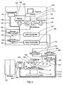
- FIG. 1 is a schematic representation of a test system according to a preferred embodiment of the present invention Invention.
- a wafer 10 is held by a wafer carrier or chuck 12 of a prober 14 by means of negative pressure, electrostatically or by means of an adhesive layer and positioned in all three spatial directions.
- Each pressure sensor comprises a pressure-sensitive section, a mechanical-electrical converter and a signal output.
- the mechanical electric transducer is a piezoelectric-effect solid, for example, a piezoelectric crystal having a surface constituting the pressure-sensitive portion of the pressure sensor.
- the mechanical-electrical transducer is a capacitor whose one capacitor plate is a pressure-deformable membrane whose surface is the pressure-sensitive portion of the pressure sensor.
- the signal output of the pressure sensor has a plurality of contact surfaces or pads, via which, if necessary, the pressure sensor, an electrical power, an electrical voltage or other electrical signal can be supplied, and via which a signal generated or influenced by the pressure sensor can be tapped.
- each pressure sensor may comprise an integrated circuit for generating, processing or converting electrical signals connected between the mechanical-electrical converter and the contact surfaces.
- the integrated circuit preferably has a comparator-based oscillator.
- the capacitor comprising the membrane is charged by a predetermined current, wherein the comparator compares the voltage across the capacitor with a reference voltage. As soon as the voltage across the capacitor reaches the reference voltage, the charging process switches over to a discharging process. This discharging process is either aborted controlled by a second comparator when falling below a second reference voltage, or it is completely discharged via a short circuit.
- Charging and discharging are repeated cyclically, producing a sequence of zeros and ones.
- the period ⁇ t of the charge / discharge cycle, or the sequence of zeros and ones, due to the pressure dependency of the capacitance of the capacitor is a function of the pressure.
- the integrated circuit may also generate an analog output signal.
- the pressure sensor may further comprise a transducer which converts the pressure-affected resonant frequency of the oscillator into an analog or digital signal.
- the integrated circuit is preferably provided for amplification, impedance conversion or digitization of the output signal of the piezoelectric sensor.
- the integrated circuit further comprises an analog or digital memory for storing one or more calibration coefficients with the aid of which it generates a calibrated output signal of the pressure sensor.
- a probe card 30 Opposite the surface 20 of the wafer 10 is a probe card 30 having a plurality of needles.
- the lateral arrangement of the needles or the needle tips corresponds to the lateral arrangement of the contact surfaces of a Pressure sensor.
- the needles of the probe card 30 contact the contact surfaces of one of the pressure sensors of the wafer 10, so that via the needles supplied to the pressure sensor, an electrical power or an electrical signal and a generated by the pressure sensor or affected electrical signal can be tapped.
- the probe card 30 has an opening 32, under which the tips of the needles, not shown, are arranged. Above the opening 32, a lid 34 is arranged, which is pressure-tightly connected to the probe card 30. Between the probe card 30 and the surface 20 of the wafer 10, a sealing lip 36 is arranged, which surrounds the opening 32 and the needles or their tips, for example in the form of a circle or a rectangle in a lateral direction.
- the sealing lip 36 forms a pressure-tight connection of the probe card 30 with the surface 20 of the wafer 10 so that a pressure-sealed against the environment cavity 38 between the lid 34, the probe card 30, the sealing lip 36 and the surface 20 of the wafer 10 is formed.
- the pressure-sensitive portion of the pressure sensor is arranged in this cavity 38.
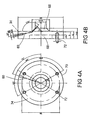
- FIG. 2 displays an enlargement of a section Fig. 1 in which the cavity 38 is shown in cross-section, which is formed when, by a corresponding relative spatial arrangement of the probe card 30 and the wafer 10 and its surface 20 needles 40 of the probe card 30 on unillustrated contact surfaces of the pressure sensor on the surface 20 of the wafer 10 and contact them.
- the sealing lip 36 for example, a soft silicone lip, arranged, the outer edge 48, for example, by a bond, with the bottom 44 of the probe card 30 is pressure-tight manner.
- the sealing lip 36 has approximately the shape of a lateral surface of a blunt flat cone or a blunt flat pyramid. Near its inner edge 50, the sealing lip 36 has a peripheral, directed to the surface 20 of the wafer 10 edge 52 which rests on the surface 20 and forms a pressure-tight connection with this.
- the lid 34 On an upper side 56 of the probe card 30, the lid 34 is arranged and, for example by means of a bond, connected to the probe card 30, so that it closes the opening 32 of the probe card 30 pressure-tight.
- a bore or a venting channel 60 connects the miniature pressure chamber or the cavity 38 between the lid 34, the probe card 30, the sealing lip 36 and the surface 20 of the wafer 10 with a below with reference to Fig. 1 illustrated pressure system for setting a predetermined pressure in the cavity 38th
- FIG. 2 how out Fig. 2 can be seen, construction and preparation of the sealing lip 36 are simplified for geometric reasons when the needles 40 have the largest possible angle to the bottom 44 of the probe card 30.
- a preferred value of the angle between the needles 40 and the bottom 44 of the probe card 30 at which the present invention has been successfully tested is 10 degrees.
- FIG. 12 is a schematic plan view of a plurality of pressure sensors on a surface 20 of a wafer 10, in the manufacture of which the present invention can be used.
- Fig. 3A are as in the following Fig. 3B . 4A and 4B given some typical dimensions, which are given only by way of example.
- the individual pressure sensors 54 have a length of 2.12 mm and a width of 2.11 mm and are arranged in an approximately square grid with a mutual distance of 0.2 mm at the surface 20 of the wafer 10.
- Each pressure sensor 54 has a pressure sensitive section, electrical contact pads, and preferably an integrated circuit.
- Fig. 3B is a schematic representation of the sealing lip 36 in a section perpendicular to the surface 20 of the wafer 10.
- the sealing lip 36 is provided for 64 of in Fig. 3A
- the outer edge 48 of the sealing lip 36 laterally preferably has the shape of a circle with a diameter of 30 mm
- the inner edge 50 of the sealing lip 36 laterally preferably has the shape of a circle with a diameter of 15 mm.
- the sealing lip 36 has an edge 52 which laterally approximately has the shape of a square with side lengths of 18.48 mm and 18.56 mm and thus, as described above, encloses exactly 64 pressure sensors.
- the edge 52 projects vertically over the inner edge 50 by 0.5 mm.
- the angle by which the sealing lip 36 deviates from a plane is 10 °.
- FIGS. 4A and 4B show in a schematic plan view and a schematic sectional view of the lid 34th Fig. 4B shows a section perpendicular to the surface 20 of the wafer 10.
- the lid 34 is substantially axisymmetric. Its outer diameter is 60 mm.
- the lid 34 has a nose or a projection 66, which projects into the opening 32 of the probe card 30. This projection 66 reduces the volume of the cavity 38, thereby accelerating the setting of a predetermined pressure in the cavity 38.
- the cover 34 has the shape of a circular disc with two plane-parallel surfaces, a thickness of 10 mm and a circular 5 mm deep recess 68 opposite to the projection 66 on.
- the cover 34 also has the bore or the venting channel 60, via which a pressure equalization between the cavity 38 and the below with reference to Fig. 1 described printing system.
- the venting channel 60 ends in the region of the projection 66.
- the lid 34 has mounting holes 72 near its outer periphery 70 with or without a cut thread for mechanical attachment of the lid 34 to a particular mechanical stabilization device.
- This device for mechanical stabilization is required because otherwise already a slight negative or positive pressure in the cavity 38 causes a deformation or deflection of the probe card, which usually consists of a FR4 board.
- a negative pressure causes a reduction in the distance between the probe card and wafer. This reduction in pitch causes the tips of the needles on the surface 20 of the wafer 10 to be displaced so far that they leave the contact surfaces and damage the surrounding areas of the chip surface.
- This needle card 30 and cover 34 are mechanically stabilized by the mentioned, not shown in the figures device.
- the cover 34 is preferably made of a transparent material, for example Plexiglas or acrylic glass or PMMA (polymethyl methacrylate). For adjustment purposes, it is possible by means of a microscope or a camera attachment to be considered by the cover 34 to be tested IC or pressure sensor.
- a transparent material for example Plexiglas or acrylic glass or PMMA (polymethyl methacrylate).
- a pressure delivery system 100 provides two different predetermined pressures p1, p2 via pressure vessels 102, 104, which may be alternately applied to the cavity 38 via devices described below.
- a control PC running control software is connected to a pressure calibrator 120 via a data bus 112, such as a GPIP bus.
- the pressure calibrator 120 is connected to a reference vacuum pump 126 and a vacuum pump 128 via vacuum lines 122, 124. Controlled by the control PC 110, the pressure calibrator 120 alternately generates the two pressures p1, p2 to be applied to the cavity 38 and thus to the pressure sensitive portion of the pressure sensor to be tested or calibrated.
- the control PC 110 is further connected to a voltage source 134 for generating two voltages via a data bus 132, which in turn is preferably a GPIP bus. These two voltages are applied via control lines 142, 144 to solenoid control valves Va 152 and Vb 154 to open and close them.
- the magnetic control valves Va 152 and Vb 154 are connected to the pressure calibrator 120 via a forked vacuum line 156 on the pressure input side.
- the magnetic control valve Va 152 are connected via a vacuum line 162 to the first pressure vessel 102 and the solenoid control valve Vb 154 connected via a vacuum line 164 to the second pressure vessel 104.
- the pressure delivery system 100 is independent of what is described below other components of the pressure system in the pressure vessels 102, 104 two predetermined pressures p1, p2 ready.
- the control PC or the control program running on it via the data buses 112, 132 and the voltage source 134 control the pressure calibrator 120 and the magnetic control valves Va 152 and Vb 154.
- the pressure calibrator 120 generates the first predetermined to be provided in the first pressure vessel 102 Pressure p1, wherein at the same time by an open solenoid control valve Va 152 and a closed solenoid control valve Vb 154 only the first pressure vessel 102 is connected to the pressure calibrator 120, and to be provided in the second pressure vessel 104 second predetermined pressure p2, via a closed magnet Control valve Va 152 and an open solenoid control valve Vb 154 only the second pressure vessel 104 is connected to the pressure calibrator 120.
- the pressure vessels 102, 104 are each connected to a magnetic control valve V1 182 or V2 184.
- the solenoid control valves V1 182 and V2 184 are further connected in parallel to a solenoid control valve V3 190 via a multi-forked vacuum line 188 with a pressure cell 194 and the vent passage 60 to the cavity 38.
- the solenoid control valve V3 190 is further connected to the surrounding atmosphere.
- the solenoid control valves V1 182, V2 184 and V3 190 are in Fig. 1 shown as 3-way valves, which are used only as 2-way valves, and whose third inlet / outlet is always closed.
- the reason for using 3-way valves as 2-way valves is the low selection of pneumatic valves suitable for use in the vacuum range.
- a mainframe or large computer 200 which controls the testing and / or calibration of the pressure sensors, is connected to a test head or a test head 204 via an interface 202, preferably a TH-MF interface.
- the Test head 204 receives a pressure measurement signal from the pressure cell 194 via a control line 210 and sends control signals for the magnetic control valves V1 182, V2 184 and V3 190 via control lines 212, 214, 216.
- a test program running on the mainframe computer 200 can thus be transmitted via the test head 204 and by means of the solenoid control valves V1 182, V2 184 and V3 190 control the pressure applied in the cavity 38 and thus the pressure-sensitive portion of the pressure sensor to be tested or calibrated.
- valves V1 182 and V2 184 are closed, and the valve V3 190 is open.
- the system in particular the cavity 38, is ventilated and the ambient pressure p3 is applied.
- the solenoid control valves V3 190 and V2 184 are closed and the solenoid control valve V1 182 opened, there is fluid communication between the first pressure vessel 102 and the cavity 38.
- the cavity 38 is provided in the first pressure vessel first predetermined pressure p1 one. If the solenoid control valves V3 190 and V1 182 are closed and the solenoid control valve V2 184 is opened, there is fluid communication between the second pressure vessel 104 and the cavity 38.
- the second predetermined provided in the second pressure vessel 104 Pressure p2 on.
- a test program routine is started.
- the test program routine tests the pressure sensor and the integrated circuit and reads out the pressure analog sensor data or the digital or analog output signals of the pressure sensor representative of the pressure sensed by the pressure sensor.
- the calibration of the pressure sensor preferably takes place, as provided by the pressure system described above, at at least two different temperatures T1, T2 and at at least three different pressures p1, p2, p3 per set temperature T1, T2. From the measured data thus obtained, individual calibration coefficients are then calculated for the pressure sensor to be calibrated and, if provided for the pressure sensor, stored in an integrated memory of the pressure sensor. If the pressure sensor is merely tested, it is checked whether the deviations of the measured values determined by the pressure sensor from the respectively actual applied pressures p1, p2, p3 are within permissible limits or if determined calibration coefficients are within a predetermined range. Pressure sensors that do not meet these conditions are not packaged after a subsequent separation but discarded.
- a calibration routine is started in each case immediately after detection of the pressure measurement signals of a pressure sensor by the test program.
- the calibration routine determines from the measurement data for the first predetermined temperature T1 stored in the file and the measurement data for the second predetermined temperature T2 individual calibration coefficients for the respective pressure sensor and puts these optionally in a space provided for the calibration coefficients memory of the integrated circuit of the pressure sensor from.
- the calibration may be due to measurements at one or more than two temperatures and at one, two or four or more Press done.
- the probe card 30 can each contact only a single pressure sensor or at the same time a plurality of pressure sensors. If the sealing lip 36 also encloses this plurality of simultaneously contacted pressure sensors, so that the predetermined pressure p1, p2 or the ambient pressure p3 simultaneously applied to all contacted pressure sensors or their pressure-sensitive sections, all contacted pressure sensors can be calibrated simultaneously.
- the wafer 10 is somewhat moved away from the probe card 30 after measuring, testing or calibrating a group of pressure sensors so that the needles 40 are no longer open the contact surfaces of the pressure sensors rest and the edge 52 of the sealing lip 36 no longer rests on the surface 20 of the wafer 10.
- the wafer 10 is then moved in the lateral direction by a distance which corresponds to the grid dimension, with which the pressure sensors are arranged on the surface 20 of the wafer 10, or a multiple thereof.
- the wafer 10 with the wafer carrier 12 is moved back to the probe card 30, so that the needles 40 contact the contact surfaces of the pressure sensors on the surface 20 of the wafer 10 and the edge 52 of the sealing lip 36 completely rests against the surface 20 of the wafer 10. Subsequently, one or more Measured, tested or calibrated pressure sensors that have not yet been measured, tested or calibrated.
- the above-described pressure-providing system 100 is provided for generating pressures that are lower than the ambient pressure.
- the present invention can also be used for pressure sensors or their calibration in the overpressure region, wherein only the pressure calibrator could be provided with a corresponding pressure by a compressor or an overpressure pump, a compressed gas cylinder or the like.
- an extension of the pressure delivery system 100 is readily possible to more than two pressures that differ from the ambient pressure possible.
- respective pumps 126, 128, valves 152, 154, 182, 184, 190, pressure vessels 102, 104, fluid conduits 112, 132, 156, 162, 164, 172 are provided , 174, 188, 192, a corresponding pressure cell 194 and a corresponding pressure calibrator 120 are used.
- the pressure cell 194 is either as in Fig. 1 represented via a fork-shaped vacuum line 192 with the solenoid control valve V3 190 and the cavity 38 or via a separate vacuum line directly connected to the cavity 38 or arranged in this, as already described with reference to FIG Fig. 4 was explained.
- the pressure sensor comprises a pressure-sensitive portion on the surface 20 of the wafer 10, which is disposed between the contact surfaces contacted by the contact pins 40.
- the pressure-sensitive portion of each pressure sensor can also be arranged next to the contact surfaces.
- the contact needles 40 of the probe card 30 be arranged outside the sealing lip 36.
- the pressure sensor may have an optical signal output and / or an optical power input. In this case, in addition to a (smaller) number of needles 40 or instead of the needles 40, an optical interface is required to test the pressure sensors on the surface 20 of the wafer 10.
Landscapes
- Chemical & Material Sciences (AREA)
- Analytical Chemistry (AREA)
- Physics & Mathematics (AREA)
- General Physics & Mathematics (AREA)
- Measuring Fluid Pressure (AREA)
- Testing Or Measuring Of Semiconductors Or The Like (AREA)
Description
Die vorliegende Erfindung bezieht sich auf ein Verfahren und eine Vorrichtung zum Testen oder Kalibrieren eines Drucksensors an einem Wafer.The present invention relates to a method and apparatus for testing or calibrating a pressure sensor on a wafer.
Mikroelektronische Schaltungen, die in oder an einem Wafer gebildet wurden, werden gewöhnlich noch vor Vereinzelung des Wafers und Häusung der einzelnen Schaltungen getestet. Diese Tests werden durch automatische Waferprober bzw. Wafertester ausgeführt. Ein Waferprober umfaßt ein Handlingsystem bzw. eine Handhabungseinrichtung, welche einen einzelnen Wafer aus einer Aufbewahrungseinheit (Horde) entnimmt und dem eigentlichen Prober übergibt. Der Wafer wird auf eine verfahrbare Trägerplatte, den sogenannten Chuck gebracht und dort durch Ansaugen oder auch elektrostatisch oder mit Hilfe einer Klebeschicht arretiert. Der Prober nimmt eine exakte Positionierung des zu testenden Wafers in allen drei Raumrichtungen vor. Nach der erfolgten Positionierung des zu testenden Wafers kommt jeweils genau eine integrierte Schaltung des Wafers unterhalb einer unbeweglich angebrachten Probecard bzw. Nadelkarte zu liegen. Die Nadelkarte weist eine Mehrzahl von Wolframnadeln auf, deren Anordnung exakt der Geometrie der mikroskopischen Pads bzw. Kontaktstellen an der integrierten Schaltung entspricht. Zur Kontaktierung der integrierten Schaltung wird der Chuck in die Höhe bzw. in der zu der Waferebene senkrechten z-Richtung verfahren, bis die Nadeln der Nadelkarte auf den Pads aufsetzen und so elektrisch leitfähige Verbindungen zu denselben herstellen. Über makroskopische Abgriffe, die den Nadeln der Nadelkarte zugeordnet und mit diesen elektrisch leitfähig verbunden sind, werden elektrische Signale zu der integrierten Schaltung geleitet oder von der integrierten Schaltung erzeugte elektrische Signale abgegriffen.Microelectronic circuits formed in or on a wafer are usually tested prior to wafer singulation and packaging of the individual circuits. These tests are performed by automatic wafer probers or wafer testers. A Waferprober includes a handling system or a handling device, which takes a single wafer from a storage unit (Horde) and passes the actual Prober. The wafer is placed on a movable carrier plate, the so-called chuck and locked there by suction or electrostatically or by means of an adhesive layer. The prober makes an exact positioning of the wafer to be tested in all three spatial directions. After the successful positioning of the wafer to be tested, precisely one integrated circuit of the wafer always comes to lie below a immovably mounted probe card or probe card. The probe card has a plurality of tungsten needles whose arrangement corresponds exactly to the geometry of the microscopic pads or contact points on the integrated circuit. To contact the integrated circuit, the chuck is moved in the height or in the direction perpendicular to the wafer plane z-direction until the needles of the probe card put on the pads and so make electrically conductive connections to the same. About macroscopic taps, which are associated with the needles of the probe card and electrically connected thereto, electrical signals are passed to the integrated circuit or tapped from the integrated circuit generated electrical signals.
Eine Nadelkarte kann jeweils eine oder mehrere integrierte Schaltungen gleichzeitig kontaktieren. Zur sequentiellen Kontaktierung und Testung aller integrierten Schaltungen wird der Wafer mit dem Chuck wiederholt um vorbestimmte Strecken parallel zu der Waferebene verfahren und an die Nadeln der Nadelkarte herangefahren. Da die genauen Positionen aller integrierten Schaltungen auf einem Wafer bekannt sind, reicht dabei eine einmalige Positionierung des Wafers aus. Der Waferprober ist über eine serielle Schnittstelle mit einem Computer bzw. einer Workstation eines Testsystems verbunden, so daß ein durch das Testsystem bzw. der Computer ausgeführtes Testprogramm mit dem Waferprober kommunizieren kann.A probe card can contact one or more integrated circuits at a time. For sequential contacting and testing of all integrated circuits, the wafer is repeatedly moved with the chuck by predetermined distances parallel to the wafer plane and moved up to the needles of the probe card. Since the exact positions of all integrated circuits on a wafer are known, a one-time positioning of the wafer suffices. The wafer prober is connected via a serial interface to a computer or a workstation of a test system, so that a test program executed by the test system or the computer can communicate with the wafer prober.
Sofern die integrierte Schaltung einen Drucksensor umfaßt, ist mittels des oben beschriebenen Waferprobers lediglich ein Test elektrische Funktionen und Funktionalitäten der integrierten Schalung möglich. Nach dem Test werden der Wafer vereinzelt und elektrisch funktionsfähige integrierte Schaltungen gehäust, d. h. in Gehäuse eingesetzt oder eingegossen. Anschließend erfolgt ein Test und gegebenenfalls eine Kalibrierung der vereinzelten und gehäusten Drucksensoren.If the integrated circuit comprises a pressure sensor, only a test of electrical functions and functionalities of the integrated formwork is possible by means of the above-described Waferprobers. After the test, the wafer is singulated and electrically functioning integrated circuits are packaged, i. H. inserted or cast in housing. Subsequently, a test and possibly a calibration of the isolated and packaged pressure sensors.
Diese Vorgehensweise hat den Nachteil, daß auch Drucksensoren, die defekt sind, gehäust werden, da ihr Defekt erst nach dem Vereinzeln und Häusen erkannt wird. Ferner ist das Testen der vereinzelten und gehäusten Drucksensoren aufwendig und teuer, da jeder einzelne Drucksensor gehandhabt, positioniert und kontaktiert werden muß. Kostengründe vereiteln deshalb eine Anwendung von Drucksensoren in einer Reihe von Produkten. Bei einigen von Produkten ist die beschriebene Kalibrierung nach dem Vereinzeln und Häusen aus technischen Gründen nicht durchführbar. Ein weiterer Nachteil besteht darin, daß zum Speichern bzw. Einprogrammieren von Kalibrierkoeffizienten bzw. Kalibrierparametern in den Drucksensor bzw. in die mit ihm integrierte Schaltung bzw. in ein integriertes Speicherelement (z. B. ein EEPROM) das Gehäuse gegebenenfalls einen oder mehrere zusätzliche Kontakte aufweisen muß, die nur einmal, nämlich beim Kalibrieren des Drucksensors, verwendet werden, jedoch die Herstellungskosten erhöhen und während der gesamten Lebensdauer des Drucksensors die Gefahr einer Beschädigung oder Zerstörung desselben erhöhen.This approach has the disadvantage that even pressure sensors that are defective, are housed, since their defect is detected only after the separation and housing. Furthermore, the testing of the isolated and packaged pressure sensors is complicated and expensive, since each individual pressure sensor must be handled, positioned and contacted. Cost reasons therefore thwart application of pressure sensors in a number of products. For some of the products, the described calibration after singulation and packaging is not feasible for technical reasons. Another disadvantage is that for storing or programming of calibration coefficients or Kalibrierparametern in the pressure sensor or in the circuit integrated with it or in an integrated memory element (eg an EEPROM), the housing may need to have one or more additional contacts which are used only once, namely when calibrating the pressure sensor, but which increase the production costs and increase the risk during the entire life of the pressure sensor Increase damage or destruction of the same.
Das Dokument
Die Aufgabe der vorliegenden Erfindung besteht darin, ein verbessertes Test- oder Kalibrier-Verfahren für einen Drucksensor, ein Herstellungsverfahren für einen Drucksensor und eine Vorrichtung zu schaffen, die ein Testen und ein Kalibrieren eines Drucksensors vereinfachen.The object of the present invention is to provide an improved test or calibration method for a pressure sensor, a manufacturing method for a pressure sensor and a device that simplify testing and calibration of a pressure sensor.
Diese Aufgabe wird durch ein Verfahren gemäß Anspruch 1, ein Verfahren gemäß Anspruch 12 und eine Vorrichtung gemäß Anspruch 14 gelöst.This object is achieved by a method according to claim 1, a method according to
Der vorliegenden Erfindung liegt die Idee zugrunde, Drucksensoren, insbesondere oberflächenmikromechanische Absolutdrucksensoren, und insbesondere für einen Unterdruckbereich vorgesehene Drucksensoren, noch in einem Wafer, d. h. vor dessen Vereinzelung, zu testen bzw. zu kalibrieren. Dazu wird ein druckempfindlicher Abschnitt des Drucksensors beispielsweise mittels einer Dichtlippe mit einer Fluidleitung verbunden, über die einer oder nacheinander mehrere vorbestimmten Drücke an den druckempfindlichen Abschnitt des Drucksensors angelegt werden können. Vorzugsweise wird gleichzeitig oder nach dem Anlegen eines Druckes ein durch den Drucksensor in Ansprache auf den Druck an einem Signalausgang erzeugtes Signal empfangen. Dazu wird der Test bzw. die Kalibrierung vorzugsweise mittels eines automatischen Wafertesters mit einer Nadelkarte durchgeführt, wobei zwischen der Nadelkarte und einer Oberfläche des Wafers, an der der druckempfindliche Abschnitt des Drucksensors angeordnet ist, die Dichtlippe angeordnet ist. Diese Dichtlippe umschließt den druckempfindlichen Abschnitt, die Nadeln der Nadelkarte und Pads bzw. Anschlußflächen des Drucksensors lateral beispielsweise in Form eines Kreises oder eines Rechtecks und dichtet den Zwischenraum zwischen der Oberfläche des Wafers einerseits und der Nadelkarte andererseits, in dem der druckempfindliche Abschnitt des Drucksensors angeordnet ist, druckdicht gegenüber der Umwelt ab. Vorzugsweise wird ein Standard-Wafertester modifiziert und insbesondere mit der Dichtlippe unter der Nadelkarte versehen.The present invention is based on the idea of testing or calibrating pressure sensors, in particular surface micromechanical absolute pressure sensors, and, in particular, pressure sensors provided for a vacuum region, even in a wafer, ie before it is singulated. For this purpose, a pressure-sensitive portion of the pressure sensor is connected, for example by means of a sealing lip with a fluid line, via which one or more successively predetermined pressures can be applied to the pressure-sensitive portion of the pressure sensor. Preferably, simultaneously or after the application of a pressure, a signal generated by the pressure sensor in response to the pressure at a signal output is received. For this purpose, the test or calibration is preferably carried out by means of an automatic wafer tester with a probe card, wherein the sealing lip is arranged between the probe card and a surface of the wafer on which the pressure-sensitive portion of the pressure sensor is arranged. This sealing lip encloses the pressure-sensitive section, the needles of the probe card and pads of the pressure sensor lateral, for example, in the form of a circle or a rectangle and seals the gap between the surface of the wafer on the one hand and the probe card on the other hand, in which the pressure-sensitive portion of the pressure sensor is arranged, pressure-tight against the environment. Preferably, a standard wafer tester is modified and in particular provided with the sealing lip under the probe card.
Eine in herkömmlichen Nadelkarten häufig vorhandene Öffnung über den Nadelspitzen wird gegebenenfalls mittels eines Deckels druckdicht verschlossen, der vorzugsweise ein transparentes Material, beispielsweise PMMA (Polymethylmethacrylat) aufweist. Eine Fluidleitung verbindet den somit vollständig druckdicht umschlossenen Hohlraum zwischen der Oberfläche des Wafers, der Nadelkarte und dem Deckel mit einem Drucksystem, das den bzw. die vorbestimmten Drükke erzeugt.An opening in the needle tips which is frequently present in conventional needle cards is optionally pressure-tightly closed by means of a lid, which preferably has a transparent material, for example PMMA (polymethyl methacrylate). A fluid conduit connects the thus completely pressure-tightly enclosed cavity between the surface of the wafer, the probe card and the lid with a pressure system which generates the predetermined pressure (s).
Ein Vorteil der vorliegenden Erfindung besteht darin, daß die Drucksensoren noch auf dem nicht vereinzelten Wafer getestet oder kalibriert werden können. Dies kann gleichzeitig mit einem Test der elektrischen Eigenschaften der integrierten Schaltung bzw. ihrer Funktionsfähigkeit erfolgen. Eine erneute Handhabung, Positionierung und Kontaktierung der vereinzelten und gehäusten Drucksensoren ist nicht erforderlich. Defekte Drucksensoren werden nicht gehäust, da sie bereits davor identifiziert werden. Entsprechend der resultierenden Vereinfachung und Verkürzung des Herstellungsverfahrens im Bereich des Testens und Kalibrierens entstehen erhebliche Kostenvorteile, die einen Einsatz von integrierten Drucksensoren in vielen Produkten erst wirtschaftlich ermöglichen. Ferner ermöglicht die vorliegende Erfindung die Verwendung integrierter Drucksensoren in Produkten, bei denen eine Testung oder Kalibrierung nach dem Vereinzeln aus technischen Gründen nicht durchführbar ist. Der gehäuste Drucksensor bzw. sein Gehäuse muß ferner keine Kontakte zur Übertragung von Kalibrierkoeffizienten in ein integriertes Speicherelement (z. B. ein EEPROM) aufweisen. Deshalb können Größe und Herstellungskosten des Gehäuses reduziert und das Risiko einer späteren Beschädigung dieser Kontakte vermieden werden. Ein weiterer Vorteil der vorliegenden Erfindug ist ihre Implementierbarkeit durch eine Modifikation eines herkömmlichen Wafertesters. Die vorliegende Erfindung erzeugt deshalb nur geringe Investitionskosten.An advantage of the present invention is that the pressure sensors can still be tested or calibrated on the non-isolated wafer. This can be done simultaneously with a test of the electrical properties of the integrated circuit or its functionality. A re-handling, positioning and contacting the isolated and packaged pressure sensors is not required. Defective pressure sensors are not housed because they are already identified. Corresponding to the resulting simplification and shortening of the manufacturing process in the area of testing and calibration, considerable cost advantages arise, which enable the use of integrated pressure sensors in many products only economically. Furthermore, the present invention enables the use of integrated pressure sensors in products in which a test or calibration after singulation for technical reasons is not feasible. The housed pressure sensor or its housing must also no contacts for the transmission of calibration coefficients in a integrated memory element (eg an EEPROM). Therefore, the size and cost of the housing can be reduced and the risk of later damage to these contacts avoided. Another advantage of the present invention is its implementability by a modification of a conventional wafer tester. The present invention therefore produces only low investment costs.
Ein bevorzugtes Anwendungsgebiet der vorliegenden Erfindung ist die Fertigung von Absolutdrucksensoren besonders im Unterdruckbereich zwischen 0 und 1 bar und insbesondere von oberflächenmikromechanischen Absolutdrucksensoren, in hohen Stückzahlen und insbesondere für Einsatzgebiete, bei denen der Kunde nach Einbau des Absolutdrucksensors in sein Gesamtsystem keine Möglichkeit zur Kalibrierung des Sensors mehr hat.A preferred field of application of the present invention is the production of absolute pressure sensors, especially in the vacuum range between 0 and 1 bar and in particular of surface micromechanical absolute pressure sensors, in large quantities and in particular for applications in which the customer after installation of the absolute pressure sensor in his overall system no way to calibrate the sensor has more.
Nachfolgend werden bevorzugte Ausführungsbeispiele der vorliegenden Erfindung anhand der beiliegenden Figuren näher erläutert. Es zeigen:
- Fig. 1
- eine schematische Darstellung eines Drucksensortestsystems gemäß der vorliegenden Erfindung;
- Fig. 2
- eine schematische Schnittdarstellung einer erfindungsgemäßen Vorrichtung;
- Fig. 3A und 3B
- eine schematische Draufsicht auf einen Wafer und eine schematische Schnittdarstellung einer Dichtlippe gemäß der vorliegenden Erfindung; und
- Fig. 4A und 4B
- eine schematische Draufsicht und eine schematische Schnittdarstellung eines Deckels gemäß der vorliegenden Erfindung.
- Fig. 1
- a schematic representation of a pressure sensor test system according to the present invention;
- Fig. 2
- a schematic sectional view of a device according to the invention;
- FIGS. 3A and 3B
- a schematic plan view of a wafer and a schematic sectional view of a sealing lip according to the present invention; and
- FIGS. 4A and 4B
- a schematic plan view and a schematic sectional view of a lid according to the present invention.
In
Im Fall eines piezoelektrischen Drucksensors ist der mechanisch-elektrische Wandler ein einen Piezo-Effekt aufweisender Festkörper, beispielsweise ein piezoelektrischer Kristall mit einer Oberfläche, die den druckempfindlichen Abschnitt des Drucksensors darstellt.In the case of a piezoelectric pressure sensor, the mechanical electric transducer is a piezoelectric-effect solid, for example, a piezoelectric crystal having a surface constituting the pressure-sensitive portion of the pressure sensor.
Im Fall eines kapazitiven Drucksensors ist der mechanischelektrische Wandler ein Kondensator, dessen eine Kondensatorplatte eine durch Druck verformbare Membran ist, deren Oberfläche den druckempfindlichen Abschnitt des Drucksensors darstellt. Der Signalausgang des Drucksensors weist eine Mehrzahl von Kontaktflächen bzw. Pads auf, über die erforderlichenfalls dem Drucksensor eine elektrische Leistung, eine elektrische Spannung oder ein anderes elektrisches Signal zugeführt werden kann, und über die ein durch den Drucksensor erzeugtes oder beeinflußtes Signal abgegriffen werden kann.In the case of a capacitive pressure sensor, the mechanical-electrical transducer is a capacitor whose one capacitor plate is a pressure-deformable membrane whose surface is the pressure-sensitive portion of the pressure sensor. The signal output of the pressure sensor has a plurality of contact surfaces or pads, via which, if necessary, the pressure sensor, an electrical power, an electrical voltage or other electrical signal can be supplied, and via which a signal generated or influenced by the pressure sensor can be tapped.
Darüber hinaus kann jeder Drucksensor eine zwischen dem mechanisch-elektrischen Wandler und die Kontaktflächen geschaltete integrierte Schaltung zum Erzeugen, Aufbereiten oder Wandeln elektrische Signale aufweisen. Wenn der obenerwähnte kapazitive Drucksensor dafür vorgesehen ist, mit einer Gleichspannung versorgt zu werden, weist die integrierte Schaltung vorzugsweise einen auf einem Komparator basierenden Oszillator auf. Der die Membran umfassende Kondensator wird durch einen vorbestimmten Strom geladen, wobei der Komparator die Spannung an dem Kondensator mit einer Referenzspannung vergleicht. Sobald die Spannung an dem Kondensator die Referenzspannung erreicht, wird von dem Ladevorgang zu einem Entladevorgang umgeschaltet. Dieser Entladevorgang wird entweder gesteuert durch einen zweiten Komparator beim Unterschreiten einer zweiten Referenzspannung abgebrochen, oder aber es wird über einen Kurzschluß vollständig entladen. Lade- und Entladevorgang werden zyklisch wiederholt, wobei eine Folge von Nullen und Einsen erzeugt wird. Die Periode Δt des Lade-/Entladezyklus bzw. der Folge von Nullen und Einsen ist aufgrund der Druckabhängigkeit der Kapazität des Kondensators eine Funktion des Drucks. Alternativ oder zusätzlich zu einem digitalen Ausgangssignal kann die integrierte Schaltung auch ein analoges Ausgangssignal erzeugen.In addition, each pressure sensor may comprise an integrated circuit for generating, processing or converting electrical signals connected between the mechanical-electrical converter and the contact surfaces. When the above-mentioned capacitive pressure sensor is designed to be supplied with a DC voltage, the integrated circuit preferably has a comparator-based oscillator. The capacitor comprising the membrane is charged by a predetermined current, wherein the comparator compares the voltage across the capacitor with a reference voltage. As soon as the voltage across the capacitor reaches the reference voltage, the charging process switches over to a discharging process. This discharging process is either aborted controlled by a second comparator when falling below a second reference voltage, or it is completely discharged via a short circuit. Charging and discharging are repeated cyclically, producing a sequence of zeros and ones. The period Δ t of the charge / discharge cycle, or the sequence of zeros and ones, due to the pressure dependency of the capacitance of the capacitor is a function of the pressure. Alternatively, or in addition to a digital output signal, the integrated circuit may also generate an analog output signal.
Alternativ weist die integrierte Schaltung des kapazitiven Drucksensors einen Resonator auf, in den der die Membran umfassende Kondensator als die Eigenfrequenz bestimmendes Bauelement integriert ist. In diesem Fall kann der Drucksensor ferner einen Wandler aufweisen, der die durch den Druck beeinflußte Resonanzfrequenz des Oszillators in ein analoges oder digitales Signal wandelt.Alternatively, the integrated circuit of the capacitive pressure sensor to a resonator, in which the capacitor comprising the membrane is integrated as the natural frequency determining device. In this case, the pressure sensor may further comprise a transducer which converts the pressure-affected resonant frequency of the oscillator into an analog or digital signal.
In dem oben erwähnten Fall des Drucksensor mit einem piezoelektrischen mechanisch-elektrischen Wandler, ist die integrierte Schaltung vorzugsweise zur Verstärkung, Impedanzwandlung oder Digitalisierung des Ausgangssignales des piezoelektrischen Sensors vorgesehen. Vorzugsweise weist die integrierte Schaltung ferner einen analogen oder digitalen Speicher zum Speichern von einem oder mehreren Kalibrierkoeffizienten auf, mit deren Hilfe sie ein kalibriertes Ausgangssignal des Drucksensors erzeugt.In the above-mentioned case of the pressure sensor having a piezoelectric mechanical-electric converter, the integrated circuit is preferably provided for amplification, impedance conversion or digitization of the output signal of the piezoelectric sensor. Preferably, the integrated circuit further comprises an analog or digital memory for storing one or more calibration coefficients with the aid of which it generates a calibrated output signal of the pressure sensor.
Gegenüber der Oberfläche 20 des Wafers 10 ist eine Nadelkarte 30 mit einer Mehrzahl von Nadeln angeordnet. Die laterale Anordnung der Nadeln bzw. der Nadelspitzen entspricht der lateralen Anordnung der Kontaktflächen eines Drucksensors. Bei einer entsprechenden relativen räumlichen Anordnung des Wafers 10 und der Nadelkarte 30 kontaktieren die Nadeln der Nadelkarte 30 die Kontaktflächen von einem der Drucksensoren des Wafers 10, so daß über die Nadeln dem Drucksensor eine elektrische Leistung oder ein elektrisches Signal zugeführt und ein von dem Drucksensor erzeugtes oder beeinflußtes elektrisches Signal abgegriffen werden können.Opposite the
Die Nadelkarte 30 weist eine Öffnung 32 auf, unter der die Spitzen der nicht dargestellten Nadeln angeordnet sind. Über der Öffnung 32 ist ein Deckel 34 angeordnet, der mit der Nadelkarte 30 druckdicht verbunden ist. Zwischen der Nadelkarte 30 und der Oberfläche 20 des Wafers 10 ist eine Dichtlippe 36 angeordnet, die in lateraler Richtung die Öffnung 32 und die Nadeln bzw. deren Spitzen beispielsweise in Form eines Kreises oder eines Rechteckes umschließt. Bei einer relativen räumlichen Anordnung der Nadelkarte 30 und des Wafers 10, bei der die Nadeln der Nadelkarte 30 die Kontaktflächen eines Drucksensors an der Oberfläche 20 des Wafers 10 kontaktieren, bildet die Dichtlippe 36 eine druckdichte Verbindung der Nadelkarte 30 mit der Oberfläche 20 des Wafers 10, so daß ein gegenüber der Umwelt druckdicht abgeschlossener Hohlraum 38 zwischen dem Deckel 34, der Nadelkarte 30, der Dichtlippe 36 und der Oberfläche 20 des Wafers 10 entsteht. In diesem Hohlraum 38 ist insbesondere der druckempfindliche Abschnitt des Drucksensors angeordnet.The
Bevor auf die weiteren in
Die Dichtlippe 36 weist näherungsweise die Form einer Mantelfläche eines stumpfen flachen Kegels oder einer stumpfen flachen Pyramide auf. Nahe ihrem inneren Rand 50 weist die Dichtlippe 36 eine umlaufende, zu der Oberfläche 20 des Wafers 10 gerichtete Kante 52 auf, die auf die Oberfläche 20 aufsetzt und eine druckdichte Verbindung mit dieser bildet.The sealing
An einer Oberseite 56 der Nadelkarte 30 ist der Deckel 34 angeordnet und, beispielsweise mittels einer Klebung, mit der Nadelkarte 30 verbunden, so daß er die Öffnung 32 der Nadelkarte 30 druckdicht verschließt. Eine Bohrung bzw. ein Entlüftungskanal 60 verbindet die Miniaturdruckkammer bzw. Vakuumkammer bzw. den Hohlraum 38 zwischen dem Deckel 34, der Nadelkarte 30, der Dichtlippe 36 und der Oberfläche 20 des Wafers 10 mit einem weiter unten anhand der
Wie aus
Der äußere Rand 48 der Dichtlippe 36 weist lateral vorzugsweise die Form eines Kreises mit einem Durchmesser von 30 mm auf, der innere Rand 50 der Dichtlippe 36 weist lateral vorzugsweise die Form eines Kreises mit einem Durchmesser von 15 mm auf. Etwas außerhalb des inneren Randes 50 weist die Dichtlippe 36 eine Kante 52 auf, die lateral näherungsweise die Form eines Quadrats mit Seitenlängen von 18,48 mm und 18,56 mm aufweist und damit, wie oben beschrieben, genau 64 Drucksensoren umschließt. Die Kante 52 steht vertikal gegenüber dem inneren Rand 50 um 0,5 mm über. Der Winkel, um den die Dichtlippe 36 von einer Ebene abweicht, beträgt 10°.The
Die
Der Deckel 34 weist ferner die Bohrung bzw. den Entlüftungskanal 60 auf, über den ein Druckausgleich zwischen dem Hohlraum 38 und dem weiter unten anhand der
Ferner ist erkennbar, daß der Deckel 34 nahe seines äußeren Umfanges 70 Befestigungsbohrungen 72 mit oder ohne eingeschnittenem Gewinde zur mechanischen Befestigung des Dekkels 34 an einer speziellen Vorrichtung zur mechanischen Stabilisierung aufweist. Diese Vorrichtung zur mechanischen Stabilisierung ist erforderlich, da andernfalls bereits ein geringer Unter- oder Überdruck in dem Hohlraum 38 eine Verformung bzw. Durchbiegung der Nadelkarte bewirkt, die meist aus einer FR4-Platine besteht. Ein Unterdruck bewirkt eine Verringerung des Abstandes zwischen Nadelkarte und Wafer. Diese Verringerung des Abstandes bewirkt, daß die Spitzen der Nadeln auf der Oberfläche 20 des Wafers 10 so weit verschoben werden, daß sie die Kontaktflächen verlassen und die umgebenden Bereiche der Chipoberfläche beschädigen. Um dies zu vermeiden werden Nadelkarte 30 und Deckel 34 durch die erwähnte, in den Fig. nicht dargestellte Vorrichtung mechanisch stabilisiert.Further, it will be appreciated that the
Der Deckel 34 ist vorzugsweise aus einem transparenten Material gefertigt, beispielsweise Plexiglas bzw. Acrylglas bzw. PMMA (Polymethylmethacrylat). Für Justagezwecke ist es so möglich, mittels eines Mikroskops oder eines Kameraaufsatzes den zu testenden IC bzw. Drucksensor durch den Dekkel 34 zu betrachten.The
Im folgenden wird anhand der
Der Steuer-PC 110 ist ferner über einen Datenbus 132, der vorzugsweise wiederum ein GPIP-Bus ist, mit einer Spannungsquelle 134 zur Erzeugung von zwei Spannungen verbunden. Diese beiden Spannungen werden über Steuerleitungen 142, 144 an Magnet-Steuerventile Va 152 und Vb 154 angelegt, um diese zu öffnen und zu schließen. Die Magnet-Steuerventile Va 152 und Vb 154 sind druckeingangsseitig über eine gegabelte Vakuumleitung 156 mit dem Druckkalibrator 120 verbunden. Druckausgangsseitig sind das Magnet-Steuerventil Va 152 über eine Vakuumleitung 162 mit dem ersten Druckbehälter 102 verbunden und das Magnet-Steuerventil Vb 154 über eine Vakuumleitung 164 mit dem zweiten Druckbehälter 104 verbunden.The
Das Druckbereitstellungssystem 100 stellt als in sich geschlossenes System unabhängig von weiter unten beschriebenen weiteren Komponenten des Drucksystems in den Druckbehältern 102, 104 zwei vorbestimmte Drücke p1, p2 bereit. Dazu steuert der Steuer-PC bzw. das auf ihm ablaufende Steuerprogramm über die Datenbusse 112, 132 und die Spannungsquelle 134 den Druckkalibrator 120 und die Magnet-Steuerventile Va 152 und Vb 154. Abwechselnd erzeugt der Druckkalibrator 120 den im ersten Druckbehälter 102 bereitzustellenden ersten vorbestimmten Druck p1, wobei gleichzeitig durch ein offenes Magnet-Steuerventil Va 152 und ein geschlossenes Magnet-Steuerventil Vb 154 nur der erste Druckbehälter 102 mit dem Druckkalibrator 120 verbunden ist, und den im zweiten Druckbehälter 104 bereitzustellenden zweiten vorbestimmten Druck p2, wobei über ein geschlossenes Magnet-Steuerventil Va 152 und ein geöffnetes Magnet-Steuerventil Vb 154 nur der zweite Druckbehälter 104 mit dem Druckkalibrator 120 verbunden ist.The
Über Vakuumleitungen 172, 174 sind die Druckbehälter 102, 104 mit je einem Magnet-Steuerventil V1 182 bzw. V2 184 verbunden. Die Magnet-Steuerventile V1 182 und V2 184 sind ferner parallel zu einem Magnet-Steuerventil V3 190 über eine mehrfach gegabelte Vakuumleitung 188 mit einer Druckmeßdose 194 und über den Entlüftungskanal 60 mit dem Hohlraum 38 verbunden. Das Magnet-Steuerventil V3 190 ist ferner mit der umgebenden Atmosphäre verbunden.Via
Die Magnet-Steuerventile V1 182, V2 184 und V3 190 sind in
Ein Mainframe bzw. Großcomputer 200, der das Testen und/oder Kalibrieren der Drucksensoren steuert, ist über eine Schnittstelle 202, vorzugsweise ein TH-MF-Interface, mit einem Testhead bzw. einem Testkopf 204 verbunden. Der Testkopf 204 empfängt über eine Steuerleitung 210 ein Druckmeßsignal von der Druckmeßdose 194 und sendet über Steuerleitungen 212, 214, 216 Steuersignale für die Magnet-Steuerventile V1 182, V2 184 und V3 190. Ein auf dem Großcomputer 200 ablaufendes Testprogramm kann somit über den Testkopf 204 und mittels der Magnet-Steuerventile V1 182, V2 184 und V3 190 den Druck steuern, der in dem Hohlraum 38 und damit am druckempfindlichen Abschnitt des zu testenden oder zu kalibrierenden Drucksensors anliegt.A mainframe or large computer 200, which controls the testing and / or calibration of the pressure sensors, is connected to a test head or a
In einer Ausgangsstellung sind die Ventile V1 182 und V2 184 geschlossen, und das Ventil V3 190 ist geöffnet. In diesem Fall ist das System, insbesondere der Hohlraum 38, belüftet, und es liegt der Umgebungsdruck p3 an. Werden die Magnet-Steuerventile V3 190 und V2 184 geschlossen und das Magnet-Steuerventil V1 182 geöffnet, so existiert eine Fluid-Kommunikation zwischen dem ersten Druckbehälter 102 und dem Hohlraum 38. Im Hohlraum 38 stellt sich der im ersten Druckbehälter bereitgestellte erste vorbestimmte Druck p1 ein. Werden die Magnet-Steuerventile V3 190 und V1 182 geschlossen und das Magnet-Steuerventil V2 184 geöffnet, so existiert eine Fluid-Kommunikation zwischen dem zweiten Druckbehälter 104 und dem Hohlraum 38. Im Hohlraum 38 stellt sich folglich der im zweiten Druckbehälter 104 bereitgestellte zweite vorbestimmte Druck p2 ein. Sobald der Großrechner 200 über den Testkopf 204 ein Druckmeßsignal von der Druckmeßdose 194 empfängt, das anzeigt, daß sich ein der Stellung der Ventile V1 182, V2 184 und V3 190 entsprechender Druck, nämlich einer der vorbestimmten Drücke p1, p2 oder der Umgebungsdruck p3, im Hohlraum 38 eingestellt hat, wird eine Testprogrammroutine gestartet. Mit der Testprogrammroutine werden der Drucksensor und die integrierte Schaltung getestet und die druckanalogen Sensordaten bzw. die digitalen oder analogen Ausgangssignale des Drucksensors, die den durch den Drucksensor erfaßten Druck darstellen, ausgelesen.In an initial position, the
Die Kalibration des Drucksensors erfolgt vorzugsweise, wie es durch das oben beschriebene Drucksystem vorgesehen ist, bei mindestens zwei unterschiedlichen Temperaturen T1, T2 und bei mindestens drei unterschiedlichen Drücken p1, p2, p3 je eingestellter Temperatur T1, T2. Aus den so erhaltenen Meßdaten werden anschließend für den zu kalibrierenden Drucksensor individuelle Kalibrierkoeffizienten berechnet und, sofern dies für den Drucksensor vorgesehen ist, in einem integrierten Speicher des Drucksensors abgelegt. Wenn der Drucksensor lediglich getestet wird, wird geprüft, ob die Abweichungen der durch den Drucksensor bestimmten Meßwerte von den jeweils tatsächlichen anliegenden Drücken p1, p2, p3 innerhalb zulässiger Grenzen liegen oder ob ermittelte Kalibrierkoeffizienten innerhalb eines vorbestimmten Bereiches liegen. Drucksensoren, welche diese Bedingungen nicht erfüllen, werden nach einem anschließenden Vereinzeln nicht gehäust sondern verworfen.The calibration of the pressure sensor preferably takes place, as provided by the pressure system described above, at at least two different temperatures T1, T2 and at at least three different pressures p1, p2, p3 per set temperature T1, T2. From the measured data thus obtained, individual calibration coefficients are then calculated for the pressure sensor to be calibrated and, if provided for the pressure sensor, stored in an integrated memory of the pressure sensor. If the pressure sensor is merely tested, it is checked whether the deviations of the measured values determined by the pressure sensor from the respectively actual applied pressures p1, p2, p3 are within permissible limits or if determined calibration coefficients are within a predetermined range. Pressure sensors that do not meet these conditions are not packaged after a subsequent separation but discarded.
Da ein Aufheizen oder Abkühlen des Chucks bzw. Waferträgers 12 und des Wafers 10 relativ langsam erfolgen bzw. relativ lange dauern, werden vorzugsweise zunächst alle Drucksensoren auf einem Wafer bei einer festeingestellten ersten vorbestimmten Temperatur T1 vermessen. Meßdaten, welche die Funktionsfähigkeit der integrierten Schaltung des Drucksensors und die Druck-Meßwerte des Drucksensors für alle drei vorbestimmte Drücke p1, p2, p3 darstellen, werden in einer Datei gespeichert. Anschließend werden der Waferträger 12 und der Wafer 10 bzw. alle Wafer der Horde auf eine zweite Temperatur T2 erwärmt und für alle Drucksensoren, die nicht bereits im ersten Durchgang bei der ersten vorbestimmten Temperatur T1 als defekt erkannt wurden, werden erneut die Druck-Meßsignale bei den drei Drücken p1, p2, p3 erfaßt. In diesem zweiten Durchgang wird jeweils unmittelbar nach Erfassung der Druck-Meßsignale eines Drucksensors durch das Testprogramm eine Kalibrierroutine gestartet. Die Kalibrierroutine ermittelt aus den Meßdaten für die erste vorbestimmte Temperatur T1, die in der Datei gespeichert sind, und den Meßdaten für die zweite vorbestimmte Temperatur T2 individuelle Kalibrierkoeffizienten für den jeweiligen Drucksensor und legt diese gegebenenfalls in einem für die Kalibrierkoeffizienten vorgesehenen Speicher der integrierten Schaltung des Drucksensors ab.Since heating or cooling of the chuck or
Abhängig von dem physikalischen Meßprinzip des Drucksensors und den Anforderungen, die durch die Anwendung gestellt werden, für die der Drucksensor vorgesehen ist, kann die Kalibration aufgrund von Messungen bei nur einer oder aber bei mehr als zwei Temperaturen sowie bei einem, zwei oder vier oder mehr Drücken erfolgen. Dabei kann die Nadelkarte 30 jeweils nur einen einzelnen Drucksensor oder aber gleichzeitig eine Mehrzahl von Drucksensoren kontaktieren. Sofern die Dichtlippe 36 ebenfalls diese Mehrzahl von gleichzeitig kontaktierten Drucksensoren umschließt, so daß der vorbestimmte Druck p1, p2 oder der Umgebungsdruck p3 gleichzeitig an allen kontaktierten Drucksensoren bzw. deren druckempfindlichen Abschnitten anliegt, können alle kontaktierten Drucksensoren gleichzeitig kalibriert werden.Depending on the physical measurement principle of the pressure sensor and the requirements imposed by the application for which the pressure sensor is provided, the calibration may be due to measurements at one or more than two temperatures and at one, two or four or more Press done. In this case, the
Sofern die Nadelkarte 30 und die Dichtlippe 36 nicht gleichzeitig alle Drucksensoren des Wafers 10 kontaktieren bzw. umschließen, wird der Wafer 10 nach dem Vermessen, Testen oder Kalibrieren einer Gruppe von Drucksensoren von der Nadelkarte 30 etwas weggefahren, so daß die Nadeln 40 nicht mehr auf den Kontaktflächen der Drucksensoren aufliegen und die Kante 52 der Dichtlippe 36 nicht mehr auf der Oberfläche 20 des Wafers 10 aufliegt. Der Wafer 10 wird dann in lateraler Richtung um eine Strecke verfahren, die dem Rastermaß, mit dem die Drucksensoren an der Oberfläche 20 des Wafers 10 angeordnet sind, oder einem Vielfachen desselben entspricht. Dann wird der Wafer 10 mit dem Waferträger 12 wieder an die Nadelkarte 30 herangefahren, so daß die Nadeln 40 die Kontaktflächen der Drucksensoren an der Oberfläche 20 des Wafers 10 kontaktieren und die Kante 52 der Dichtlippe 36 vollständig an der Oberfläche 20 des Wafers 10 anliegt. Anschließend werden einer oder mehrere Drucksensoren vermessen, getestet oder kalibriert, die noch nicht vermessen, getestet bzw. kalibriert wurden.Unless the
Das oben beschriebene Druckbereitstellungssystem 100 ist zur Erzeugung von Unterdrücken bzw. von Drücken, die kleiner als der Umgebungsdruck sind, vorgesehen. Die vorliegende Erfindung ist jedoch auch für Drucksensoren bzw. deren Kalibrierung im Überdruckbereich verwendbar, wobei lediglich dem Druckkalibrator durch einen Kompressor bzw. eine Überdruckpumpe, eine Druckgasflasche oder ähnliches ein entsprechender Druck bereitgestellt werden könnte. Ferner ist ohne weiteres eine Erweiterung des Druckbereitstellungssystems 100 auf mehr als zwei Drücke, die vom Umgebungsdruck abweichen möglich.The above-described pressure-providing
Zum Testen oder zum Kalibrieren von Drucksensoren für andere Gase als Luft oder für Flüssigkeiten werden entsprechende Pumpen 126, 128, Ventile 152, 154, 182, 184, 190, Druckbehälter 102, 104, Fluidleitungen 112, 132, 156, 162, 164, 172, 174, 188, 192, eine entsprechende Druckmeßdose 194 und ein entsprechender Druckkalibrator 120 verwendet.For testing or calibrating pressure sensors for gases other than air or liquids,
Die Druckmeßdose 194 wird entweder wie in
Bei der in den
Claims (19)
- A method for testing or calibrating a pressure sensor of a plurality of pressure sensors formed in a wafer (10), wherein the pressure sensor comprises a pressure-sensitive portion and a signal output, wherein the signal output includes pads, and wherein the pads and the pressure-sensitive portion are arranged on a surface of the wafer (10), comprising the following steps:providing a probe card (30) comprising probes (40) with probe tips, wherein the probe card (30) has an upper side and a lower side, wherein the lower side of the probe card is directed towards the surface of the wafer, wherein the probes (40) are arranged on the lower side of the probe card, and wherein a sealing lip (36) surrounding the probe tips is further attached on the lower side of the probe card;connecting the pressure-sensitive portion of the pressure sensor to the fluid line (60; 192) in a pressure-tight way by contacting the sealing lip with the surface of the wafer, wherein the probe tips are further electrically connected to the pads;applying a predetermined pressure (p1, p2, p3) to the pressure-sensitive portion of the pressure sensor via the fluid line (60; 192); andreceiving a signal from the signal output of the pressure sensor via the probes of the probe card.
- The method according to claim 1, wherein the step of applying the predetermined pressure (p1, p2, p3) is performed before a step of dicing the wafer (10).
- The method according to claim 1 or 2, further comprising a step of fixing the wafer (10) on a wafer carrier (12).
- The method according to one of claims 1 to 3, further comprising a step of taking the wafer (10) from a rack.
- The method according to one of claims 1 to 4, further comprising the following steps:determining a calibration parameter from the predetermined pressure (p1, p2, p3) and from the signal received by the signal output of the pressure sensor; andstoring the calibration parameter in storage means of the pressure sensor.
- The method according to one of claims 1 to 5, further comprising a step of determining whether the pressure sensor is functional, depending on the signal received by the signal output of the pressure sensor.
- The method according to one of claims 1 to 6, further comprising the following steps:separating the pressure-sensitive portion of the pressure sensor from the fluid line (60; 192);moving the wafer (10) and the fluid line (60; 192) relative to each other by a predetermined distance parallel to the wafer (10);connecting a pressure-sensitive portion of another pressure sensor of the plurality of pressure sensors formed in the wafer to the fluid line (60; 192) in a pressure-tight way;applying the predetermined pressure (p1, p2, p3) to the pressure-sensitive portion of the further pressure sensor via the fluid line (60; 192); andreceiving another signal from a signal output of the further pressure sensor.
- The method according to one of claims 1 to 7, further comprising the following steps:setting a temperature of the pressure sensor to a first value (T1) before receiving the signal;setting the temperature of the pressure sensor to a second value (T2) after receiving the signal;applying the predetermined pressure (p1, p2, p3) to the pressure-sensitive portion of the pressure sensor via the fluid line (60; 192) after setting the temperature of the pressure sensor to the second value (T2); andreceiving another signal from the signal output of the pressure sensor.
- The method according to claim 8, wherein the steps of setting the temperature include a respective step of setting a temperature of a wafer carrier.
- The method according to one of claims 1 to 9, further comprising a step of contacting the signal output of the pressure sensor with a probe card (30).
- The method according to claim 1, wherein the probes of the probe card extend such that the probes form an acute angle with the lower side of the probe card.
- A method for manufacturing a pressure sensor element, comprising the following steps:providing a wafer (10) having a plurality of pressure sensors, wherein each pressure sensor has a pressure-sensitive portion and a signal output;applying a method according to one of claims 1 to 11 to one of the plurality of pressure sensors;dicing the wafer after applying the method according to one of claims 1 to 11 to obtain the diced pressure sensor; andhousing the diced pressure sensor to obtain the pressure sensor element.
- The method according to claim 12 when referring back to claim 6, wherein the step of housing is only performed when the pressure sensor is functional.
- A device for applying a certain pressure to a pressure sensor of a plurality of pressure sensors formed in a wafer and for receiving a signal from a signal output, having pads, of the pressure sensor, wherein the pressure sensor has a pressure-sensitive portion, and wherein the pads and the pressure-sensitive portion are arranged on a surface of the wafer, comprising:means for providing a probe card (30) comprising probes (40) with probe tips, wherein the probe card (30) has an upper side and a lower side, wherein the lower side of the probe card is directed towards the surface of the wafer, wherein the probes (40) are arranged on the lower side of the probe card, and wherein a sealing lip (36) surrounding the probe tips is further arranged on the lower side of the probe card;means (36) for connecting the pressure-sensitive portion to the fluid line (60, 192) provided for supplying the predetermined pressure (p1, p2, p3) in a pressure-tight way by contacting the sealing lip with the surface of the wafer, wherein the probe tips are further electrically connected to the pads; andmeans (30, 40) for receiving the signal from the signal output of the pressure sensor via the probes of the probe card.
- The device according to claim 14, wherein the means for receiving is a wafer tester.
- The device according to claim 14, wherein the sealing lip (36) further surrounds probes (40) of the probe card (30).
- The device according to claim 16, wherein the sealing lip (36) further comprises a cap (34) closing an opening of the probe card (30) on the upper side (56) of the probe card in a pressure-tight way.
- The device according to claim 17, wherein the cap (34) comprises a transparent material.
- A probe card for testing or calibrating a pressure sensor of a plurality of pressure sensors formed in a wafer (10), wherein the pressure sensor comprises a pressure-sensitive portion and a signal output, wherein the signal output includes pads, and wherein the pads and the pressure-sensitive portion are arranged on a surface of the wafer (10), comprising:a probe card body having an upper side and a lower side, wherein the lower side of the probe card is to be directed towards the upper side of the wafer when the pressure sensor is tested of calibrated;probes (40) with probe tips arranged on the lower side of the probe card; anda sealing lip (36) attached to the lower side of the probe card such that it surrounds the probe tips.
Applications Claiming Priority (3)
| Application Number | Priority Date | Filing Date | Title |
|---|---|---|---|
| DE10128235 | 2001-06-11 | ||
| DE10128235 | 2001-06-11 | ||
| PCT/EP2002/006350 WO2002101348A1 (en) | 2001-06-11 | 2002-06-10 | Method and device for testing or calibrating a pressure sensor on a wafer |
Publications (2)
| Publication Number | Publication Date |
|---|---|
| EP1397656A1 EP1397656A1 (en) | 2004-03-17 |
| EP1397656B1 true EP1397656B1 (en) | 2009-05-06 |
Family
ID=7687880
Family Applications (1)
| Application Number | Title | Priority Date | Filing Date |
|---|---|---|---|
| EP02730292A Expired - Lifetime EP1397656B1 (en) | 2001-06-11 | 2002-06-10 | Method and device for testing or calibrating a pressure sensor on a wafer |
Country Status (3)
| Country | Link |
|---|---|
| EP (1) | EP1397656B1 (en) |
| DE (1) | DE50213526D1 (en) |
| WO (1) | WO2002101348A1 (en) |
Families Citing this family (7)
| Publication number | Priority date | Publication date | Assignee | Title |
|---|---|---|---|---|
| WO2006128475A1 (en) * | 2005-05-27 | 2006-12-07 | Fraunhofer-Gesellschaft zur Förderung der angewandten Forschung e.V. | Method and device for testing or calibrating a housed pressure sensor |
| DE102005045079B4 (en) * | 2005-09-21 | 2010-02-25 | Infineon Technologies Ag | Concept for testing a pressure sensor and a nozzle |
| JP4246197B2 (en) * | 2005-12-08 | 2009-04-02 | 三菱電機株式会社 | Sensor chip breaking strength inspection method |
| EP2259027B1 (en) | 2009-06-04 | 2012-12-05 | Sensirion AG | Method and apparatus for processing individual sensor devices |
| EP2418503B1 (en) | 2010-07-14 | 2013-07-03 | Sensirion AG | Needle head |
| AT511058B1 (en) * | 2011-03-17 | 2012-09-15 | Rainer Dr Gaggl | METHOD AND DEVICE FOR CHECKING PRESSURE SENSORS |
| IT201800006903A1 (en) * | 2018-07-04 | 2020-01-04 | Measurement board for high frequency applications |
Family Cites Families (7)
| Publication number | Priority date | Publication date | Assignee | Title |
|---|---|---|---|---|
| US4567432A (en) * | 1983-06-09 | 1986-01-28 | Texas Instruments Incorporated | Apparatus for testing integrated circuits |
| US4777716A (en) * | 1986-08-25 | 1988-10-18 | Motorola Inc. | Method for low pressure testing of a solid state pressure sensor |
| DE3772514D1 (en) * | 1986-10-28 | 1991-10-02 | Sumitomo Electric Industries | MEASURING METHOD FOR A SEMICONDUCTOR PRESSURE SENSOR. |
| JPH01216550A (en) * | 1988-02-25 | 1989-08-30 | Nec Corp | Temperature control stage for semiconductor wafer prober |
| US5421956A (en) * | 1991-11-20 | 1995-06-06 | Nippondenso Co., Ltd. | Method of fabricating an integrated pressure sensor |
| US6373271B1 (en) * | 1999-12-29 | 2002-04-16 | Motorola, Inc. | Semiconductor wafer front side pressure testing system and method therefor |
| DE10000133C2 (en) * | 2000-01-04 | 2003-06-26 | Karl Suss Dresden Gmbh | Prober for pressure sensors |
-
2002
- 2002-06-10 EP EP02730292A patent/EP1397656B1/en not_active Expired - Lifetime
- 2002-06-10 WO PCT/EP2002/006350 patent/WO2002101348A1/en not_active Ceased
- 2002-06-10 DE DE50213526T patent/DE50213526D1/en not_active Expired - Lifetime
Also Published As
| Publication number | Publication date |
|---|---|
| EP1397656A1 (en) | 2004-03-17 |
| WO2002101348A1 (en) | 2002-12-19 |
| DE50213526D1 (en) | 2009-06-18 |
Similar Documents
| Publication | Publication Date | Title |
|---|---|---|
| DE10000133C2 (en) | Prober for pressure sensors | |
| EP2932221B1 (en) | Method for testing the leak tightness of a housing | |
| DE2261664A1 (en) | DIFFERENTIAL PRESSURE TRANSMITTER | |
| EP1397656B1 (en) | Method and device for testing or calibrating a pressure sensor on a wafer | |
| DE102010031452A1 (en) | Low pressure sensor device with high accuracy and high sensitivity | |
| DE102012223550B4 (en) | Micromechanical, capacitive pressure sensor | |
| DE10018404A1 (en) | Semiconductor extension sensor, e.g. a vehicle intake pressure sensor or brake fluid pressure sensor, has a packaging-free region at a lead frame back face opposite a chip mounting area | |
| DE102007062713A1 (en) | Pressure sensor and method for its calibration | |
| DE112019002575T5 (en) | Fiber optic probe with dual sealing and compression element | |
| DE10201710B4 (en) | A physical size semiconductor sensor having adjustment pads for digital adjustment of a sensor output signal and method of making the same | |
| EP3870930A1 (en) | Strain-measuring structure having a structured carrier | |
| DE4122435A1 (en) | METHOD FOR PRODUCING ACCELERATION SENSORS AND ACCELERATION SENSOR | |
| DE102017212422B4 (en) | Pressure sensor arrangement and method for its manufacture | |
| US20050116729A1 (en) | Method and device for testing or calibrating a pressure sensor on a wafer | |
| DE3436440A1 (en) | Semiconductor measuring instrument | |
| DE19601078C2 (en) | Pressure force sensor | |
| DE10339939A1 (en) | Integrated sounding arrangement and method for producing the same | |
| DE112006002853T5 (en) | Tester, pin electronics card, electrical device and switch | |
| DE102017212866A1 (en) | Pressure sensor arrangement, measuring device and method for the production thereof | |
| DE102008054428A1 (en) | Structure of a pressure sensor | |
| DE102007057694B4 (en) | Leak detection in a housing of an electronic control unit | |
| WO2009121426A2 (en) | Distance encoder sensor and method for producing a distance encoder sensor by means of inserting and connecting with force/form fit | |
| DE10313349A1 (en) | Method of manufacturing a sensor device | |
| WO2006128475A1 (en) | Method and device for testing or calibrating a housed pressure sensor | |
| DE102017212838A1 (en) | Pressure sensor arrangement, measuring device and method for the production thereof |
Legal Events
| Date | Code | Title | Description |
|---|---|---|---|
| PUAI | Public reference made under article 153(3) epc to a published international application that has entered the european phase |
Free format text: ORIGINAL CODE: 0009012 |
|
| AK | Designated contracting states |
Kind code of ref document: A1 Designated state(s): AT BE CH CY DE DK ES FI FR GB GR IE IT LI LU MC NL PT SE TR |
|
| AX | Request for extension of the european patent |
Extension state: AL LT LV MK RO SI |
|
| 17P | Request for examination filed |
Effective date: 20040305 |
|
| RIN1 | Information on inventor provided before grant (corrected) |
Inventor name: KOESTER, OLIVER Inventor name: SLOTKOWSKI, JOHANN |
|
| RBV | Designated contracting states (corrected) |
Designated state(s): DE FR GB |
|
| R17P | Request for examination filed (corrected) |
Effective date: 20040305 |
|
| GRAP | Despatch of communication of intention to grant a patent |
Free format text: ORIGINAL CODE: EPIDOSNIGR1 |
|
| GRAS | Grant fee paid |
Free format text: ORIGINAL CODE: EPIDOSNIGR3 |
|
| GRAA | (expected) grant |
Free format text: ORIGINAL CODE: 0009210 |
|
| AK | Designated contracting states |
Kind code of ref document: B1 Designated state(s): DE FR GB |
|
| REG | Reference to a national code |
Ref country code: GB Ref legal event code: FG4D Free format text: NOT ENGLISH |
|
| REF | Corresponds to: |
Ref document number: 50213526 Country of ref document: DE Date of ref document: 20090618 Kind code of ref document: P |
|
| PLBE | No opposition filed within time limit |
Free format text: ORIGINAL CODE: 0009261 |
|
| STAA | Information on the status of an ep patent application or granted ep patent |
Free format text: STATUS: NO OPPOSITION FILED WITHIN TIME LIMIT |
|
| REG | Reference to a national code |
Ref country code: FR Ref legal event code: ST Effective date: 20100226 |
|
| 26N | No opposition filed |
Effective date: 20100209 |
|
| GBPC | Gb: european patent ceased through non-payment of renewal fee |
Effective date: 20090806 |
|
| PG25 | Lapsed in a contracting state [announced via postgrant information from national office to epo] |
Ref country code: FR Free format text: LAPSE BECAUSE OF NON-PAYMENT OF DUE FEES Effective date: 20090706 |
|
| PG25 | Lapsed in a contracting state [announced via postgrant information from national office to epo] |
Ref country code: GB Free format text: LAPSE BECAUSE OF NON-PAYMENT OF DUE FEES Effective date: 20090806 |
|
| PGFP | Annual fee paid to national office [announced via postgrant information from national office to epo] |
Ref country code: DE Payment date: 20110826 Year of fee payment: 10 |
|
| REG | Reference to a national code |
Ref country code: DE Ref legal event code: R119 Ref document number: 50213526 Country of ref document: DE Effective date: 20130101 |
|
| PG25 | Lapsed in a contracting state [announced via postgrant information from national office to epo] |
Ref country code: DE Free format text: LAPSE BECAUSE OF NON-PAYMENT OF DUE FEES Effective date: 20130101 |