EP1385208A2 - Gefaltete bga-band packung mit einer metallschicht - Google Patents
Gefaltete bga-band packung mit einer metallschicht Download PDFInfo
- Publication number
- EP1385208A2 EP1385208A2 EP03102100A EP03102100A EP1385208A2 EP 1385208 A2 EP1385208 A2 EP 1385208A2 EP 03102100 A EP03102100 A EP 03102100A EP 03102100 A EP03102100 A EP 03102100A EP 1385208 A2 EP1385208 A2 EP 1385208A2
- Authority
- EP
- European Patent Office
- Prior art keywords
- substrate
- chip
- tape
- folded
- semiconductor device
- Prior art date
- Legal status (The legal status is an assumption and is not a legal conclusion. Google has not performed a legal analysis and makes no representation as to the accuracy of the status listed.)
- Withdrawn
Links
Images


Classifications
-
- H10W70/657—
-
- H10W70/688—
-
- H10W70/656—
-
- H10W72/07251—
-
- H10W72/075—
-
- H10W72/20—
-
- H10W72/536—
-
- H10W72/5363—
-
- H10W72/5449—
-
- H10W72/551—
-
- H10W72/884—
-
- H10W72/932—
-
- H10W72/951—
-
- H10W74/00—
-
- H10W74/15—
-
- H10W90/724—
-
- H10W90/734—
-
- H10W90/754—
Definitions
- This invention relates generally to semiconductor devices, and more specifically to packaging of semiconductor devices.
- BGA ball grid array
- CSP chip scale packages
- Contacts to chip input /output pads are typically either by wire bonding, or by flip chip interconnection to metallized leads and pads on the top side of a package substrate or interposer. In turn, these pads are connected through the package substrate to the solder ball terminals on the opposite side of an area array package. Leads may be formed directly on the package substrate using technology from the printed wiring board industry, or more complex and tightly spaced leads may be formed on an insulating flexible tape interposer. Use of flexible tape with patterned metal leads has evolved from TAB (tape automated bond) interconnected devices wherein gold bumps on the input/output pads of a semiconductor device were bonded to pads on the tape.
- TAB tape automated bond
- Metal patterning on tape typically involves photolithographic processing wherein a relatively thin layer of metal is deposited or laminated to the tape, a photoresist applied and exposed, and the unwanted metal removed by an etching process.
- the tape is then attached to the package substrate, or in the case of some designs, such as The Texas Instruments Micro Star TM package, illustrated in Figure 1, the tape forms the bottom of the package.
- This device includes a semiconductor chip 10 connected by wire bonds 11 to patterned metal pads on a flexible tape substrate 12, and the assembly is overmolded with a plastic encapsulant 18.
- Solder balls 17 are connected through conductive vias 15 in the substrate 12 to metallized traces 16 on the upper surface 121 of the substrate where the chip is attached.
- a reliable, low cost tape substrate package would be welcome in the industry, in particular for those devices which are cost sensitive, and where the high cost of known tape substrates may preclude their fabrication as area array devices.
- the substrate is amenable to either wire bond or flip chip interconnections with the chip.
- the package is inexpensive to fabricate, and to assemble.
- fabrication of the substrate is amenable to highly automated processing, such as using reel to reel transport.
- the chip is connected to the substrate, either by conventional wire bonding, or by flip chip interconnection.
- the tape is folded around a heat spreader.
- a stress relieving compound is incorporated within the substrate, and is positioned to minimize stress on selected sensitive portions of the assembly.
- FIG. 2 illustrates an area array folded flex tape device with leads interconnecting a semiconductor chip to solder ball contacts.
- the folded tape substrate 201 includes an array of metal leads 202 on the insulating tape extending from beneath the semiconductor chip 203 on the first surface 2011 of the substrate, around the edges 2013, and terminating on the underside at an array of solder balls 205 protruding from the second surface 2012 of the substrate.
- This device structure is unique in that continuous metal leads wrap around the substrate to connect the solder balls to the chip contacts.
- This configuration eliminates the need for conductive vias formed through the substrate, and thereby avoids a major failure mechanism in area array packages. Vias of existing devices filled either by plating, by solder wicking, or other means, are subject to voids and other imperfections which may result in open or intermittent circuits, and further are difficult to test accurately.
- the substrate is formed by depositing, laminating or otherwise adhering a layer of metal on one surface of a flexible (flex) insulating tape, and patterning the array of leads and contact pads.
- the opposite surface of the tape is inert, having no electrically conductors.
- the second or inert surface may be covered by film of adhesive which will adhere to itself, or to another component incorporated within the substrate.
- Fabrication of the flex tape substrate preferably is in strip format, and is amenable to highly automated manufacturing techniques, such as reel to reel transporting the tape through various processes prior to separating into individual substrates.
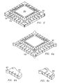
- Figure 3a illustrates the first surface of the tape 301 having an array of patterned leads 302 with contact pads 306, 307 on both ends.
- the tape is a thermally stable polymeric material from the polyimide family having good dielectric characteristics.
- Leads 302 and pads 306,307 are arrayed in each quadrant forming a square or rectangular pattern with a plurality of leads in each section.
- the outer pads 306 are larger than those on the opposite end, and provide the site for solder ball attachment.
- the smaller inner pads 307 provide contact locations for chip interconnection, either as wire bond lands, or bump pads.
- solder balls denote contacts to a printed wiring board or other next level interconnection, while bumps refer to chip contacts to a substrate or interposer.
- the chip contact bumps may be of solder, conductive adhesive, or other material known in the industry. Generally, the solder balls are larger in diameter than the bump connections.
- the outer pads 306 preferably are staggered to allow placement of larger solder balls, and the inner pads 307 may be staggered to mirror flip chip bump contacts, or may be in a single row, as illustrated in Figure 3a for perimeter flip chip contact, and/or for wire bond pads.
- the tape 301 is partially folded and formed into a package substrate.
- the tape has been inverted so that the metal pattern is face down, the corners have been slit, and each side is being folded inwardly so that the smaller pads 307 for wire bond or flip chip contact are positioned on the top surface of the device.
- Leads 302 extend around the formed substrate edge, and connect to solder ball pads on the bottom side of the substrate.
- Both the flexible tape and patterned metal are sufficiently malleable to allow folding so that chip pads and solder ball pads are on opposite surfaces.
- a preferred tape is a thermally stable polymer from the polyimide family, well known in the semiconductor industry for its low dielectric constant, and as the preferred material for various tape interconnection and packaging applications. Flex tape is preferably in the range of 0.001 to 0.003 inches thick.
- the preferred metal conductors includes a copper alloy with a thin film of nickel or other barrier metal, covered by a thin film of gold or other noble, solderable metal on the exposed surface.
- the inventive flex tape substrate is adaptable to flip chip interconnection, as well as to wire bonded devices.
- Figures 4a and 4b illustrate steps in the fabrication of a flip chip embodiment.
- the tape has been patterned and slit, and the substrate is partially formed by folding the corners of the unpatterned surfaces inwardly.
- the unpatterned surfaces of the folded tape are adhered together, or to a core member in order to provide a mechanically stable substrate.
- larger terminals 406 for solder balls are positioned on the folded sections 4011 of the substrate 401, and the chip contact terminals are on the underside or unfolded 4012 surface.
- the tape substrate 401 is inverted from the view in Figure 4a.
- a specific substrate design may accommodate either area array 408 or perimeter 409 bump interconnection to the chip.
- the tape is folded to expose the flip chip terminals on the folded sections of the substrate, and the larger solder bump terminals on the center surface, similar to the arrangement in figure 3b.
- Figure 5 shows the inventive single layer metal folded flex tape substrate 501 having a semiconductor device 503 connected by wire bonds 510. It can be seen that fine wires bonded to the chip pads are connected to bonding lands or pads 507 on the substrate. The assemblage will subsequently be encapsulated to protect the chip and bond wires, and solder balls will be attached to the pads on the underside.
- Figure 6a illustrates another embodiment of the flex tape 601 having a metal leads patterned on a single side formed around a rigid core 620 which preferably has high thermal conductivity, and thereby serves as a heat spreader.
- the core or heat spreader 620 of approximately the package external dimensions may include a thermally activated adhesive coating to secure the tape 601.
- the tape is formed around the core, heat and pressure applied to secure the tape and provide a stable, rigid substrate.
- the heat spreader core is preferably an alloy or clad metal, such as copper/invar/copper, or a thermally conductive ceramic having relatively low coefficient of thermal expansion (CTE).
- Either the low expansion clad metal or ceramic provide CTE match to the silicon chip, and are particularly well suited to flip chip applications wherein thermal stresses on small flip chip interconnection joints are of concern. Thickness of the heat spreader core is determined by geometric requirements of the finished semiconductor device. Because many devices have requirements for thickness, as well as overall package dimensions, thickness is preferably in the range of 0.005 to 0.020 inches.
- the core may include protrusions 621 in each corner which help in the protection of the exposed leads on the package sides from mechanical damage.
- Bonding lands, or pads 607 on the top side of the package provide sites for chip connections, and in Figure 6c, BGA pads 606 for solder balls on the bottom side of the package are staggered.
- a stress absorbing material is incorporated between the folded surfaces of the tape substrate.
- Different embodiments of the inventive substrate allow the stress absorbing material to be positioned on either or both sides of a stiff core or heat spreader, or between the folded tapes having no rigid core.
- Figure 7 is a cross section of a flip chip device having a chip 703 with solder bumps 708 and solder balls 705 attached to the patterned metal 707 on a flex tape 701 substrate.
- a rigid core 720 having a coefficient of thermal expansion similar to that of the chip 703 is in contact with the tape 701 on the top or chip side of the device.
- a stress absorbing material 730 is incorporated between the core 720 and tape 701 on the bottom or solder ball 705 side of the package in order to mitigate stresses on the solder joint which arise from CTE mismatch between the core and circuit board 780.
- the low modulus stress absorbing material preferably is thermally conductive, may be electrically conductive or insulating, may be an adhesive, or may be attached by an adhesive, and the thickness of the layer is largely a function of its elastic modulus.
- an underfill material 709 is added between the chip 703 and tape 701 substrate to further protect the chip interconnection joints.
- a layer of stress absorbing material 831 is incorporated within the folded substrate between the 801 tape and the rigid core 820 on the chip side.
- the layer 831 absorbs much of the stress on the bump 808 interconnection arising from thermal mismatch, while a similar layer 830 on the bottom side of the core protects the solder ball 805 joints.
- Figure 9 illustrates an embodiment wherein a chip 903 has wire bond 910 contacts to a tape 901 substrate having a rigid core 920.
- a layer of low modulus material 930 between the core and tape on the solder ball side relieves stress on the solder joints.
- the chip 903 is CTE matched to the core 920, and the rigid core provides stable bonding land sites 9071 for reliable wire bonds.
- Figure 10 is a cross section of a flip chip embodiment of the invention having no core material, and having a stress absorbing layer 1030 captured within the inert, folded surfaces of the tape 1001.
- the chip 1003 is the most rigid member of this device, and the stress absorbing layer 1030 protects both the solder ball 1005 and bump 1008 joints.
- a significant advantage of the continuous metal leads from chip to solder ball is that continuity of the interconnection is readily tested. Resistance of each lead is tested between pads 306 and 307, as shown in Figure 3 prior to folding the substrate. Those test results may be compared to values of the leads for the folded substrate, as shown in figures 3b and 4 to insure that there has been no performance deterioration. Elimination of vias with voids and other defects which plague existing area array substrates allows the finished devices to be reliably and inexpensively tested and analyzed.
Landscapes
- Wire Bonding (AREA)
Applications Claiming Priority (2)
| Application Number | Priority Date | Filing Date | Title |
|---|---|---|---|
| US200276 | 1980-10-24 | ||
| US10/200,276 US20040012078A1 (en) | 2002-07-22 | 2002-07-22 | Folded tape area array package with one metal layer |
Publications (2)
| Publication Number | Publication Date |
|---|---|
| EP1385208A2 true EP1385208A2 (de) | 2004-01-28 |
| EP1385208A3 EP1385208A3 (de) | 2004-03-10 |
Family
ID=30000068
Family Applications (1)
| Application Number | Title | Priority Date | Filing Date |
|---|---|---|---|
| EP03102100A Withdrawn EP1385208A3 (de) | 2002-07-22 | 2003-07-10 | Gefaltete bga-band packung mit einer metallschicht |
Country Status (3)
| Country | Link |
|---|---|
| US (1) | US20040012078A1 (de) |
| EP (1) | EP1385208A3 (de) |
| JP (1) | JP2004056135A (de) |
Families Citing this family (15)
| Publication number | Priority date | Publication date | Assignee | Title |
|---|---|---|---|---|
| US7242082B2 (en) * | 2002-02-07 | 2007-07-10 | Irvine Sensors Corp. | Stackable layer containing ball grid array package |
| US6967411B2 (en) * | 2002-02-07 | 2005-11-22 | Irvine Sensors Corporation | Stackable layers containing ball grid array packages |
| US7268425B2 (en) * | 2003-03-05 | 2007-09-11 | Intel Corporation | Thermally enhanced electronic flip-chip packaging with external-connector-side die and method |
| JP3846437B2 (ja) * | 2003-03-17 | 2006-11-15 | 株式会社日立製作所 | 自動車用コントロールユニット |
| US20040246008A1 (en) * | 2003-06-04 | 2004-12-09 | Barr Andrew H. | Apparatus and method for detecting and rejecting high impedance interconnect failures in manufacturing process |
| US6940288B2 (en) * | 2003-06-04 | 2005-09-06 | Hewlett-Packard Development Company, L.P. | Apparatus and method for monitoring and predicting failures in system interconnect |
| US7112877B2 (en) * | 2004-06-28 | 2006-09-26 | General Electric Company | High density package with wrap around interconnect |
| US8178901B2 (en) * | 2005-04-28 | 2012-05-15 | St-Ericsson Sa | Integrated circuit assembly with passive integration substrate for power and ground line routing on top of an integrated circuit chip |
| US7170183B1 (en) * | 2005-05-13 | 2007-01-30 | Amkor Technology, Inc. | Wafer level stacked package |
| US8541876B2 (en) * | 2005-09-30 | 2013-09-24 | Intel Corporation | Microelectronic package having direct contact heat spreader and method of manufacturing same |
| US7684205B2 (en) * | 2006-02-22 | 2010-03-23 | General Dynamics Advanced Information Systems, Inc. | System and method of using a compliant lead interposer |
| US7990727B1 (en) | 2006-04-03 | 2011-08-02 | Aprolase Development Co., Llc | Ball grid array stack |
| US7714426B1 (en) * | 2007-07-07 | 2010-05-11 | Keith Gann | Ball grid array package format layers and structure |
| US8829685B2 (en) * | 2009-03-31 | 2014-09-09 | Semiconductor Components Industries, Llc | Circuit device having funnel shaped lead and method for manufacturing the same |
| US20130308274A1 (en) * | 2012-05-21 | 2013-11-21 | Triquint Semiconductor, Inc. | Thermal spreader having graduated thermal expansion parameters |
Family Cites Families (3)
| Publication number | Priority date | Publication date | Assignee | Title |
|---|---|---|---|---|
| US5072283A (en) * | 1988-04-12 | 1991-12-10 | Bolger Justin C | Pre-formed chip carrier cavity package |
| US5148265A (en) * | 1990-09-24 | 1992-09-15 | Ist Associates, Inc. | Semiconductor chip assemblies with fan-in leads |
| US5278724A (en) * | 1992-07-06 | 1994-01-11 | International Business Machines Corporation | Electronic package and method of making same |
-
2002
- 2002-07-22 US US10/200,276 patent/US20040012078A1/en not_active Abandoned
-
2003
- 2003-07-10 EP EP03102100A patent/EP1385208A3/de not_active Withdrawn
- 2003-07-22 JP JP2003199944A patent/JP2004056135A/ja active Pending
Also Published As
| Publication number | Publication date |
|---|---|
| EP1385208A3 (de) | 2004-03-10 |
| JP2004056135A (ja) | 2004-02-19 |
| US20040012078A1 (en) | 2004-01-22 |
Similar Documents
| Publication | Publication Date | Title |
|---|---|---|
| US5627405A (en) | Integrated circuit assembly incorporating an anisotropic elecctrically conductive layer | |
| JP3772066B2 (ja) | 半導体装置 | |
| JP3335575B2 (ja) | 半導体装置およびその製造方法 | |
| US6815254B2 (en) | Semiconductor package with multiple sides having package contacts | |
| KR100252731B1 (ko) | 반도체 디바이스 및 반도체 디바이스용 패키지 | |
| US7378731B2 (en) | Heat spreader and package structure utilizing the same | |
| JP3999720B2 (ja) | 半導体装置およびその製造方法 | |
| US20030164551A1 (en) | Method and apparatus for flip-chip packaging providing testing capability | |
| US6507095B1 (en) | Wiring board, connected board and semiconductor device, method of manufacture thereof, circuit board, and electronic instrument | |
| EP1385208A2 (de) | Gefaltete bga-band packung mit einer metallschicht | |
| KR20010070217A (ko) | 반도체 장치 및 그 제조 방법 | |
| WO1999023696A1 (en) | Semiconductor device and method for manufacturing the same______ | |
| EP1025585A1 (de) | Verfahren und konstruktion einer thermisch verbesserten mikroelektronischen packung | |
| KR20010072583A (ko) | 적층화 집적 회로 패키지 | |
| KR20180077046A (ko) | 반도체 장치 | |
| US20070228566A1 (en) | Ball grid array package construction with raised solder ball pads | |
| US7344916B2 (en) | Package for a semiconductor device | |
| KR20090022659A (ko) | 집적회로 패키지 및 그 제조방법 | |
| KR100614431B1 (ko) | 개선된 수율의 반도체 패키지 디바이스를 제조하기 위한 구조 및 방법 | |
| JPH11204560A (ja) | 半導体装置及びその製造方法 | |
| CN101393250A (zh) | 用于晶片级半导体测试的测试座及测试板 | |
| JP4498336B2 (ja) | 半導体装置および半導体装置の製造方法 | |
| JP3841135B2 (ja) | 半導体装置、回路基板及び電子機器 | |
| JP3923944B2 (ja) | 半導体装置 | |
| KR100592785B1 (ko) | 칩 스케일 패키지를 적층한 적층 패키지 |
Legal Events
| Date | Code | Title | Description |
|---|---|---|---|
| PUAI | Public reference made under article 153(3) epc to a published international application that has entered the european phase |
Free format text: ORIGINAL CODE: 0009012 |
|
| PUAL | Search report despatched |
Free format text: ORIGINAL CODE: 0009013 |
|
| AK | Designated contracting states |
Kind code of ref document: A2 Designated state(s): AT BE BG CH CY CZ DE DK EE ES FI FR GB GR HU IE IT LI LU MC NL PT RO SE SI SK TR |
|
| AX | Request for extension of the european patent |
Extension state: AL LT LV MK |
|
| AK | Designated contracting states |
Kind code of ref document: A3 Designated state(s): AT BE BG CH CY CZ DE DK EE ES FI FR GB GR HU IE IT LI LU MC NL PT RO SE SI SK TR |
|
| AX | Request for extension of the european patent |
Extension state: AL LT LV MK |
|
| 17P | Request for examination filed |
Effective date: 20040910 |
|
| 17Q | First examination report despatched |
Effective date: 20041013 |
|
| AKX | Designation fees paid |
Designated state(s): DE FR GB |
|
| STAA | Information on the status of an ep patent application or granted ep patent |
Free format text: STATUS: THE APPLICATION IS DEEMED TO BE WITHDRAWN |
|
| 18D | Application deemed to be withdrawn |
Effective date: 20050426 |