EP1378824A1 - Procédé d'exécution de programmes dans un système multiprocesseurs, et système de processeur correspondant - Google Patents
Procédé d'exécution de programmes dans un système multiprocesseurs, et système de processeur correspondant Download PDFInfo
- Publication number
- EP1378824A1 EP1378824A1 EP02425436A EP02425436A EP1378824A1 EP 1378824 A1 EP1378824 A1 EP 1378824A1 EP 02425436 A EP02425436 A EP 02425436A EP 02425436 A EP02425436 A EP 02425436A EP 1378824 A1 EP1378824 A1 EP 1378824A1
- Authority
- EP
- European Patent Office
- Prior art keywords
- vliw
- processor
- instruction
- instructions
- processors
- Prior art date
- Legal status (The legal status is an assumption and is not a legal conclusion. Google has not performed a legal analysis and makes no representation as to the accuracy of the status listed.)
- Withdrawn
Links
- 238000000034 method Methods 0.000 title claims description 65
- 238000012545 processing Methods 0.000 claims abstract description 8
- 230000008569 process Effects 0.000 claims description 58
- 230000015654 memory Effects 0.000 claims description 30
- 230000006870 function Effects 0.000 claims description 7
- 230000004913 activation Effects 0.000 claims description 2
- 230000000750 progressive effect Effects 0.000 claims description 2
- 230000006837 decompression Effects 0.000 claims 1
- 230000004048 modification Effects 0.000 claims 1
- 238000012986 modification Methods 0.000 claims 1
- 238000010586 diagram Methods 0.000 description 19
- 230000008859 change Effects 0.000 description 5
- 101150039208 KCNK3 gene Proteins 0.000 description 3
- 238000013459 approach Methods 0.000 description 2
- 230000008901 benefit Effects 0.000 description 2
- 230000001419 dependent effect Effects 0.000 description 2
- 238000010521 absorption reaction Methods 0.000 description 1
- 238000005352 clarification Methods 0.000 description 1
- 230000000295 complement effect Effects 0.000 description 1
- 238000005265 energy consumption Methods 0.000 description 1
- 230000008520 organization Effects 0.000 description 1
- 230000002093 peripheral effect Effects 0.000 description 1
- 238000009877 rendering Methods 0.000 description 1
- 238000012546 transfer Methods 0.000 description 1
- 238000012795 verification Methods 0.000 description 1
Images


Classifications
-
- G—PHYSICS
- G06—COMPUTING; CALCULATING OR COUNTING
- G06F—ELECTRIC DIGITAL DATA PROCESSING
- G06F9/00—Arrangements for program control, e.g. control units
- G06F9/06—Arrangements for program control, e.g. control units using stored programs, i.e. using an internal store of processing equipment to receive or retain programs
- G06F9/30—Arrangements for executing machine instructions, e.g. instruction decode
- G06F9/38—Concurrent instruction execution, e.g. pipeline or look ahead
- G06F9/3877—Concurrent instruction execution, e.g. pipeline or look ahead using a slave processor, e.g. coprocessor
- G06F9/3879—Concurrent instruction execution, e.g. pipeline or look ahead using a slave processor, e.g. coprocessor for non-native instruction execution, e.g. executing a command; for Java instruction set
-
- G—PHYSICS
- G06—COMPUTING; CALCULATING OR COUNTING
- G06F—ELECTRIC DIGITAL DATA PROCESSING
- G06F9/00—Arrangements for program control, e.g. control units
- G06F9/06—Arrangements for program control, e.g. control units using stored programs, i.e. using an internal store of processing equipment to receive or retain programs
- G06F9/30—Arrangements for executing machine instructions, e.g. instruction decode
- G06F9/38—Concurrent instruction execution, e.g. pipeline or look ahead
- G06F9/3836—Instruction issuing, e.g. dynamic instruction scheduling or out of order instruction execution
- G06F9/3853—Instruction issuing, e.g. dynamic instruction scheduling or out of order instruction execution of compound instructions
-
- G—PHYSICS
- G06—COMPUTING; CALCULATING OR COUNTING
- G06F—ELECTRIC DIGITAL DATA PROCESSING
- G06F9/00—Arrangements for program control, e.g. control units
- G06F9/06—Arrangements for program control, e.g. control units using stored programs, i.e. using an internal store of processing equipment to receive or retain programs
- G06F9/30—Arrangements for executing machine instructions, e.g. instruction decode
- G06F9/38—Concurrent instruction execution, e.g. pipeline or look ahead
- G06F9/3877—Concurrent instruction execution, e.g. pipeline or look ahead using a slave processor, e.g. coprocessor
Definitions
- the present invention relates to processors and methods for processing signals that can be implemented using said processors.
- the most widely used architecture consists of a system made up of two processors.
- the first processor which is specialized in handling the part with the largest computational burden, typically consists of a Digital Signal Processor or DSP.
- DSP Digital Signal Processor
- the other processor with tasks of control, synchronization and execution of high-level applications, is typically configured as a CPU.
- FIG. 1 An example of architecture of this sort is illustrated in Figure 1, where the aforesaid processors, designated respectively by DSP and CPU 1, are illustrated together with the cache memories associated thereto, namely together with instruction cache memories 1$ and data cache memories D$, respectively.
- CMC Designated by CMC are the interface modules, referred to as Core Memory Controllers, which enable two sub-systems coming under the two processors DSP and CPU 1 to interface with one another by means of a main bus B with the main system memory MEM and with the various peripheral units PI, P2, P3, P4, ... associated to the system.
- Core Memory Controllers the interface modules, referred to as Core Memory Controllers, which enable two sub-systems coming under the two processors DSP and CPU 1 to interface with one another by means of a main bus B with the main system memory MEM and with the various peripheral units PI, P2, P3, P4, ... associated to the system.
- the CPU 1 is typically a 32-bit pipelined scalar microprocessor.
- pipelined scalar is meant that its internal architecture is made up of different logic stages, each of which contains an instruction in a very specific state. The said state may be that of:
- the number of bits on which the CPU 1 operates is related to the width of the data on which the machine is operating.
- the instructions are generated and executed in turn, in a specific order defined by compiling.
- the other processor is typically a superscalar microprocessor or 128-bit pipelined VLIW (acronym for Very Long Instruction Word) microprocessor.
- VLIW Very Long Instruction Word
- "Pipelined superscalar” means that its internal architecture is made up of different logic stages, some of the which are able to execute instructions in parallel, for example in the execution step.
- the parallelism is of four instructions each (equal to 128 bit) whilst the data are expressed in 32 bits.
- the processor is said to be superscalar if the instructions are re-ordered dynamically in the execution step in order to supply the execution stages which can potentially work in parallel, also altering the order generated statically by compiling of the source code, if the instructions do not present any mutual dependence.
- the main disadvantage of this approach lies in the complexity of the resulting machine, in which the logic of scheduling of the instructions may prove one of the most important parts in terms of number of gates.
- VLIW processor is used if the instructions are re-ordered statically in the compiling step and executed in the pre-set order, which is not modifiable in the execution step.
- the advantage of the said approach is that it eliminates all the logic of management of the scheduling since this task is performed during compiling.
- the main disadvantage lies in the fact that the compiled code is strictly dependent upon the implementation of the machine on which it is executed. For example, given the same instruction-set architecture (ISA), a machine with N execution units cannot execute a compiled code for a machine with K execution units if K is not equal to N. From this it follows that there is no "binary compatibility" between different generations of processors with the same ISA.
- ISA instruction-set architecture
- binary compatibility is meant the property existing between a group of processors each of which is able to execute one and the same binary machine-code datum.
- each processor possesses its own data cache D$ and its own instruction cache I$, so as to be able to load from the main memory MEM both the data on which to operate and the instructions to be executed in parallel. Since the two processors CPU 1 and DSP are connected to the main memory MEM through the system bus B, the two processors are typically found competing for access to said memory when an instruction and/or the data on which they are to operate must be located in the main memory, the said instruction or data not being available in their own caches.
- a system based upon the architecture represented in Figure 1 has a sharing of work and of processes that is rigid and not modifiable, such as to render asymmetrical the workload and the software programs to be executed.
- a processor such as the CPU 1 usually possesses 16 Kbytes of data cache and 16 Kbytes of instruction cache, whereas the DSP usually possesses 32 Kbytes of data cache and 32 Kbytes of instruction cache.
- the flowchart of Figure 2 illustrates the logic diagram of the CPU described from top to bottom.
- the first stage designated by 10, generates the memory address to which the instruction to be executed is associated, the said address being referred to as program counter.
- the stage 10 is hence configured typically as a fetch stage, whilst the instruction thus loaded is decoded in the stage 12 separating the bit field which defines its function (for example, addition of 2 values contained in two registers located in the register file) with respect to the bit fields which address the operands.
- the said addresses are sent to a register file from which (in a stage designated by 14) are read the operands of the instruction.
- the operands and the bits which define the function to be executed are sent to the execution unit which, in a stage 16, performs the desired operation, for example the operation of addition referred to previously.
- the result can thus be re-stored in the register file in a stage 18 currently called write-back stage.
- the process schematically represented in Figure 2 operates in combination with a load/store unit which enables reading/writing of any possible data in memory with the aid of specific instructions dedicated to the purpose.
- the set of instructions is in biunique correspondence with a given microprocessing CPU architecture.
- the flowchart of Figure 3 shows, instead, the logic diagram of the DSP. Also in this case, there is envisaged an initial fetch stage 20, associated to which there is logically cascaded a stage 20a for issuing instructions.
- the reference number 22 designates, instead, a decoding stage whilst the reference number 24 designates a register file (see the stages 14 and 16 of Figure 2).
- the reference number 28 designates a stage for re-storage in the register file, which is in general akin to the stage 18 of Figure 1.
- the reference number 26 designates collectively a plurality of execution stages that can be executed in parallel.
- references OsTask 1.1, 1.2, etc. illustrate processes which can be executed by the processor CPU 1.
- the first processes contain instructions generated by the compiler of the processor CPU 1 and hence can be executed by the latter, but not by the DSP.
- the situation is exactly complementary, in the sense that they contain instructions generated by the compiler of the DSP and can hence be executed by the said processor, but not by the other processor CPU 1.
- processor CPU 1 is characterized by a compiling flow of its own, which is independent of and distinct from that of the DSP.
- processor CPU 1 could even be turned off when not in use, so enabling a considerable energy saving.
- the latencies introduced vary from tens of microseconds to tens or hundreds of milliseconds.
- the above latencies prove particularly costly, both from the energy standpoint and from the computational standpoint.
- the DSP is forced to work at approximately 90% of its computational capacity. This implies an evident asymmetry in the workload of the processor CPU as compared to the workload of the DSP, an asymmetry which is revealed also in the power-management algorithms, which are distinct for the two processors.
- the purpose of the present invention is to provide a solution capable of overcoming the drawbacks outlined previously.
- the said purpose is achieved thanks to a procedure having the characteristics referred to specifically in the claims that follow.
- the invention also regards the corresponding processor system, in particular multiprocessor system.
- the present invention thus offers a solution, which enables:
- the solution according to the invention makes it possible to provide a multiprocessing architecture comprising a plurality of processors.
- processors considered are all of the VLIW type.
- the solution according to the invention is, however, applicable, for example, to architectures comprising one or more VLIW processors in combination with at least one superscalar processor, the only important aspect being that the processors in question should have the same instruction-set architecture (ISA).
- ISA instruction-set architecture
- the solution according to the invention is in fact based upon the recognition of certain essential facts.
- Each VLIW processor can execute instructions with a different maximum length; for example, the first can execute at the most four basic instructions in parallel for each clock cycle, whilst the second can use at the most eight instructions in parallel for each clock cycle.
- Each processor has a unit for issuing instructions, which typically reads from the instruction cache a number of instructions equal to the number that it is able to handle in parallel. For example, if the processor is able to handle in parallel up to four instructions, the corresponding unit for issuing instructions may read simultaneously up to four instructions but not more.
- a second VLIW processor a modified-instruction unit which is able to read at input words corresponding to very long instructions originally compiled with a view to their execution on a first VLIW processor and to issue at output words corresponding to very long instructions ready to be executed on the second VLIW processor.
- each instruction in the very long instruction word has in fact been scheduled by the compiler in such a way as to be independent from the others.
- This result is obtained in the form of a cascade of simple splitting operations and of entry of fictitious (no-operation) instructions according to the length of the instructions of any single VLIW processor.
- a table which stores the information corresponding to each process in terms (it may amount to a simple order number) which identify the VLIW processor for which it has been compiled, together with an identifier (also in this case it may simply be a number) which identifies the last VLIW processor on which, within the plurality of processors comprising the multi-processor architecture, the process has been executed, as well as of course the co-ordinates for tracing the context of the process in the main memory.
- Context of a processor is here meant to indicate basically:
- the solution according to the invention solves a major problem in the framework of VLIW processors, namely, that of binary compatibility between architectures and different parallelisms, enabling for example the dynamic transfer of the process workload between VLIW processors that are symmetrical from the point of view of the instruction set and asymmetrical in terms of parallelism of instruction.
- the diagram of Figure 6 is intrinsically symmetrical, in so far as it envisages the presence of two (or more) processors of a VLIW type here designated, respectively, as VLIW 1 and VLIW 2, which, albeit instantiated according to different criteria, operate in conditions of substantial symmetry, in so far they are able to execute the same processes, without this requiring recompiling or duplication of the object codes for the two processors, it being at the same time altogether possible to allow for the presence of two (or more) VLIW processors having different hardware parallelisms.
- VLIW have the same instruction-set architecture (ISA). This means that they are defined by the same list of instructions, syntax and semantics, and length (for example 32 bits per basic instruction).
- Figure 8 shows how the aim is to associate statically and dynamically each of the processes indifferently on each of the two processors VLIW 1 and VLIW 2 on the basis of decisions that can change dynamically. These may, for example, be decisions based upon the dynamic load of each of the processors, upon the dynamic operating frequency, and upon instantaneous energy consumption, the final purpose being to split the workload evenly on the two processors.
- each of the two (or more) processors considered is able to function with a different working frequency, so that each processor may dynamically change the operating frequency without jeopardizing its proper operation.
- the Task1 as shown in Figure 7, is compiled for generating a flow of long instructions with a maximum length of four, assuming that they are to be executed on the processor VLIW 1.
- the Task2 is, instead, compiled for generating a flow of long instructions with a maximum length of eight, assuming that the intention is to execute them on the processor VLIW 2.
- FIG 9 shows how the so-called instruction-issue unit (IIU) of a processor, as noted in Figure 3, has to be modified for carrying out the following task with the purpose of ensuring binary compatibility without duplicating the object code.
- IIU instruction-issue unit
- VLIW 1 receives instructions that are 8 ⁇ 32 bits long whereas the processor is able to execute at the most 4 ⁇ 32 bits per cycle.
- the IIU will thus have to split the instructions at input into two instructions that are 4 ⁇ 32 bits long.
- the IIU in question must thus lengthen the input instruction by means of 4 ⁇ 32 bit null instructions of the no-operation (nop) type.
- a typical example (well known to persons skilled in the sector) of a nop instruction is the instruction for carrying out the addition of the number 0 with itself to be written in the register that contains the said 0, which is one just for reading. It is therefore an instruction that expresses a deliberate nonsense. Furthermore, the nop instructions cause switching-off of four of the eight functional units, so reducing the power consumption of the processor VLIW 2.
- Figure 9 illustrates a further example of what has been said above, an example which relates specifically to the case where L1 is equal to 4 and L2 is equal to 8.
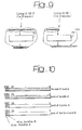
- Another solution which refers specifically to Figures 10 and 11, may consist in rendering explicit, in the machine instructions of the processor, different bits referred to as "stop-bundle" bits corresponding to different word lengths, i.e., different maximum levels of parallelism executable by the machine.
- a processor built with parallelism A uses as stop-bundle indicator the bit 31, ignoring the bit 30.
- a processor built with parallelism B uses as stop-bundle-indicator the bit 30, ignoring the bit 31.
- the verification of the end of bundle is made normally at the level of instruction-issue unit (IIU), since each processor has an associated instruction cache I$ and (potentially) a compressor/decompressor of the code to be executed.
- IIU instruction-issue unit
- the operation of placing the appropriate stop bundle in the "effective" instruction bit can be carried out according to the parallelism of the machine which is executing the code.
- the parallelism of the machine which is executing the code see Figure 11.
- the situation represented in Part B of Figure 11 refers instead to execution on a machine with width 4.
- the stop bundle for the width of 4 is placed in the instruction corresponding to the bit 31.
- the above comprises the consequent possibility of rejecting the part of appendix IA, so as to give rise to an instruction format represented in Part C again of Figure 11.
- the module which performs the operation just described is defined as "instruction-formatting" module or "instruction formatter”.
- the compiler In the compiling step, then, the compiler generates all the additional (stop-bundle) information for all the output widths envisaged in the instruction appendix IA.
- the above will then be used by the formatter IF according to the configuration thereof.
- the operation performed by the formatter IF consists only in entering a bit and eliminating the appendix IA. These are operations which can be implemented in an elementary way at the hardware level, as will be evident to persons skilled in the sector.
- the solution according to the invention offers the important advantage provided by the complete binary compatibility between the two (or more) processors, this compatibility being understood as capacity for executing indistinctly said process on the various VLIW processors comprised in a multiprocessor system using the same compiled code without any needless duplications.
- the said capacity moreover enables dynamic distribution of the computational load on the various processors so as to be able to equalize the operating frequency of the processors themselves with respect to the maximum point. There is thus achieved a saving in dissipated power which, as is known, is linearly dependent upon the operating frequency of the processor.
- the above table is accessible by a process referred to as control process, which is executed for a pre-set time on each of the VLIW processors.
- each processor has thus the possibility of consulting and updating the table in order to equalize its own workload with respect to the second processor.
- the said table likewise contains the co-ordinates whereby a processor can take possession of and execute one of the processes listed.
Landscapes
- Engineering & Computer Science (AREA)
- Software Systems (AREA)
- Theoretical Computer Science (AREA)
- Physics & Mathematics (AREA)
- General Engineering & Computer Science (AREA)
- General Physics & Mathematics (AREA)
- Devices For Executing Special Programs (AREA)
- Advance Control (AREA)
Priority Applications (4)
| Application Number | Priority Date | Filing Date | Title |
|---|---|---|---|
| EP02425436A EP1378824A1 (fr) | 2002-07-02 | 2002-07-02 | Procédé d'exécution de programmes dans un système multiprocesseurs, et système de processeur correspondant |
| US10/612,825 US7617494B2 (en) | 2002-07-02 | 2003-07-01 | Process for running programs with selectable instruction length processors and corresponding processor system |
| US10/612,831 US7395532B2 (en) | 2002-07-02 | 2003-07-01 | Process for running programs on processors and corresponding processor system |
| US12/147,999 US8176478B2 (en) | 2002-07-02 | 2008-06-27 | Process for running programs on processors and corresponding processor system |
Applications Claiming Priority (1)
| Application Number | Priority Date | Filing Date | Title |
|---|---|---|---|
| EP02425436A EP1378824A1 (fr) | 2002-07-02 | 2002-07-02 | Procédé d'exécution de programmes dans un système multiprocesseurs, et système de processeur correspondant |
Publications (1)
| Publication Number | Publication Date |
|---|---|
| EP1378824A1 true EP1378824A1 (fr) | 2004-01-07 |
Family
ID=29719820
Family Applications (1)
| Application Number | Title | Priority Date | Filing Date |
|---|---|---|---|
| EP02425436A Withdrawn EP1378824A1 (fr) | 2002-07-02 | 2002-07-02 | Procédé d'exécution de programmes dans un système multiprocesseurs, et système de processeur correspondant |
Country Status (2)
| Country | Link |
|---|---|
| US (3) | US7395532B2 (fr) |
| EP (1) | EP1378824A1 (fr) |
Families Citing this family (13)
| Publication number | Priority date | Publication date | Assignee | Title |
|---|---|---|---|---|
| EP1378824A1 (fr) | 2002-07-02 | 2004-01-07 | STMicroelectronics S.r.l. | Procédé d'exécution de programmes dans un système multiprocesseurs, et système de processeur correspondant |
| US7788255B2 (en) * | 2004-01-21 | 2010-08-31 | Oracle International Corporation | Specifying parallel or sequential execution of database operations by bundling database statements |
| JP4283131B2 (ja) * | 2004-02-12 | 2009-06-24 | パナソニック株式会社 | プロセッサ及びコンパイル方法 |
| US7788671B2 (en) * | 2004-11-01 | 2010-08-31 | International Business Machines Corporation | On-demand application resource allocation through dynamic reconfiguration of application cluster size and placement |
| JP2006243838A (ja) * | 2005-02-28 | 2006-09-14 | Toshiba Corp | プログラム開発装置 |
| US7525548B2 (en) * | 2005-11-04 | 2009-04-28 | Nvidia Corporation | Video processing with multiple graphical processing units |
| US7768517B2 (en) * | 2006-02-21 | 2010-08-03 | Nvidia Corporation | Asymmetric multi-GPU processing |
| US9405564B2 (en) * | 2006-05-10 | 2016-08-02 | The Mathworks, Inc. | System and method for targeting commands to concurrent computing units executing a concurrent computing process |
| US7631168B1 (en) | 2006-05-10 | 2009-12-08 | The Math Works, Inc. | Graphical interface for grouping concurrent computing units executing a concurrent computing process |
| JP5435133B2 (ja) * | 2010-07-13 | 2014-03-05 | 富士通株式会社 | 情報処理装置、情報処理装置の制御方法及びプログラム |
| JP5367020B2 (ja) * | 2011-06-24 | 2013-12-11 | 株式会社ソニー・コンピュータエンタテインメント | 情報処理装置、情報処理方法、プログラム及び情報記憶媒体 |
| WO2016193774A1 (fr) * | 2015-06-01 | 2016-12-08 | Intel Corporation | Processeur multicœur pour l'exécution de fils d'instructions groupés selon leur criticité |
| US9658837B1 (en) * | 2015-11-06 | 2017-05-23 | Sentry Insurance a Mutual Company | Integration of independent platforms |
Citations (4)
| Publication number | Priority date | Publication date | Assignee | Title |
|---|---|---|---|---|
| EP0768602A2 (fr) * | 1995-10-13 | 1997-04-16 | Matsushita Electric Industrial Co., Ltd. | Processeur des instructions VLIW de longueur variable |
| WO2000033186A1 (fr) * | 1998-12-03 | 2000-06-08 | Sun Microsystems, Inc. | Processeur a mot d'instruction tres long a largeur de production variable |
| WO2001053933A2 (fr) * | 2000-01-19 | 2001-07-26 | Micron Technology, Inc. | Processeur divise a memoire dram integree |
| EP1152329A1 (fr) * | 2000-03-30 | 2001-11-07 | Agere Systems Guardian Corporation | Procédé et dispositif d'identification de paquets séparables dans un processeur multifilière vliw |
Family Cites Families (30)
| Publication number | Priority date | Publication date | Assignee | Title |
|---|---|---|---|---|
| CA1293819C (fr) * | 1986-08-29 | 1991-12-31 | Thinking Machines Corporation | Ordinateur a tres grande echelle |
| US5031096A (en) | 1988-06-30 | 1991-07-09 | International Business Machines Corporation | Method and apparatus for compressing the execution time of an instruction stream executing in a pipelined processor |
| US5634135A (en) | 1991-12-13 | 1997-05-27 | Texas Instruments Incorporated | Microprocessor with priority determination and priority based instruction selection |
| EP1186995B1 (fr) * | 1993-11-05 | 2003-09-03 | Intergraph Corporation | Mémoire d'instructions avec commutateur crossbar associatif |
| DE69428004T2 (de) | 1993-11-05 | 2002-04-25 | Intergraph Corp | Superskalare Rechnerarchitektur mit Softwarescheduling |
| US5669001A (en) | 1995-03-23 | 1997-09-16 | International Business Machines Corporation | Object code compatible representation of very long instruction word programs |
| JP3598589B2 (ja) * | 1995-06-28 | 2004-12-08 | 株式会社日立製作所 | プロセッサ |
| JP3623840B2 (ja) * | 1996-01-31 | 2005-02-23 | 株式会社ルネサステクノロジ | データ処理装置及びマイクロプロセッサ |
| JPH09265397A (ja) * | 1996-03-29 | 1997-10-07 | Hitachi Ltd | Vliw命令用プロセッサ |
| US5787302A (en) * | 1996-05-15 | 1998-07-28 | Philips Electronic North America Corporation | Software for producing instructions in a compressed format for a VLIW processor |
| US6272481B1 (en) * | 1996-05-31 | 2001-08-07 | Lucent Technologies Inc. | Hospital-based integrated medical computer system for processing medical and patient information using specialized functional modules |
| US6298370B1 (en) * | 1997-04-04 | 2001-10-02 | Texas Instruments Incorporated | Computer operating process allocating tasks between first and second processors at run time based upon current processor load |
| US6219779B1 (en) * | 1997-06-16 | 2001-04-17 | Matsushita Electric Industrial Co., Ltd. | Constant reconstructing processor which supports reductions in code size |
| JP3327818B2 (ja) | 1997-08-29 | 2002-09-24 | 松下電器産業株式会社 | プログラム変換装置及び記録媒体 |
| GB2332075B (en) * | 1997-12-06 | 2002-08-07 | Mitel Corp | Optimized instruction storage and distribution for parallel processors architectures |
| EP0924603A3 (fr) | 1997-12-16 | 2001-02-07 | Lucent Technologies Inc. | Planification dynamique d'instructions de programme sur commande de compilateur |
| US6324639B1 (en) * | 1998-03-30 | 2001-11-27 | Matsushita Electric Industrial Co., Ltd. | Instruction converting apparatus using parallel execution code |
| US6988183B1 (en) | 1998-06-26 | 2006-01-17 | Derek Chi-Lan Wong | Methods for increasing instruction-level parallelism in microprocessors and digital system |
| JP3224782B2 (ja) | 1998-08-03 | 2001-11-05 | インターナショナル・ビジネス・マシーンズ・コーポレーション | 処理分担動的変更方法及びコンピュータ |
| JP2001034471A (ja) | 1999-07-19 | 2001-02-09 | Mitsubishi Electric Corp | Vliw方式プロセッサ |
| US6799266B1 (en) | 1999-12-30 | 2004-09-28 | Texas Instruments Incorporated | Methods and apparatus for reducing the size of code with an exposed pipeline by encoding NOP operations as instruction operands |
| GB0012352D0 (en) | 2000-05-22 | 2000-07-12 | Northern Telecom Ltd | Reliable hardware support for the use of formal languages in high assurance systems |
| US6950926B1 (en) | 2001-03-02 | 2005-09-27 | Advanced Micro Devices, Inc. | Use of a neutral instruction as a dependency indicator for a set of instructions |
| WO2003003197A2 (fr) * | 2001-06-28 | 2003-01-09 | Oak Technology, Inc. | Unite de commande de systeme sur puce |
| EP1324191A1 (fr) | 2001-12-27 | 2003-07-02 | STMicroelectronics S.r.l. | Architecture et système de processeur, et procédé d'utilisation |
| US7062634B1 (en) * | 2002-01-29 | 2006-06-13 | Stmicroelectronics Limited | Processor and a method for handling and encoding no-operation instructions |
| US7200738B2 (en) * | 2002-04-18 | 2007-04-03 | Micron Technology, Inc. | Reducing data hazards in pipelined processors to provide high processor utilization |
| JP3738842B2 (ja) * | 2002-06-04 | 2006-01-25 | 富士通株式会社 | 遅延分岐機能を備えた情報処理装置 |
| JP3851228B2 (ja) * | 2002-06-14 | 2006-11-29 | 松下電器産業株式会社 | プロセッサ、プログラム変換装置及びプログラム変換方法、並びにコンピュータプログラム |
| EP1378824A1 (fr) | 2002-07-02 | 2004-01-07 | STMicroelectronics S.r.l. | Procédé d'exécution de programmes dans un système multiprocesseurs, et système de processeur correspondant |
-
2002
- 2002-07-02 EP EP02425436A patent/EP1378824A1/fr not_active Withdrawn
-
2003
- 2003-07-01 US US10/612,831 patent/US7395532B2/en active Active
- 2003-07-01 US US10/612,825 patent/US7617494B2/en not_active Expired - Fee Related
-
2008
- 2008-06-27 US US12/147,999 patent/US8176478B2/en active Active
Patent Citations (4)
| Publication number | Priority date | Publication date | Assignee | Title |
|---|---|---|---|---|
| EP0768602A2 (fr) * | 1995-10-13 | 1997-04-16 | Matsushita Electric Industrial Co., Ltd. | Processeur des instructions VLIW de longueur variable |
| WO2000033186A1 (fr) * | 1998-12-03 | 2000-06-08 | Sun Microsystems, Inc. | Processeur a mot d'instruction tres long a largeur de production variable |
| WO2001053933A2 (fr) * | 2000-01-19 | 2001-07-26 | Micron Technology, Inc. | Processeur divise a memoire dram integree |
| EP1152329A1 (fr) * | 2000-03-30 | 2001-11-07 | Agere Systems Guardian Corporation | Procédé et dispositif d'identification de paquets séparables dans un processeur multifilière vliw |
Also Published As
| Publication number | Publication date |
|---|---|
| US20080270769A1 (en) | 2008-10-30 |
| US7617494B2 (en) | 2009-11-10 |
| US20040059894A1 (en) | 2004-03-25 |
| US20040054882A1 (en) | 2004-03-18 |
| US8176478B2 (en) | 2012-05-08 |
| US7395532B2 (en) | 2008-07-01 |
Similar Documents
| Publication | Publication Date | Title |
|---|---|---|
| US8176478B2 (en) | Process for running programs on processors and corresponding processor system | |
| US6490673B1 (en) | Processor, compiling apparatus, and compile program recorded on a recording medium | |
| US6408382B1 (en) | Methods and apparatus for abbreviated instruction sets adaptable to configurable processor architecture | |
| CA2337172C (fr) | Methode et appareillage pour attribuer des unites fonctionnelles dans un processeur vliw multifiliere | |
| JP4841861B2 (ja) | 演算処理装置及びデータ転送処理の実行方法 | |
| US6950926B1 (en) | Use of a neutral instruction as a dependency indicator for a set of instructions | |
| US20050198476A1 (en) | Parallel multithread processor (PMT) with split contexts | |
| KR20180020985A (ko) | 디커플링된 프로세서 명령어 윈도우 및 피연산자 버퍼 | |
| JPH06230969A (ja) | プロセッサ | |
| US7574583B2 (en) | Processing apparatus including dedicated issue slot for loading immediate value, and processing method therefor | |
| EP0982655A2 (fr) | Unité de traitement de données et procédé pour l'exécution d'instructions à longueur variable | |
| EP1623318B1 (fr) | Système de processeur pour l'exploitation des parallelismes ilp et tlp | |
| JPH1097423A (ja) | ループ処理の並列実行制御に適したレジスタ構成を有するプロセッサ | |
| US8285975B2 (en) | Register file with separate registers for compiler code and low level code | |
| US9201657B2 (en) | Lower power assembler | |
| EP1324191A1 (fr) | Architecture et système de processeur, et procédé d'utilisation | |
| KR101099828B1 (ko) | 프로세싱 시스템, 이 프로세싱 시스템에 의해서 인스트럭션의 집합을 실행하는 vliw 프로세서, 방법 및 컴퓨터 판독가능한 저장 매체 | |
| EP1378825B1 (fr) | Procédé d'exécution de programmes dans un processeur à longueur sélectionnable d'instruction, et système de processeur correspondant | |
| US6704855B1 (en) | Method and apparatus for reducing encoding needs and ports to shared resources in a processor | |
| WO2005036384A2 (fr) | Codage d'instructions pour processeurs de type vliw | |
| CN116339489A (zh) | 处理器中微操作的扼制融合的系统、装置和方法 | |
| JP2007156557A (ja) | 並列プロセッサ | |
| JPH11272465A (ja) | パイプライン制御型計算機 | |
| JP2006139645A (ja) | プロセッサおよび演算処理方法 | |
| KR20070092093A (ko) | 다중 마이크로컨트롤러 시스템, 명령어, 및 그의 명령어실행 방법 |
Legal Events
| Date | Code | Title | Description |
|---|---|---|---|
| PUAI | Public reference made under article 153(3) epc to a published international application that has entered the european phase |
Free format text: ORIGINAL CODE: 0009012 |
|
| AK | Designated contracting states |
Kind code of ref document: A1 Designated state(s): AT BE BG CH CY CZ DE DK EE ES FI FR GB GR IE IT LI LU MC NL PT SE SK TR |
|
| AX | Request for extension of the european patent |
Extension state: AL LT LV MK RO SI |
|
| 17P | Request for examination filed |
Effective date: 20040308 |
|
| AKX | Designation fees paid |
Designated state(s): DE FR GB IT |
|
| RAP1 | Party data changed (applicant data changed or rights of an application transferred) |
Owner name: STMICROELECTRONICS SRL |
|
| 17Q | First examination report despatched |
Effective date: 20100504 |
|
| RAP1 | Party data changed (applicant data changed or rights of an application transferred) |
Owner name: STMICROELECTRONICS SRL |
|
| STAA | Information on the status of an ep patent application or granted ep patent |
Free format text: STATUS: THE APPLICATION IS DEEMED TO BE WITHDRAWN |
|
| 18D | Application deemed to be withdrawn |
Effective date: 20120201 |