EP1378776A1 - Atténuateur optique à guide d'onde multimode avec un élément perturbateur - Google Patents
Atténuateur optique à guide d'onde multimode avec un élément perturbateur Download PDFInfo
- Publication number
- EP1378776A1 EP1378776A1 EP03007164A EP03007164A EP1378776A1 EP 1378776 A1 EP1378776 A1 EP 1378776A1 EP 03007164 A EP03007164 A EP 03007164A EP 03007164 A EP03007164 A EP 03007164A EP 1378776 A1 EP1378776 A1 EP 1378776A1
- Authority
- EP
- European Patent Office
- Prior art keywords
- mode
- optical signal
- optical
- perturbation
- mode waveguide
- Prior art date
- Legal status (The legal status is an assumption and is not a legal conclusion. Google has not performed a legal analysis and makes no representation as to the accuracy of the status listed.)
- Withdrawn
Links
Images


Classifications
-
- G—PHYSICS
- G02—OPTICS
- G02B—OPTICAL ELEMENTS, SYSTEMS OR APPARATUS
- G02B6/00—Light guides; Structural details of arrangements comprising light guides and other optical elements, e.g. couplings
- G02B6/24—Coupling light guides
- G02B6/26—Optical coupling means
- G02B6/35—Optical coupling means having switching means
- G02B6/3596—With planar waveguide arrangement, i.e. in a substrate, regardless if actuating mechanism is outside the substrate
-
- G—PHYSICS
- G02—OPTICS
- G02F—OPTICAL DEVICES OR ARRANGEMENTS FOR THE CONTROL OF LIGHT BY MODIFICATION OF THE OPTICAL PROPERTIES OF THE MEDIA OF THE ELEMENTS INVOLVED THEREIN; NON-LINEAR OPTICS; FREQUENCY-CHANGING OF LIGHT; OPTICAL LOGIC ELEMENTS; OPTICAL ANALOGUE/DIGITAL CONVERTERS
- G02F1/00—Devices or arrangements for the control of the intensity, colour, phase, polarisation or direction of light arriving from an independent light source, e.g. switching, gating or modulating; Non-linear optics
- G02F1/01—Devices or arrangements for the control of the intensity, colour, phase, polarisation or direction of light arriving from an independent light source, e.g. switching, gating or modulating; Non-linear optics for the control of the intensity, phase, polarisation or colour
- G02F1/011—Devices or arrangements for the control of the intensity, colour, phase, polarisation or direction of light arriving from an independent light source, e.g. switching, gating or modulating; Non-linear optics for the control of the intensity, phase, polarisation or colour in optical waveguides, not otherwise provided for in this subclass
-
- G—PHYSICS
- G02—OPTICS
- G02B—OPTICAL ELEMENTS, SYSTEMS OR APPARATUS
- G02B6/00—Light guides; Structural details of arrangements comprising light guides and other optical elements, e.g. couplings
- G02B6/10—Light guides; Structural details of arrangements comprising light guides and other optical elements, e.g. couplings of the optical waveguide type
- G02B6/12—Light guides; Structural details of arrangements comprising light guides and other optical elements, e.g. couplings of the optical waveguide type of the integrated circuit kind
- G02B2006/12133—Functions
- G02B2006/12152—Mode converter
-
- G—PHYSICS
- G02—OPTICS
- G02B—OPTICAL ELEMENTS, SYSTEMS OR APPARATUS
- G02B6/00—Light guides; Structural details of arrangements comprising light guides and other optical elements, e.g. couplings
- G02B6/10—Light guides; Structural details of arrangements comprising light guides and other optical elements, e.g. couplings of the optical waveguide type
- G02B6/12—Light guides; Structural details of arrangements comprising light guides and other optical elements, e.g. couplings of the optical waveguide type of the integrated circuit kind
- G02B2006/12166—Manufacturing methods
- G02B2006/12195—Tapering
-
- G—PHYSICS
- G02—OPTICS
- G02B—OPTICAL ELEMENTS, SYSTEMS OR APPARATUS
- G02B6/00—Light guides; Structural details of arrangements comprising light guides and other optical elements, e.g. couplings
- G02B6/24—Coupling light guides
- G02B6/26—Optical coupling means
- G02B6/35—Optical coupling means having switching means
- G02B6/351—Optical coupling means having switching means involving stationary waveguides with moving interposed optical elements
- G02B6/3524—Optical coupling means having switching means involving stationary waveguides with moving interposed optical elements the optical element being refractive
-
- G—PHYSICS
- G02—OPTICS
- G02B—OPTICAL ELEMENTS, SYSTEMS OR APPARATUS
- G02B6/00—Light guides; Structural details of arrangements comprising light guides and other optical elements, e.g. couplings
- G02B6/24—Coupling light guides
- G02B6/26—Optical coupling means
- G02B6/35—Optical coupling means having switching means
- G02B6/354—Switching arrangements, i.e. number of input/output ports and interconnection types
- G02B6/3544—2D constellations, i.e. with switching elements and switched beams located in a plane
- G02B6/3548—1xN switch, i.e. one input and a selectable single output of N possible outputs
- G02B6/3552—1x1 switch, e.g. on/off switch
-
- G—PHYSICS
- G02—OPTICS
- G02B—OPTICAL ELEMENTS, SYSTEMS OR APPARATUS
- G02B6/00—Light guides; Structural details of arrangements comprising light guides and other optical elements, e.g. couplings
- G02B6/24—Coupling light guides
- G02B6/26—Optical coupling means
- G02B6/35—Optical coupling means having switching means
- G02B6/3594—Characterised by additional functional means, e.g. means for variably attenuating or branching or means for switching differently polarized beams
-
- G—PHYSICS
- G02—OPTICS
- G02F—OPTICAL DEVICES OR ARRANGEMENTS FOR THE CONTROL OF LIGHT BY MODIFICATION OF THE OPTICAL PROPERTIES OF THE MEDIA OF THE ELEMENTS INVOLVED THEREIN; NON-LINEAR OPTICS; FREQUENCY-CHANGING OF LIGHT; OPTICAL LOGIC ELEMENTS; OPTICAL ANALOGUE/DIGITAL CONVERTERS
- G02F2203/00—Function characteristic
- G02F2203/48—Variable attenuator
Definitions
- Embodiments of the present invention relate to the field of optical circuits. More specifically, embodiments of the present invention relate to optical attenuators.
- a class of optical circuits includes circuits known as planar lightwave circuits (PLCs).
- PLCs planar lightwave circuits
- optical signals received from input terminals are selected, redirected and transmitted to output terminals. Often, the redirection is performed using an array of switches.
- Waveguides are typically formed as a doped core region situated within a substrate.
- the doped core region and the surrounding substrate generally have different refractive indexes.
- An optical signal is guided through the substrate along the waveguide.
- Perturbations may be formed within or along the waveguide to perform switching operations on the optical signals traveling in the waveguide, for example.
- the waveguides are laid out as a grid having intersections, or cross points, and the perturbations are formed at the intersections.
- a perturbation can be a liquid-filled trench used as an optical switch, a doped portion of the waveguide, or some other structure or material having a refractive index different than the refractive index of the waveguide.
- the refractive index of a switching perturbation is capable of being changed between a number of possible states, for instance, between two levels. One of the levels causes the optical signals to pass through the perturbation without changing direction, and the other level causes the optical signals to change direction and pass into an intersecting waveguide.
- the liquid may be moved aside in some manner to leave a gaseous phase at the intersection; for example, a bubble may be formed in the trench by heating the liquid.
- the perturbation defines a three-dimensional index of refraction distribution, positioned at an intersection of two waveguides; changing the value of the refractive index performs a switching operation.
- Prior Art Figure 1 illustrates an exemplary switching device 10 that is able to switch M input optical paths (designated Input-1 11, Input-2 13, ..., Input-M 15) into N output optical paths (designated Output-1 17, Output-2 19, ..., Output-N 21).
- the input and output paths can be waveguide segments; however, although described herein as such, in general the optical paths can be any optical path capable of conducting an optical signal.
- Device 10 includes optical switches (designated S i,j , where i is the input row and j is the output column) at each waveguide intersection.
- Prior Art Figure 1 illustrates two of the possible optical paths through device 10. The first path, designated by vectors 12a and 12b, shows an input signal Input-1 11 directed via switch S 1,2 to the output terminal Output-2 19. The second path, designated by vectors 14a and 14b, shows an input signal Input-2 directed via switch S 2,N to the output terminal Output-N 21.
- FIG. 18 illustrates a view of section 18 of device 10.
- Section 18 includes a fluid optical switch S 2,2 having a trench 22.
- Switch S 2,2 is defined by trench 22 formed between a break in waveguide 24 and other layers of device 10 including, without limitation, cladding layers 26 and heating circuit layer 28, including heating element 29.
- the layers of device 10 are typically built on a substrate 30. Such switches are known in the art.
- VOAs variable optical attenuators
- Prior art VOAs may be too large, too expensive, or require too much power.
- Prior art VOAs may also have a slow response or a high insertion loss.
- prior art VOAs may not be readily integrated with optical circuits and switches such as those described above. Accordingly, there is a continuing need for VOAs that provide an improvement over the disadvantages of the prior art.
- Embodiments of the present invention pertain to an optical attenuator having a multi-mode waveguide segment and a perturbation element.
- An incident single-mode optical signal is converted to a multi-mode optical signal in the multi-mode waveguide segment.
- the optical attenuator couples incident light into higher order modes of the multi-mode waveguide segment resulting in attenuation of the incident optical signal.
- Embodiments of the present invention pertain to optical attenuators that can be readily Integrated into planar lightwave circuits (PLCs) including contemporary silica-based PLCs and in particular silica-based PLCs that match (mate) with single-mode fibers.
- PLCs planar lightwave circuits
- the optical attenuators of the present invention function to attenuate an aspect (e.g., power) of an optical signal transmitted using an optical waveguide.
- An optical waveguide can transmit optical signals, or light, in both guided and unguided modes.
- the guided mode light propagates down a waveguide via total internal reflection and has a substantial fraction of its power confined within the waveguide.
- the unguided mode power is lost as light propagates away from the guiding layer; the unguided light does not propagate a significant distance along its direction of travel.
- the lowest order guided mode has the largest fraction of the power of the optical signal localized within the waveguide core. This can minimize dispersion and loss associated with the presence of higher order modes. The feasibility of such single mode structures has been demonstrated.
- Light propagating near a dielectric perturbation can be thought of as being comprised of a number of modes.
- a description of the light at a dielectric perturbation includes a sum over all of the possible modes including a finite number of possible guided modes and an infinite number of radiation, or continuum, modes.
- Dielectric constants, geometry, and symmetry of the perturbation determine which modes are present as well as their relative proportions. Consequently, a perturbation in the dielectric constant can couple modes and allow an exchange of energy from one mode to higher order modes.
- a perturbation can cause an optical signal to lose some of its power due to diffraction and radiation.
- Mode conversion and coupling can be a source of loss. Radiation modes excited near an obstacle such as a trench or other type of perturbation may not be re-trapped and guided into the waveguide on the other side of the perturbation, thereby losing power.
- the magnitude of such a loss depends on the nature of the dielectric perturbation, ⁇ , which in turn depends on the refractive index distribution, ⁇ n , as well as the geometry and symmetry of the structure.
- perturbations in the dielectric constant are designed that can attenuate optical signals and minimize insertion loss.
- a perturbation 50 in Figure 3 will diffract and scatter from the obstacle as shown by vectors 51.
- Light originating from the input waveguide 54 that scatters from the perturbation may not lie within the numerical aperture of output waveguide 56, thus realizing optical loss.
- Optical loss may also occur from diffraction; the spreading out of the light as it crosses trench 50 leads to a larger size, and thus poorly mode-matched, beam of light at the output waveguide 56. Excitation of higher order "leaky” modes can lead to additional optical loss.
- the trench refractive index distribution, geometry, and symmetry can be optimized to prevent the excitation of these higher order modes.
- Figure 4 illustrates a perturbation 62 across a waveguide 64 according to one embodiment of the present invention.
- the dominant mode component 68 and the higher-order mode components 70 of the optical signal combine in superposition to form a wavefront 72.
- the trench geometry and refractive index distribution are selected so that the phases and amplitudes of the dominant mode and any higher order modes excited by the perturbation 62 are adjusted appropriately to allow recapture within the coupling length of the output waveguide.
- mode coupling is a more complicated function depending on the propagation constants of the excited modes as well as the geometry and refractive index distribution of the perturbation. Additionally, a waveguide perturbation can lead to the excitation of lossy higher order modes. This is the physical mechanism for attenuation.
- the coefficients a j ( z ) in equation (1) determine how much of each mode is present and are themselves determined by the specific details of the perturbation. That these coefficients depend on distance illustrates how different mixtures of modes can exist as a function of position along the waveguide.
- the coefficients a +£ / j (z) represent waves traveling in the original propagation direction, while the a -£ / j (z) are reflected waves generated by the obstacle.
- modes present in the formula guided modes and radiation modes.
- the discrete sum includes guided modes while the integral is a sum over the infinite number of radiation modes.
- Equation (2) shows that the coupling into mode j depends on the overlap integral of the mode j multiplied by the perturbation. If the Incident light is contained in mode m , then: and thus the perturbation takes the form:
- the perturbation is seen to couple mode m into mode j via the overlap integral.
- FIG. 5A illustrates one embodiment of an optical attenuator 500a according to the present invention.
- an optical attenuator functions to attenuate an aspect (e.g., power) of an optical signal.
- An optical attenuator, or variable optical attenuator (VOA) is for gain stabilization.
- An optical amplifier such as an erbium-doped fiber amplifier (EDFA), operates in saturation with a constant total output power. Thus, if the number of single channel inputs to the amplifier change, an individual output channel can see a rapid variation in power.
- the present invention can be a real-time means of adjustment of optical power.
- VOA may be placed on each of the output channels of an arrayed waveguide grating (AWG) demultiplexer to control the amplitude of individual optical channels of differing wavelengths.
- a VOA as described according to the various embodiments of the present invention can be used for cross-talk reduction in an optical switch.
- a VOA placed in the off-state arm of an optical switch can be used to remove any stray light leaked from the on-state path.
- a VOA can also be employed within an optical switch to equalize the insertion loss between different paths.
- a perturbation 510 is situated across multi-mode waveguide segment 520, such that perturbation 510 is disposed partially outside of multi-mode waveguide segment 520.
- Multi-mode waveguide segment 520 has a three-dimensional refractive index distribution n core , while the surrounding substrate has a refractive index distribution n substrate .
- perturbation 510 has a refractive index distribution n pert that is different from n core .
- perturbation 510 may be comprised of a number of different materials, with the purpose of effecting a change in the index of refraction of multi-mode waveguide segment 520.
- the symmetry of the perturbation is an important consideration in determining the mode coupling.
- perturbation 510 is a dielectric perturbation that includes a liquid-filled trench including (or neighboring) a heater element.
- the variation of the liquid's refractive index with temperature is typically on the order of -10 -4 /°C.
- refractive index changes of a few parts in a thousand are sufficient to provide large coupling constants with appropriate engineering of the perturbation.
- perturbation 510 includes a hybrid material with the proper electro-optic, thermo-optic or elastic properties, such as a nonlinear optical crystal or polymer.
- Multi-mode waveguide segment 520 is coupled between single-mode waveguide segments 530a and 530b.
- multi-mode waveguide segment 520 has a larger cross-sectional area (e.g., diameter) than single-mode waveguides 530a and 530b.
- the coupling of single-mode waveguide segment 530a to multi-mode segment 520 is essentially adiabatic, resulting in low energy loss between these two segments.
- the input and output paths are described herein as waveguide segments, in general the optical paths can be any optical path capable of conducting an optical signal.
- the perturbation 510 forms some angle ⁇ measurable from a reference.
- the reference is a line orthogonal to multi-mode waveguide segment 520.
- the angle ⁇ may be any value ranging from zero degrees to 360 degrees. Based on empirical data, a numerical solution or the like, a particular value of ⁇ can be determined that will provide a desired amount of optical attenuation. Also, the value of ⁇ can be selected to minimize insertion loss (including back reflection effects) while still achieving a desired amount of attenuation.
- Figures 5B and 5C illustrate alternate embodiments of an optical attenuator according to the present invention.
- Optical attenuator 500b of Figure 5B shows a perturbation 540 entirely within multi-mode waveguide segment 520.
- Optical attenuator 500c of Figure 5C shows a perturbation 550 entirely outside of multi-mode waveguide segment 520.
- a perturbation e.g., 500a, 500b, and 500c
- perturbations 510, 540 and 550 are illustrated as being square or rectangular in shape. However, it is understood that perturbations are not limited to such shapes and that, in the three-dimensional world, perturbations may be shaped in a variety of different ways to achieve a desired amount of optical attenuation, perhaps with consideration also to a desired amount of insertion loss.
- shape of the coupling between the single-mode and multi-mode waveguides generally illustrated as tapering, may be shaped in different ways depending on a desired amount of optical attenuation and perhaps depending on a desired amount of insertion loss.
- the coupling of the single-mode waveguide segment 530a to the multi-mode segment 520 is essentially adiabatic, as mentioned above.
- Figure 6 illustrates an optical attenuator 500a in operation according to one embodiment of the present invention. Although described in the context of optical attenuator 500a of Figure 5A, it is appreciated that the description is also applicable to the optical attenuators embodied by Figures 5B and 5C.
- incident light from single-mode waveguide 530a is coupled into a larger diameter multi-mode waveguide 520.
- the multi-mode waveguide 520 is engineered to support higher order modes at the operating wavelength. These higher order modes are excited by a suitable (dielectric) perturbation 510. Changing the refractive index distribution of the perturbation 510 couples a variable amount of the incident optical power into the excited modes. Attenuation results from the fact that light in a high order mode does not couple efficiently into the output single-mode waveguide 530b.
- a description of the light at a dielectric perturbation includes a sum over all of the possible modes including a finite number of possible guided modes and an infinite number of radiation, or continuum, modes.
- Dielectric constants, geometry, and symmetry of the perturbation determine which modes are present as well as their relative proportions. Consequently, a perturbation (e.g., perturbation 510) in the dielectric constant can couple modes and allow an exchange of energy from one mode to higher order modes. Mode conversion and coupling can be a source of loss. Radiation modes excited near an obstacle such as a trench or other type of perturbation may not be re-trapped and guided into the waveguide on the other side of the perturbation, thereby losing power.
- the magnitude of such a loss depends on the nature of the dielectric perturbation, ⁇ , which in turn depends on the refractive index distribution, ⁇ n , as well as the geometry and symmetry of the structure.
- the geometry and refractive index distribution of perturbation 510 can be selected so that the phases of the dominant mode and any higher order modes excited by perturbation 510 are adjusted appropriately to allow recapture within the coupling length of the output waveguide (e.g., single-mode waveguide 530b).
- Figure 7 illustrates an optical device 700 including optical attenuators according to one embodiment of the present invention.
- optical device 700 is a planar waveguide circuit (PLC).
- PLC planar waveguide circuit
- optical device 700 includes an array of waveguides including input optical signal paths 11, 13, and 15 (representing inputs 1 to M) and output signal paths 17, 19, and 21 (representing outputs 1 to N) forming a grid of M rows by N columns with M times N intersections, or cross points.
- the input and output paths can be waveguide segments. While described herein as waveguide segments, the optical paths can be any optical paths capable of conducting an optical signal, for example, optical fiber.
- input waveguides 11, 13, and 15 and output waveguides 17, 19, and 21 typically actually include cores or channels supported by a substrate, cladding, or both, through which light travels.
- Each waveguide has a three-dimensional refractive index distribution -- waveguide refractive index distribution -- for guiding light.
- the optical device 700 includes an array of individual optical switches, one switch located at each intersection. and designated S i,j , where i is the input path and the j is the output path the switch is connected.
- the switches are transmissive, in that when filled with an index matching medium, such as a liquid having a refractive index the same as or similar to the refractive index of the waveguide segments (of the input and output paths), the switches allow light traveling in the waveguide to pass directly through.
- an index matching medium such as a liquid having a refractive index the same as or similar to the refractive index of the waveguide segments (of the input and output paths
- the switches allow light traveling in the waveguide to pass directly through.
- an index matching medium such as a liquid having a refractive index the same as or similar to the refractive index of the waveguide segments (of the input and output paths
- the switches allow light traveling in the waveguide to pass directly through.
- the switch a trench
- a gas or bubble for example, upon heating
- the optical device 700 may include any number of input waveguides and output waveguides, having a commensurate number of cross point switches at the intersections thereof. Furthermore, while illustrated as intersecting at right angles, the input waveguides and the output waveguides can intersect at angles other than right angles.
- the optical device 700 may be an optical switch matrix having a 32-by-32 matrix having 32 input waveguides and 32 output waveguides, or it may be even larger. For simplicity, a 3-by-3 optical switch matrix is illustrated herein.
- each of the input paths (11, 13, and 15) and the output paths (17, 19, and 21) crosses multiple switch elements S i,j at trenches, thus resulting in each input waveguide and each output waveguide being comprised of a plurality of waveguide segments.
- the waveguide segments can be connected to optical fibers at the inputs and outputs.
- the input waveguides 11, 13 and 15 and the output waveguides 17, 19 and 21 can be connected to optical fiber ribbon cables using V-groove arrays, the waveguides being typically spaced on the order of 0.25 millimeters apart.
- the switches S i,j are active perturbations for operating on the optical signal.
- optical device 700 (e.g., a planar lightwave circuit) includes a number of optical attenuator perturbations exemplified by perturbations 710, 711, 712, 713 and 714. For simplicity of illustration, only these perturbations are illustrated; however, it is appreciated that optical device 700 may include any number of perturbations for optical attenuation. In one embodiment, only a single perturbation is used per waveguide segment for optical attenuation; that is, for example, only a single perturbation 710 may be used between switches S 1,2 and S 1,N . In another embodiment, more than one perturbation may be used per waveguide segment.
- Perturbations 710-714 are shown as being between the switches S i,j ; however, under some circumstances, such perturbations may be located at the intersections of waveguides. That is to say, in some instances, the switches S i,j may also be used for optical attenuation. Also, although the perturbations are illustrated as being placed roughly at the midpoint between switches, it is understood that they may be placed at any location between switches.
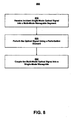
- FIG. 8 is a flowchart 800 of a method for attenuating an optical signal in accordance with one embodiment of the present invention. Although specific steps are disclosed in flowchart 800, such steps are exemplary. That is, embodiments of the present invention are well suited to performing various other steps or variations of the steps recited in flowchart 800. It is appreciated that the steps in flowchart 800 may be performed in an order different than presented, and that not all of the steps in flowchart 800 may be performed.
- an incident single-mode optical signal is received into a multi-mode waveguide, wherein the incident single-mode optical signal is converted to a multi-mode optical signal.
- the multi-mode waveguide has a larger cross-sectional area than the (upstream or input) single-mode waveguide to which it is coupled.
- the multi-mode optical signal is perturbed using a perturbation element.
- the perturbation is disposed either entirely within the multi-mode waveguide, partially inside and partially outside the multi-mode waveguide, or entirely outside the multi-mode waveguide.
- the perturbation element has a three-dimensional refractive index that is different than the refractive index of the multi-mode waveguide.
- the multi-mode optical signal is coupled into a (downstream or output) single-mode waveguide, wherein the multi-mode optical signal is converted to an output single-mode optical signal.
- the single-mode waveguide has a smaller cross-sectional area than the multi-mode waveguide.
- the single-mode output signal is attenuated (e.g., less power) relative to the incident single-mode optical signal.
- the attenuation is achieved by exciting selected modes of the multi-mode optical signal, coupling an amount of optical power associated with the multi-mode optical signal into the selected modes, and coupling the selected modes into the single-mode waveguide.
- the amount of optical power coupled into the selected modes can be changed and controlled. For example, in the case of a liquid-filled trench, the index of refraction can be changed by heating the liquid.
- the embodiments of the present invention utilize a perturbation in a waveguide segment for optical attenuation.
- a single perturbation per waveguide segment is used for optical attenuation.
- the present invention provides an optical attenuator that can be readily integrated into planar lightwave circuits including contemporary silica-based planar lightwave circuits.
- the embodiments of the present invention are particularly suited for optical circuits that couple well with single-mode fibers.
- optical attenuators according to the various embodiments of the present invention can achieve low insertion loss (less than 0.5 dB), have a polarization dependence of less than 0.3 dB for approximately 15 dB attenuation, and have high input power tolerance (less than 25 dBm), with approximately 0.3 dB wavelength uniformity over 1300-1565 nanometers.
Applications Claiming Priority (2)
| Application Number | Priority Date | Filing Date | Title |
|---|---|---|---|
| US10/188,390 US6868222B2 (en) | 2002-07-01 | 2002-07-01 | Optical attenuator using a perturbation element with a multi-mode waveguide |
| US188390 | 2002-07-01 |
Publications (1)
| Publication Number | Publication Date |
|---|---|
| EP1378776A1 true EP1378776A1 (fr) | 2004-01-07 |
Family
ID=29720420
Family Applications (1)
| Application Number | Title | Priority Date | Filing Date |
|---|---|---|---|
| EP03007164A Withdrawn EP1378776A1 (fr) | 2002-07-01 | 2003-03-28 | Atténuateur optique à guide d'onde multimode avec un élément perturbateur |
Country Status (3)
| Country | Link |
|---|---|
| US (1) | US6868222B2 (fr) |
| EP (1) | EP1378776A1 (fr) |
| SG (1) | SG118177A1 (fr) |
Families Citing this family (6)
| Publication number | Priority date | Publication date | Assignee | Title |
|---|---|---|---|---|
| DE10253440A1 (de) * | 2002-11-12 | 2004-05-27 | Infineon Technologies Ag | Planare optische Schaltung |
| JP2005062500A (ja) * | 2003-08-13 | 2005-03-10 | Seikoh Giken Co Ltd | 熱光学型可変光減衰器及びこれを用いたアレイ型可変光減衰器 |
| JP2006251563A (ja) * | 2005-03-11 | 2006-09-21 | Seikoh Giken Co Ltd | 導波路型可変光減衰器 |
| US7693373B2 (en) * | 2007-12-18 | 2010-04-06 | Analog Devices, Inc. | Bidirectional optical link over a single multimode fiber or waveguide |
| KR101165715B1 (ko) * | 2008-12-10 | 2012-07-18 | 한국전자통신연구원 | 광 스위치를 포함하는 광통신 소자 |
| GB2563929A (en) | 2017-06-30 | 2019-01-02 | Oclaro Tech Ltd | Spatial filter |
Citations (4)
| Publication number | Priority date | Publication date | Assignee | Title |
|---|---|---|---|---|
| US5790720A (en) * | 1997-05-06 | 1998-08-04 | Lucent Technologies, Inc. | Acoustic-optic silica optical circuit switch |
| JPH11160634A (ja) * | 1997-09-26 | 1999-06-18 | Hitachi Cable Ltd | 導波路型光スイッチ |
| CA2306325A1 (fr) * | 1999-04-30 | 2000-10-30 | Jds Uniphase Inc. | Coupleur thermo-optique a interference multimode |
| JP2001183710A (ja) * | 1999-12-27 | 2001-07-06 | Kddi Corp | 多モード干渉導波路型光スイッチ |
Family Cites Families (6)
| Publication number | Priority date | Publication date | Assignee | Title |
|---|---|---|---|---|
| US5796906A (en) * | 1996-08-27 | 1998-08-18 | Lucent Technologies Inc. | Optical planar waveguide notch filters |
| US5841913A (en) * | 1997-05-21 | 1998-11-24 | Lucent Technologies Inc. | Acousto-optic planar waveguide modulators |
| US6445843B1 (en) * | 2000-12-20 | 2002-09-03 | Lynx Photonic Networks Inc. | Optical switching system with power balancing |
| US20020018636A1 (en) * | 2000-08-02 | 2002-02-14 | Gemfire Corporation | Device and method for variable attenuation of an optical channel |
| US6546163B2 (en) * | 2000-10-09 | 2003-04-08 | John I. Thackara | Planar waveguide switch and optical cross-connect |
| US7016560B2 (en) * | 2001-02-28 | 2006-03-21 | Lightwave Microsystems Corporation | Microfluidic control for waveguide optical switches, variable attenuators, and other optical devices |
-
2002
- 2002-07-01 US US10/188,390 patent/US6868222B2/en not_active Expired - Fee Related
-
2003
- 2003-03-05 SG SG200301152A patent/SG118177A1/en unknown
- 2003-03-28 EP EP03007164A patent/EP1378776A1/fr not_active Withdrawn
Patent Citations (4)
| Publication number | Priority date | Publication date | Assignee | Title |
|---|---|---|---|---|
| US5790720A (en) * | 1997-05-06 | 1998-08-04 | Lucent Technologies, Inc. | Acoustic-optic silica optical circuit switch |
| JPH11160634A (ja) * | 1997-09-26 | 1999-06-18 | Hitachi Cable Ltd | 導波路型光スイッチ |
| CA2306325A1 (fr) * | 1999-04-30 | 2000-10-30 | Jds Uniphase Inc. | Coupleur thermo-optique a interference multimode |
| JP2001183710A (ja) * | 1999-12-27 | 2001-07-06 | Kddi Corp | 多モード干渉導波路型光スイッチ |
Non-Patent Citations (7)
| Title |
|---|
| BESSE P A ET AL: "THE INTEGRATED PRISM INTERPRETATION OF MULTILEG MACH-ZEHNDER INTERFEROMETERS BASED ON MULTIMODE INTERFERENCE COUPLERS", OPTICAL AND QUANTUM ELECTRONICS, CHAPMAN AND HALL, LONDON, GB, vol. 27, no. 10, 1995, pages 909 - 920, XP000919217, ISSN: 0306-8919 * |
| BOSC D: "Thermo-optical coefficient determination of index liquids used for optimization of optical integrated components", OPTICS COMMUNICATIONS, NORTH-HOLLAND PUBLISHING CO. AMSTERDAM, NL, vol. 194, no. 4-6, 15 July 2001 (2001-07-15), pages 353 - 357, XP004306775, ISSN: 0030-4018 * |
| LEUTHOLD J ET AL: "MULTIMODE INTERFERENCE COUPLERS FOR THE CONVERSION AND COMBINING OFZERO- AND FIRST-ORDER MODES", JOURNAL OF LIGHTWAVE TECHNOLOGY, IEEE. NEW YORK, US, vol. 16, no. 7, 1 July 1998 (1998-07-01), pages 1228 - 1238, XP000778821, ISSN: 0733-8724 * |
| LEUTHOLD J ET AL: "MULTIMODE INTERFERENCE COUPLERS WITH TUNABLE POWER SPLITTING RATIOS", JOURNAL OF LIGHTWAVE TECHNOLOGY, IEEE. NEW YORK, US, vol. 19, no. 5, May 2001 (2001-05-01), pages 700 - 707, XP001154381, ISSN: 0733-8724 * |
| PATENT ABSTRACTS OF JAPAN vol. 1999, no. 11 30 September 1999 (1999-09-30) * |
| PATENT ABSTRACTS OF JAPAN vol. 2000, no. 24 11 May 2001 (2001-05-11) * |
| YAGI M ET AL: "Versatile multimode interference photonic switches with partial index-modulation regions", ELECTRONICS LETTERS, IEE STEVENAGE, GB, vol. 36, no. 6, 16 March 2000 (2000-03-16), pages 533 - 534, XP006014971, ISSN: 0013-5194 * |
Also Published As
| Publication number | Publication date |
|---|---|
| US6868222B2 (en) | 2005-03-15 |
| US20040001687A1 (en) | 2004-01-01 |
| SG118177A1 (en) | 2006-01-27 |
Similar Documents
| Publication | Publication Date | Title |
|---|---|---|
| US6353694B1 (en) | MMI thermo-optic coupler | |
| KR101115735B1 (ko) | 에스오아이 구조체에서의 광의 능동 조작 | |
| JP4768127B2 (ja) | 熱光学ポリマーを含むフォトニックデバイス | |
| US20050207721A1 (en) | Variable optical attenuator | |
| JPWO2006013805A1 (ja) | 平面光回路、波動伝搬回路の設計方法およびコンピュータプログラム | |
| EP1509792A2 (fr) | Composant optique et procede de fabrication associe | |
| US6915029B2 (en) | High density integrated optical chip with low index difference and high index difference waveguide functions | |
| US6707969B2 (en) | Digital thermo-optic switch integrated with variable optical attenuators | |
| US6868222B2 (en) | Optical attenuator using a perturbation element with a multi-mode waveguide | |
| US7006733B2 (en) | Method and apparatus for channel selective control of light propagation in an optical waveguide | |
| KR20020026774A (ko) | 외부 조절이 가능한 광도파로형 고차모드 발생기 | |
| US6668107B2 (en) | Method and apparatus for reducing optical insertion loss in planar lightwave circuits through dielectric perturbation optimization | |
| JPWO2016051698A1 (ja) | リブ型光導波路およびそれを用いた光合分波器 | |
| US20030016937A1 (en) | Variable optic attenuator by waveguide bend loss | |
| JP4383815B2 (ja) | ホログラフィック波動伝達媒体の製造方法 | |
| JP2004055717A (ja) | 可変光利得制御器 | |
| KR100281552B1 (ko) | 열광학 효과를 이용한 집적광학형 가변 광감쇄기 | |
| WO1993020476A1 (fr) | Dispositifs photoniques utilisant des guides d'ondes optiques induits par des solitons spatiaux sombres | |
| JP2008281639A (ja) | 光偏向素子、光偏向モジュール及び光スイッチモジュール、並びに光偏向方法 | |
| KR101423978B1 (ko) | 열광학 가변 광감쇄기 | |
| Yen et al. | Silicon photonics multi-channel Bragg reflectors based on narrowband cladding-modulated gratings | |
| JP4113161B2 (ja) | 光導波路型スイッチ | |
| KR100237187B1 (ko) | 편광 독립 가변 광 감쇄기 | |
| Masuda et al. | Beam steering type 1: 4 optical switch with polymer thermo-optic phase shifters in a silica arrayed-waveguide | |
| Ishida et al. | Planar 1 x 2 optical prism deflector switch fabricated on a silica waveguide |
Legal Events
| Date | Code | Title | Description |
|---|---|---|---|
| PUAI | Public reference made under article 153(3) epc to a published international application that has entered the european phase |
Free format text: ORIGINAL CODE: 0009012 |
|
| AK | Designated contracting states |
Kind code of ref document: A1 Designated state(s): AT BE BG CH CY CZ DE DK EE ES FI FR GB GR HU IE IT LI LU MC NL PT RO SE SI SK TR |
|
| AX | Request for extension of the european patent |
Extension state: AL LT LV MK |
|
| 17P | Request for examination filed |
Effective date: 20040609 |
|
| 17Q | First examination report despatched |
Effective date: 20040714 |
|
| AKX | Designation fees paid |
Designated state(s): DE FR GB |
|
| STAA | Information on the status of an ep patent application or granted ep patent |
Free format text: STATUS: THE APPLICATION IS DEEMED TO BE WITHDRAWN |
|
| 18D | Application deemed to be withdrawn |
Effective date: 20041125 |