TECHNICAL FIELD
-
Embodiments of the present invention relate to the field of optical
circuits. More specifically, embodiments of the present invention relate to
optical attenuators.
BACKGROUND ART
-
A class of optical circuits includes circuits known as planar lightwave
circuits (PLCs). In such circuits, optical signals received from input terminals
are selected, redirected and transmitted to output terminals. Often, the
redirection is performed using an array of switches.
-
In fully optical circuits, optical signals are carried along waveguides.
Waveguides are typically formed as a doped core region situated within a
substrate. The doped core region and the surrounding substrate generally
have different refractive indexes. An optical signal is guided through the
substrate along the waveguide. Perturbations may be formed within or along
the waveguide to perform switching operations on the optical signals traveling
in the waveguide, for example. Typically, the waveguides are laid out as a
grid having intersections, or cross points, and the perturbations are formed at
the intersections.
-
A perturbation can be a liquid-filled trench used as an optical switch, a
doped portion of the waveguide, or some other structure or material having a
refractive index different than the refractive index of the waveguide. The
refractive index of a switching perturbation is capable of being changed
between a number of possible states, for instance, between two levels. One of
the levels causes the optical signals to pass through the perturbation without
changing direction, and the other level causes the optical signals to change
direction and pass into an intersecting waveguide. In the case of a liquid-filled
trench, the liquid may be moved aside in some manner to leave a gaseous
phase at the intersection; for example, a bubble may be formed in the trench by
heating the liquid. In general, the perturbation defines a three-dimensional
index of refraction distribution, positioned at an intersection of two waveguides;
changing the value of the refractive index performs a switching operation.
-
Prior Art Figure 1 illustrates an exemplary switching device 10 that is
able to switch M input optical paths (designated Input-1 11, Input-2 13, ...,
Input-M 15) into N output optical paths (designated Output-1 17, Output-2 19,
..., Output-N 21). The input and output paths can be waveguide segments;
however, although described herein as such, in general the optical paths can
be any optical path capable of conducting an optical signal. Device 10
includes optical switches (designated Si,j, where i is the input row and j is the
output column) at each waveguide intersection. Prior Art Figure 1 illustrates
two of the possible optical paths through device 10. The first path, designated
by vectors 12a and 12b, shows an input signal Input-1 11 directed via switch
S1,2 to the output terminal Output-2 19. The second path, designated by
vectors 14a and 14b, shows an input signal Input-2 directed via switch S2,N to
the output terminal Output-N 21.
-
Prior Art Figure 2 illustrates a view of section 18 of device 10. Section
18 includes a fluid optical switch S2,2 having a trench 22. Switch S2,2 is
defined by trench 22 formed between a break in waveguide 24 and other
layers of device 10 including, without limitation, cladding layers 26 and
heating circuit layer 28, including heating element 29. The layers of device 10
are typically built on a substrate 30. Such switches are known in the art.
-
A variation in optical power within an optical circuit may cause
deleterious effects, including detector saturation and inter-channel cross-talk,
that can lead to transmission errors. Because power fluctuations occur
dynamically within an optical circuit, it Is of interest to have a means of
adjustment. This is the function of variable optical attenuators (VOAs).
-
The VOAs of the prior art each have their disadvantages. Prior art
VOAs may be too large, too expensive, or require too much power. Prior art
VOAs may also have a slow response or a high insertion loss. In addition,
prior art VOAs may not be readily integrated with optical circuits and switches
such as those described above. Accordingly, there is a continuing need for
VOAs that provide an improvement over the disadvantages of the prior art.
DISCLOSURE OF THE INVENTION
-
Embodiments of the present invention pertain to an optical attenuator
having a multi-mode waveguide segment and a perturbation element. An
incident single-mode optical signal is converted to a multi-mode optical signal
in the multi-mode waveguide segment. The optical attenuator couples
incident light into higher order modes of the multi-mode waveguide segment
resulting in attenuation of the incident optical signal.
BRIEF DESCRIPTION OF THE DRAWINGS
-
The accompanying drawings, which are incorporated in and form a part
of this specification, illustrate embodiments of the invention and, together with
the description, serve to explain the principles of the invention. The drawings
referred to in this description should not be understood as being drawn to
scale except if specifically noted.
- PRIOR ART FIGURE 1 illustrates a prior art optical switching device.
- PRIOR ART FIGURE 2 illustrates a portion of the prior art switching
device of Figure 1.
- FIGURE 3 illustrates a model of a perturbation acting on an optical
signal in accordance with one embodiment of the present invention.
- FIGURE 4 illustrates a perturbation across a waveguide according to
one embodiment of the present invention.
- FIGURES 5A, 5B and 5C illustrate embodiments of an optical
attenuator according to embodiments of the present invention.
- FIGURE 6 illustrates an optical attenuator in operation according to one
embodiment of the present invention.
- FIGURE 7 illustrates an optical device including optical attenuators
according to one embodiment of the present invention.
- FIGURE 8 is a flowchart of a method for attenuating an optical signal In
accordance with one embodiment of the present invention.
-
DETAILED DESCRIPTION OF THE INVENTION
-
Reference will now be made in detail to the various embodiments of the
invention, examples of which are illustrated in the accompanying drawings.
While the invention will be described in conjunction with these embodiments,
it will be understood that they are not intended to limit the invention to these
embodiments. On the contrary, the invention is intended to cover alternatives,
modifications and equivalents, which may be included within the spirit and
scope of the invention as defined by the appended claims. Furthermore, in
the following detailed description of the present invention, numerous specific
details are set forth in order to provide a thorough understanding of the
present invention. In other instances, well known methods, procedures,
components, and circuits have not been described in detail as not to
unnecessarily obscure aspects of the present invention.
-
Embodiments of the present invention pertain to optical attenuators that
can be readily Integrated into planar lightwave circuits (PLCs) including
contemporary silica-based PLCs and in particular silica-based PLCs that
match (mate) with single-mode fibers. In general, the optical attenuators of the
present invention function to attenuate an aspect (e.g., power) of an optical
signal transmitted using an optical waveguide.
-
An optical waveguide can transmit optical signals, or light, in both
guided and unguided modes. In the guided mode, light propagates down a
waveguide via total internal reflection and has a substantial fraction of its
power confined within the waveguide. In the unguided mode, power is lost as
light propagates away from the guiding layer; the unguided light does not
propagate a significant distance along its direction of travel.
-
In designing a system with guided wave optics, it may be desirable to
use only the lowest order guided mode present. The lowest order guided
mode has the largest fraction of the power of the optical signal localized within
the waveguide core. This can minimize dispersion and loss associated with
the presence of higher order modes. The feasibility of such single mode
structures has been demonstrated.
-
If light traveling within a waveguide is confined to a particular guided
mode, it remains In that mode as long as it is traveling in a perturbation-free
environment. In many optical devices, including a variety of PLCs such as
optical switches, structures such as trenches are often used at the intersection,
or cross point, of two waveguides to perform a switching operation in an
optical switch. Such a structure introduces a perturbation in the path of the
optical signal. Perturbations can create a variation in the dielectric constant in
the region of the perturbation. On encountering a variation in the dielectric
constant, the optical signal behaves differently.
-
Light propagating near a dielectric perturbation can be thought of as
being comprised of a number of modes. A description of the light at a
dielectric perturbation includes a sum over all of the possible modes including
a finite number of possible guided modes and an infinite number of radiation,
or continuum, modes. Dielectric constants, geometry, and symmetry of the
perturbation determine which modes are present as well as their relative
proportions. Consequently, a perturbation in the dielectric constant can
couple modes and allow an exchange of energy from one mode to higher
order modes.
-
A perturbation can cause an optical signal to lose some of its power
due to diffraction and radiation. Mode conversion and coupling can be a
source of loss. Radiation modes excited near an obstacle such as a trench or
other type of perturbation may not be re-trapped and guided into the
waveguide on the other side of the perturbation, thereby losing power. The
magnitude of such a loss depends on the nature of the dielectric perturbation,
Δε, which in turn depends on the refractive index distribution, Δn, as well as
the geometry and symmetry of the structure. In accordance with the various
embodiments of the present invention, perturbations in the dielectric constant
are designed that can attenuate optical signals and minimize insertion loss.
-
In general, light traversing a perturbation 50 (illustrated as a trench 50)
in Figure 3 will diffract and scatter from the obstacle as shown by vectors 51.
Light originating from the input waveguide 54 that scatters from the
perturbation may not lie within the numerical aperture of output waveguide 56,
thus realizing optical loss. Optical loss may also occur from diffraction; the
spreading out of the light as it crosses trench 50 leads to a larger size, and
thus poorly mode-matched, beam of light at the output waveguide 56.
Excitation of higher order "leaky" modes can lead to additional optical loss.
The trench refractive index distribution, geometry, and symmetry can be
optimized to prevent the excitation of these higher order modes.
-
Figure 4 illustrates a perturbation 62 across a waveguide 64 according
to one embodiment of the present invention. For the perturbation 62
illustrated in Figure 4, the dominant mode component 68 and the higher-order
mode components 70 of the optical signal combine in superposition to form a
wavefront 72. The trench geometry and refractive index distribution are
selected so that the phases and amplitudes of the dominant mode and any
higher order modes excited by the perturbation 62 are adjusted appropriately
to allow recapture within the coupling length of the output waveguide.
-
In general, mode coupling is a more complicated function depending
on the propagation constants of the excited modes as well as the geometry
and refractive index distribution of the perturbation. Additionally, a waveguide
perturbation can lead to the excitation of lossy higher order modes. This is the
physical mechanism for attenuation.
-
Suppose, for example, that light is incident on a dielectric perturbation
such as a trench. The representation of the light near the trench is a sum over
an infinite number of modes as follows:
-
Note that symbols used herein but not specifically described have the
usual and conventional meaning within the art.
-
The coefficients aj (z) in equation (1) determine how much of each
mode is present and are themselves determined by the specific details of the
perturbation. That these coefficients depend on distance illustrates how
different mixtures of modes can exist as a function of position along the
waveguide. The coefficients a +£ / j(z) represent waves traveling in the original
propagation direction, while the a -£ / j(z) are reflected waves generated by the
obstacle. There are two types of modes present in the formula: guided modes
and radiation modes. The discrete sum includes guided modes while the
integral is a sum over the infinite number of radiation modes. Thus, a careful
through-loss optimization focuses on understanding the continuum of
radiation modes and learning how to subtly adjust their phases and decay
lengths to ensure optimal re-coupling.
-
For clarity of exposition, and without loss of generality, it is possible to
drop the radiation modes from equation (1) (for example, by employing a
suitable and well-known discretization procedure) and consider the electric
field as a sum of discrete modes only. By assuming that amplitudes vary
slowly with position (slowly varying amplitude approximation) and by using
the orthogonality property of the transverse electric modes, a differential
equation -- the so-called coupled mode equation -- is derived for the
amplitudes:
where P
pert represents the interaction of incident light with a perturbed
dielectric constant.
-
Equation (2) shows that the coupling into mode
j depends on the
overlap integral of the mode
j multiplied by the perturbation. If the Incident
light is contained in mode
m, then:
and thus the perturbation takes the form:
-
The perturbation is seen to couple mode m into mode j via the overlap
integral.
-
Several interesting features can be derived from equation (3). First, in
the limit of a very weak perturbation, PPert (x,z,t) ≈ 0, there is no coupling
between modes. Instances of no coupling can occur when the overlap
integral vanishes, such as in special occasions where the perturbation has a
high degree of symmetry. For example, a symmetric notch in a slab
waveguide can only couple the lowest order mode to a higher order mode
with even symmetry. Another result found by analyzing the overlap integral is
that power can oscillate back and forth between modes as a function of the
length of the obstacle. The coupling in this case is often enhanced when the
perturbation makes up the difference, Δβ, between the propagation constants
of the modes in question. In practice this occurs when the length L of the
perturbation is of order Δβ ≈ const/L. In a similar fashion, a periodic
perturbation, with spacing Λ, can couple modes. In this case, a particular
spatial Fourier component of the perturbation causes coupling when Δβ ≈ 1/Λ.
Mode coupling via the spacing of the perturbations may contribute to optical
loss.
-
Figure 5A illustrates one embodiment of an optical attenuator 500a
according to the present invention. In general, an optical attenuator functions
to attenuate an aspect (e.g., power) of an optical signal. One use of an optical
attenuator, or variable optical attenuator (VOA), is for gain stabilization. An
optical amplifier, such as an erbium-doped fiber amplifier (EDFA), operates in
saturation with a constant total output power. Thus, if the number of single
channel inputs to the amplifier change, an individual output channel can see a
rapid variation in power. According to its various embodiments, the present
invention can be a real-time means of adjustment of optical power. Another
use of a VOA described by the various embodiments of the present invention
is to flatten the gain of an amplifier or to provide spectral equalization of a
dense wavelength division multiplexing (DWDM) signal. For example, a VOA
may be placed on each of the output channels of an arrayed waveguide
grating (AWG) demultiplexer to control the amplitude of individual optical
channels of differing wavelengths. A VOA as described according to the
various embodiments of the present invention can be used for cross-talk
reduction in an optical switch. For example, a VOA placed in the off-state arm
of an optical switch can be used to remove any stray light leaked from the on-state
path. A VOA can also be employed within an optical switch to equalize
the insertion loss between different paths.
-
With reference to Figure 5A, in the present embodiment, a perturbation
510 is situated across multi-mode waveguide segment 520, such that
perturbation 510 is disposed partially outside of multi-mode waveguide
segment 520. Multi-mode waveguide segment 520 has a three-dimensional
refractive index distribution ncore, while the surrounding substrate has a
refractive index distribution nsubstrate. Typically, perturbation 510 has a
refractive index distribution npert that is different from ncore. In general,
perturbation 510 may be comprised of a number of different materials, with the
purpose of effecting a change in the index of refraction of multi-mode
waveguide segment 520. In addition to the three-dimensional refractive index
distribution, the symmetry of the perturbation is an important consideration in
determining the mode coupling.
-
In one embodiment, perturbation 510 is a dielectric perturbation that
includes a liquid-filled trench including (or neighboring) a heater element. In
this embodiment, the variation of the liquid's refractive index with temperature
is typically on the order of -10-4/°C. Typically, refractive index changes of a few
parts in a thousand are sufficient to provide large coupling constants with
appropriate engineering of the perturbation. In another embodiment,
perturbation 510 includes a hybrid material with the proper electro-optic,
thermo-optic or elastic properties, such as a nonlinear optical crystal or
polymer.
-
Multi-mode waveguide segment 520 is coupled between single- mode
waveguide segments 530a and 530b. In one embodiment, multi-mode
waveguide segment 520 has a larger cross-sectional area (e.g., diameter)
than single- mode waveguides 530a and 530b. In this embodiment, the
coupling of single-mode waveguide segment 530a to multi-mode segment
520 is essentially adiabatic, resulting in low energy loss between these two
segments. Although the input and output paths are described herein as
waveguide segments, in general the optical paths can be any optical path
capable of conducting an optical signal.
-
The perturbation 510 forms some angle measurable from a reference.
In this case, the reference is a line orthogonal to multi-mode waveguide
segment 520. The angle may be any value ranging from zero degrees to
360 degrees. Based on empirical data, a numerical solution or the like, a
particular value of can be determined that will provide a desired amount of
optical attenuation. Also, the value of can be selected to minimize insertion
loss (including back reflection effects) while still achieving a desired amount of
attenuation.
-
Figures 5B and 5C illustrate alternate embodiments of an optical
attenuator according to the present invention. Optical attenuator 500b of
Figure 5B shows a perturbation 540 entirely within multi-mode waveguide
segment 520. Optical attenuator 500c of Figure 5C shows a perturbation 550
entirely outside of multi-mode waveguide segment 520. In general, a
perturbation (e.g., 500a, 500b, and 500c) may be situated relative to multi-mode
waveguide segment 520, in a position to cause perturbation of a multi-mode
optical signal being guided along multi-mode waveguide segment 520.
-
Also, with regard to Figures 5A-5C, perturbations 510, 540 and 550 are
illustrated as being square or rectangular in shape. However, it is understood
that perturbations are not limited to such shapes and that, in the three-dimensional
world, perturbations may be shaped in a variety of different ways
to achieve a desired amount of optical attenuation, perhaps with consideration
also to a desired amount of insertion loss. In addition, the shape of the
coupling between the single-mode and multi-mode waveguides, generally
illustrated as tapering, may be shaped in different ways depending on a
desired amount of optical attenuation and perhaps depending on a desired
amount of insertion loss. However, in one embodiment, the coupling of the
single-mode waveguide segment 530a to the multi-mode segment 520 is
essentially adiabatic, as mentioned above.
-
Figure 6 illustrates an optical attenuator 500a in operation according to
one embodiment of the present invention. Although described in the context
of optical attenuator 500a of Figure 5A, it is appreciated that the description is
also applicable to the optical attenuators embodied by Figures 5B and 5C.
-
With reference to Figure 6, incident light from single-mode waveguide
530a is coupled into a larger diameter multi-mode waveguide 520. The multi-mode
waveguide 520 is engineered to support higher order modes at the
operating wavelength. These higher order modes are excited by a suitable
(dielectric) perturbation 510. Changing the refractive index distribution of the
perturbation 510 couples a variable amount of the incident optical power into
the excited modes. Attenuation results from the fact that light in a high order
mode does not couple efficiently into the output single-mode waveguide 530b.
-
As described above, a description of the light at a dielectric perturbation
includes a sum over all of the possible modes including a finite number of
possible guided modes and an infinite number of radiation, or continuum,
modes. Dielectric constants, geometry, and symmetry of the perturbation
determine which modes are present as well as their relative proportions.
Consequently, a perturbation (e.g., perturbation 510) in the dielectric constant
can couple modes and allow an exchange of energy from one mode to higher
order modes. Mode conversion and coupling can be a source of loss.
Radiation modes excited near an obstacle such as a trench or other type of
perturbation may not be re-trapped and guided into the waveguide on the
other side of the perturbation, thereby losing power. The magnitude of such a
loss depends on the nature of the dielectric perturbation, Δε, which in turn
depends on the refractive index distribution, Δn, as well as the geometry and
symmetry of the structure. The geometry and refractive index distribution of
perturbation 510 can be selected so that the phases of the dominant mode
and any higher order modes excited by perturbation 510 are adjusted
appropriately to allow recapture within the coupling length of the output
waveguide (e.g., single-mode waveguide 530b).
-
Figure 7 illustrates an optical device 700 including optical attenuators
according to one embodiment of the present invention. In one embodiment,
optical device 700 is a planar waveguide circuit (PLC). An advantage of the
present invention, in its various embodiments, is that it can be readily
integrated within a planar lightwave circuit.
-
In the present embodiment, optical device 700 includes an array of
waveguides including input optical signal paths 11, 13, and 15 (representing
inputs 1 to M) and output signal paths 17, 19, and 21 (representing outputs 1
to N) forming a grid of M rows by N columns with M times N intersections, or
cross points. The input and output paths can be waveguide segments. While
described herein as waveguide segments, the optical paths can be any
optical paths capable of conducting an optical signal, for example, optical
fiber.
-
While illustrated as single lines, input waveguides 11, 13, and 15 and
output waveguides 17, 19, and 21 typically actually include cores or channels
supported by a substrate, cladding, or both, through which light travels. Each
waveguide has a three-dimensional refractive index distribution -- waveguide
refractive index distribution -- for guiding light.
-
To perform a switching function, the optical device 700 includes an
array of individual optical switches, one switch located at each intersection.
and designated Si,j, where i is the input path and the j is the output path the
switch is connected. The switches are transmissive, in that when filled with an
index matching medium, such as a liquid having a refractive index the same
as or similar to the refractive index of the waveguide segments (of the input
and output paths), the switches allow light traveling in the waveguide to pass
directly through. When devoid of the index matching medium, such as when
the switch (a trench) is filled with a gas or bubble (for example, upon heating),
the incident light is reflected Into an adjoining waveguide, Instead of being
transmitted through the switch. The switches Si,j can be considered active
perturbations that operate on the optical signals that are passing through.
-
While illustrated as a matrix of three (3) rows and three (3) columns for
a total of nine optical switch points, the optical device 700 may include any
number of input waveguides and output waveguides, having a commensurate
number of cross point switches at the intersections thereof. Furthermore,
while illustrated as intersecting at right angles, the input waveguides and the
output waveguides can intersect at angles other than right angles. For
example, the optical device 700 may be an optical switch matrix having a 32-by-32
matrix having 32 input waveguides and 32 output waveguides, or it may
be even larger. For simplicity, a 3-by-3 optical switch matrix is illustrated
herein. Furthermore, in the present embodiment of optical device 700, each of
the input paths (11, 13, and 15) and the output paths (17, 19, and 21) crosses
multiple switch elements Si,j at trenches, thus resulting in each input
waveguide and each output waveguide being comprised of a plurality of
waveguide segments. In use, the waveguide segments can be connected to
optical fibers at the inputs and outputs. For example, the input waveguides
11, 13 and 15 and the output waveguides 17, 19 and 21 can be connected to
optical fiber ribbon cables using V-groove arrays, the waveguides being
typically spaced on the order of 0.25 millimeters apart. Here, the switches Si,j
are active perturbations for operating on the optical signal.
-
In the present embodiment, optical device 700 (e.g., a planar lightwave
circuit) includes a number of optical attenuator perturbations exemplified by
perturbations 710, 711, 712, 713 and 714. For simplicity of illustration, only
these perturbations are illustrated; however, it is appreciated that optical
device 700 may include any number of perturbations for optical attenuation.
In one embodiment, only a single perturbation is used per waveguide
segment for optical attenuation; that is, for example, only a single perturbation
710 may be used between switches S1,2 and S1,N. In another embodiment,
more than one perturbation may be used per waveguide segment.
-
Perturbations 710-714 are shown as being between the switches Si,j;
however, under some circumstances, such perturbations may be located at
the intersections of waveguides. That is to say, in some instances, the
switches Si,j may also be used for optical attenuation. Also, although the
perturbations are illustrated as being placed roughly at the midpoint between
switches, it is understood that they may be placed at any location between
switches.
-
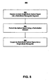
Figure 8 is a flowchart 800 of a method for attenuating an optical signal
in accordance with one embodiment of the present invention. Although
specific steps are disclosed in flowchart 800, such steps are exemplary. That
is, embodiments of the present invention are well suited to performing various
other steps or variations of the steps recited in flowchart 800. It is appreciated
that the steps in flowchart 800 may be performed in an order different than
presented, and that not all of the steps in flowchart 800 may be performed.
-
In step 810, in the present embodiment, an incident single-mode optical
signal is received into a multi-mode waveguide, wherein the incident single-mode
optical signal is converted to a multi-mode optical signal. In one
embodiment, the multi-mode waveguide has a larger cross-sectional area
than the (upstream or input) single-mode waveguide to which it is coupled.
-
In step 820, in the present embodiment, the multi-mode optical signal is
perturbed using a perturbation element. In various embodiments, the
perturbation is disposed either entirely within the multi-mode waveguide,
partially inside and partially outside the multi-mode waveguide, or entirely
outside the multi-mode waveguide. In one embodiment, the perturbation
element has a three-dimensional refractive index that is different than the
refractive index of the multi-mode waveguide.
-
In step 830, in the present embodiment, the multi-mode optical signal is
coupled into a (downstream or output) single-mode waveguide, wherein the
multi-mode optical signal is converted to an output single-mode optical signal.
In one embodiment, the single-mode waveguide has a smaller cross-sectional
area than the multi-mode waveguide. The single-mode output signal is
attenuated (e.g., less power) relative to the incident single-mode optical
signal. In one embodiment, the attenuation is achieved by exciting selected
modes of the multi-mode optical signal, coupling an amount of optical power
associated with the multi-mode optical signal into the selected modes, and
coupling the selected modes into the single-mode waveguide. In one
embodiment, by changing the refractive index, the amount of optical power
coupled into the selected modes can be changed and controlled. For
example, in the case of a liquid-filled trench, the index of refraction can be
changed by heating the liquid.
-
In summary, the embodiments of the present invention utilize a
perturbation in a waveguide segment for optical attenuation. In one
embodiment, a single perturbation per waveguide segment is used for optical
attenuation. In its various embodiments, the present invention provides an
optical attenuator that can be readily integrated into planar lightwave circuits
including contemporary silica-based planar lightwave circuits. The
embodiments of the present invention are particularly suited for optical circuits
that couple well with single-mode fibers. In addition, optical attenuators
according to the various embodiments of the present invention can achieve
low insertion loss (less than 0.5 dB), have a polarization dependence of less
than 0.3 dB for approximately 15 dB attenuation, and have high input power
tolerance (less than 25 dBm), with approximately 0.3 dB wavelength
uniformity over 1300-1565 nanometers.
-
The present invention is thus described in various embodiments. While
the present invention has been described in particular embodiments, it should
be appreciated that the present invention should not be construed as limited
by such embodiments, but rather construed according to the following claims.