EP1376743B1 - Hocheffizienter Tiefpassfilter - Google Patents
Hocheffizienter Tiefpassfilter Download PDFInfo
- Publication number
- EP1376743B1 EP1376743B1 EP03013321A EP03013321A EP1376743B1 EP 1376743 B1 EP1376743 B1 EP 1376743B1 EP 03013321 A EP03013321 A EP 03013321A EP 03013321 A EP03013321 A EP 03013321A EP 1376743 B1 EP1376743 B1 EP 1376743B1
- Authority
- EP
- European Patent Office
- Prior art keywords
- line
- region
- substrate
- circuit
- port line
- Prior art date
- Legal status (The legal status is an assumption and is not a legal conclusion. Google has not performed a legal analysis and makes no representation as to the accuracy of the status listed.)
- Expired - Lifetime
Links
Images
Classifications
-
- H—ELECTRICITY
- H01—ELECTRIC ELEMENTS
- H01P—WAVEGUIDES; RESONATORS, LINES, OR OTHER DEVICES OF THE WAVEGUIDE TYPE
- H01P1/00—Auxiliary devices
- H01P1/20—Frequency-selective devices, e.g. filters
- H01P1/201—Filters for transverse electromagnetic waves
- H01P1/203—Strip line filters
- H01P1/2039—Galvanic coupling between Input/Output
-
- H—ELECTRICITY
- H05—ELECTRIC TECHNIQUES NOT OTHERWISE PROVIDED FOR
- H05K—PRINTED CIRCUITS; CASINGS OR CONSTRUCTIONAL DETAILS OF ELECTRIC APPARATUS; MANUFACTURE OF ASSEMBLAGES OF ELECTRICAL COMPONENTS
- H05K1/00—Printed circuits
- H05K1/02—Details
- H05K1/0213—Electrical arrangements not otherwise provided for
- H05K1/0237—High frequency adaptations
- H05K1/024—Dielectric details, e.g. changing the dielectric material around a transmission line
-
- H—ELECTRICITY
- H05—ELECTRIC TECHNIQUES NOT OTHERWISE PROVIDED FOR
- H05K—PRINTED CIRCUITS; CASINGS OR CONSTRUCTIONAL DETAILS OF ELECTRIC APPARATUS; MANUFACTURE OF ASSEMBLAGES OF ELECTRICAL COMPONENTS
- H05K1/00—Printed circuits
- H05K1/16—Printed circuits incorporating printed electric components, e.g. printed resistors, capacitors or inductors
- H05K1/165—Printed circuits incorporating printed electric components, e.g. printed resistors, capacitors or inductors incorporating printed inductors
Definitions
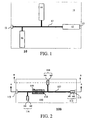
- a short-circuited line acts as a pure inductance at 1/8 wavelength long, acts as a parallel LC impedance at 1/4 wavelength long, acts a pure capacitance at 3/8 wavelengths long, and acts like a series LC circuit at 1/2 wavelength long. This cycle repeats every half wavelength with smooth transitions between each of the above mentioned points.
- properly chosen single port resonant line segments may be used as parallel-resonant, series-resonant, inductive, or capacitive circuits.
- Single port resonant lines are commonly manufactured on specially designed printed circuit boards.
- the resonant lines can be formed many different ways. Three common implementations are described below.
- One configuration known as microstrip places the resonant line on a board surface and provides a second conductive layer coupled to the board. This second conductive layer is commonly referred to as a ground plane.
- a second type of configuration known as buried microstrip is similar except that the resonant line is covered with a dielectric substrate material.
- stripline the resonant line is sandwiched between two electrically conductive (ground) planes, which can be proximate to the board or coupled to the board.
- coupled to the board means attached to the surface of the board or contained within the board.
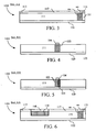
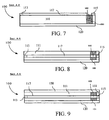
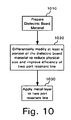
- Responses of a substrate layer to a given energetic stimuli may be substantially permanent in whole or in part. Permanent responses permit one time application of an appropriate stimulus to achieve one or more desired physical substrate layer properties. Physical properties may also be dynamically controlled, such as through the use of discharge electrodes which can permit application of a time-varying electrical field across the substrate layer. Dynamic control of the substrate layer properties, such as the permittivity, can be used to control the susbstrate layer physical characteristics to optimize the performance of the resonant line in response to varying signal characteristics, for example a substantial change in operating frequency.
Landscapes
- Physics & Mathematics (AREA)
- Electromagnetism (AREA)
- Control Of Motors That Do Not Use Commutators (AREA)
- Fats And Perfumes (AREA)
- Piezo-Electric Or Mechanical Vibrators, Or Delay Or Filter Circuits (AREA)
Claims (5)
- Schaltung zum Verarbeiten von Funkfrequenzsignalen, aufweisend:ein Substrat (110) einschließlich zumindest einer dielektrischen Schicht (110), wobei die dielektrische Schicht (110) zumindest einen ersten Bereich (111) und zumindest einen zweiten Bereich (101, 103, 105) aufweist, die unterschiedlich modifiziert sind, um eine unterschiedliche Permeabilität und / oder eine unterschiedliche Permittivität aufzuweisen;zumindest eine Masse (120), die an dem Substrat (110) befestigt ist; undein Leitung (100) mit zwei Anschlüssen, mit zumindest einem Teil der Leitung (100) mit zwei Anschlüssen am ersten Bereich (111) befestigt und mit zumindest einem Teil der Leitung (100) mit zwei Anschlüssen am zweiten Bereich (101, 103, 105) befestigt, wobei die Leitung (100) mit zwei Anschlüssen eine Resonanzleitung (102) umfasst;dadurch gekennzeichnet, dass
eine unterschiedliche Modifikation erreicht wird durch wahlweise Verwendung mindestens eines Metamaterials, das umfasst:ferritische organokeramische Teilchen oder organokeramische Niob-Teilchen oderorganofunktionalisierte keramische Verbundteilchen, die aufweisen können:das Metamaterial ein Verbundstoff ist, der durch das Mischen oder eine Anordnung zweier oder mehrerer Materialien auf einer molekularen oder Nanometer-Ebene gebildet wird.Metalloxide, einschließlich Aluminiumoxid, Kalziumoxid, Magnesiumoxid, Nickeloxid, Zirkonoxid und Niob (II, IV und V)-Oxid, Lithiumniobat, undZirkonate, einschließlich Kalziumzirkonat und Magnesiumzirkonat, undferritdotiertes Kalziumtitanat unter Verwendung von Magnesium, Strontium oder Niob als Dotiermetallen, undferrit- oder niob-dotiertes Kalzium oder Bariumtitanatzirkonate, und wobei - Schaltung nach Anspruch 1, wobei der zweite Bereich (101, 103, 105) eine Vielzahl entsprechender Teile (101, 103, 105) umfasst und wobei die Leitung (100) mit zwei Anschlüssen ein Tiefpassfilter ist, wobei der Tiefpassfilter einen Wandlerleitungsabschnitt (112) auf zumindest einem Teil des ersten Bereichs (111) und auf zumindest einem entsprechenden Teil (101) des zweiten Bereichs (101, 103, 105) umfasst, und zumindest einen ersten Stichleitungsabschnitt (114) auf zumindest einem Teil des ersten Bereichs (111) auf zumindest einem entsprechenden Teil (103) des zweiten Bereichs (101, 103, 105) umfasst.
- Schaltung nach Anspruch 1 oder 2, wobei der erste Bereich (111) und der zweite Bereich (101, 103, 105) der dielektrischen Schicht (110) unterschiedlich modifiziert sind, um eine Kapazität zwischen der Leitung (100) mit zwei Anschlüssen und einer Masseplatte (102) anzupassen.
- Schaltung nach einem der vorhergehenden Ansprüche, wobei der erste Bereich (111) und der zweite Bereich (101, 103, 105) der dielektrischen Schicht (110) unterschiedlich modifiziert sind, um einen Gütefaktor der Leitung (100) mit zwei Anschlüssen anzupassen.
- Schaltung nach Anspruch 1, wobei die Leitung (100) mit zwei Anschlüssen eine Vielzahl von Stichleitungsabschnitten (112, 114, 116) aufweist und jeder aus der Vielzahl der Stichleitungsabschnitte (112, 114, 116) mit seinem eigenen entsprechenden zweiten Substratbereich (101, 103, 105) gekoppelt ist.
Applications Claiming Priority (2)
| Application Number | Priority Date | Filing Date | Title |
|---|---|---|---|
| US185187 | 1988-04-22 | ||
| US10/185,187 US6794952B2 (en) | 2002-06-27 | 2002-06-27 | High efficiency low pass filter |
Publications (2)
| Publication Number | Publication Date |
|---|---|
| EP1376743A1 EP1376743A1 (de) | 2004-01-02 |
| EP1376743B1 true EP1376743B1 (de) | 2006-08-23 |
Family
ID=29717990
Family Applications (1)
| Application Number | Title | Priority Date | Filing Date |
|---|---|---|---|
| EP03013321A Expired - Lifetime EP1376743B1 (de) | 2002-06-27 | 2003-06-12 | Hocheffizienter Tiefpassfilter |
Country Status (7)
| Country | Link |
|---|---|
| US (1) | US6794952B2 (de) |
| EP (1) | EP1376743B1 (de) |
| JP (1) | JP2004032768A (de) |
| AT (1) | ATE337619T1 (de) |
| AU (1) | AU2003204880A1 (de) |
| CA (1) | CA2432183C (de) |
| DE (1) | DE60307730T2 (de) |
Cited By (1)
| Publication number | Priority date | Publication date | Assignee | Title |
|---|---|---|---|---|
| WO2009067197A3 (en) * | 2007-11-16 | 2009-09-11 | Rayspan Corporation | Filter design methods and filters based on metamaterial structures |
Families Citing this family (9)
| Publication number | Priority date | Publication date | Assignee | Title |
|---|---|---|---|---|
| EP2933225A1 (de) * | 2004-07-23 | 2015-10-21 | The Regents of The University of California | Metamaterialien |
| JP4638711B2 (ja) | 2004-10-27 | 2011-02-23 | 株式会社エヌ・ティ・ティ・ドコモ | 共振器 |
| JP4628991B2 (ja) * | 2006-05-10 | 2011-02-09 | 富士通コンポーネント株式会社 | 分布定数型フィルタ装置 |
| KR101066548B1 (ko) | 2008-11-19 | 2011-09-21 | 한국전자통신연구원 | 저역 통과 여파기와 그 설계 방법 |
| US8334734B2 (en) | 2009-08-25 | 2012-12-18 | Hollinworth Fund, L.L.C. | Printed multilayer filter methods and designs using extended CRLH (E-CRLH) |
| JP6169395B2 (ja) | 2012-08-27 | 2017-07-26 | 株式会社トーキン | 共振器 |
| KR101556307B1 (ko) | 2014-06-10 | 2015-10-02 | 경북대학교 산학협력단 | 메타물질 구조체 및 저역 통과 필터 |
| CN108199124B (zh) * | 2018-02-08 | 2020-06-02 | 京信通信技术(广州)有限公司 | 椭圆函数型低通滤波器及射频器件 |
| CN114267941B (zh) * | 2021-12-06 | 2026-04-24 | 深圳市共进电子股份有限公司 | 一种集成式滤波天线 |
Citations (4)
| Publication number | Priority date | Publication date | Assignee | Title |
|---|---|---|---|---|
| US3681716A (en) * | 1969-06-18 | 1972-08-01 | Lignes Telegraph Telephon | Tunable microminiaturized microwave filters |
| US5714112A (en) * | 1994-05-13 | 1998-02-03 | Nec Corporation | Process for producing a silica sintered product for a multi-layer wiring substrate |
| WO2001001453A2 (en) * | 1999-06-29 | 2001-01-04 | Sun Microsystems, Inc. | Method and apparatus for adjusting electrical characteristics of signal traces in layered circuit boards |
| EP1108533A1 (de) * | 1999-12-17 | 2001-06-20 | Konica Corporation | Druckplatte und seine Herstellung |
Family Cites Families (26)
| Publication number | Priority date | Publication date | Assignee | Title |
|---|---|---|---|---|
| US3571722A (en) | 1967-09-08 | 1971-03-23 | Texas Instruments Inc | Strip line compensated balun and circuits formed therewith |
| US3678418A (en) | 1971-07-28 | 1972-07-18 | Rca Corp | Printed circuit balun |
| US4525720A (en) | 1982-10-15 | 1985-06-25 | The United States Of America As Represented By The Secretary Of The Navy | Integrated spiral antenna and printed circuit balun |
| US4495505A (en) | 1983-05-10 | 1985-01-22 | The United States Of America As Represented By The Secretary Of The Air Force | Printed circuit balun with a dipole antenna |
| FR2547116B1 (fr) | 1983-05-31 | 1985-10-25 | Thomson Csf | Procede d'ajustage notamment en frequence d'un filtre imprime en ligne " microbandes ", et filtre obtenu par ce procede |
| US4800344A (en) | 1985-03-21 | 1989-01-24 | And Yet, Inc. | Balun |
| US4825220A (en) | 1986-11-26 | 1989-04-25 | General Electric Company | Microstrip fed printed dipole with an integral balun |
| GB2210510A (en) | 1987-09-25 | 1989-06-07 | Philips Electronic Associated | Microwave balun |
| US4924236A (en) | 1987-11-03 | 1990-05-08 | Raytheon Company | Patch radiator element with microstrip balian circuit providing double-tuned impedance matching |
| JPH03173201A (ja) | 1989-12-01 | 1991-07-26 | Oki Electric Ind Co Ltd | ハイブリッドフィルタ |
| US4916410A (en) | 1989-05-01 | 1990-04-10 | E-Systems, Inc. | Hybrid-balun for splitting/combining RF power |
| US5039891A (en) | 1989-12-20 | 1991-08-13 | Hughes Aircraft Company | Planar broadband FET balun |
| US5148130A (en) | 1990-06-07 | 1992-09-15 | Dietrich James L | Wideband microstrip UHF balun |
| US5678219A (en) | 1991-03-29 | 1997-10-14 | E-Systems, Inc. | Integrated electronic warfare antenna receiver |
| JPH05211402A (ja) | 1992-01-31 | 1993-08-20 | Furukawa Electric Co Ltd:The | 分布定数型回路 |
| US5379006A (en) | 1993-06-11 | 1995-01-03 | The United States Of America As Represented By The Secretary Of The Army | Wideband (DC to GHz) balun |
| US5455545A (en) | 1993-12-07 | 1995-10-03 | Philips Electronics North America Corporation | Compact low-loss microwave balun |
| US5523728A (en) | 1994-08-17 | 1996-06-04 | The United States Of America As Represented By The Secretary Of The Army | Microstrip DC-to-GHZ field stacking balun |
| JPH08154006A (ja) | 1994-11-28 | 1996-06-11 | Murata Mfg Co Ltd | 誘電体基板 |
| US6184845B1 (en) | 1996-11-27 | 2001-02-06 | Symmetricom, Inc. | Dielectric-loaded antenna |
| JPH118111A (ja) | 1997-06-17 | 1999-01-12 | Tdk Corp | バルントランス用コア材料、バルントランス用コアおよびバルントランス |
| US6052039A (en) | 1997-07-18 | 2000-04-18 | National Science Council | Lumped constant compensated high/low pass balanced-to-unbalanced transition |
| US6133806A (en) | 1999-03-25 | 2000-10-17 | Industrial Technology Research Institute | Miniaturized balun transformer |
| JP2000307362A (ja) | 1999-04-23 | 2000-11-02 | Mitsubishi Electric Corp | マイクロ波増幅回路と誘電体基板原材及びマイクロ波増幅回路部品 |
| US6307509B1 (en) | 1999-05-17 | 2001-10-23 | Trimble Navigation Limited | Patch antenna with custom dielectric |
| US6137376A (en) | 1999-07-14 | 2000-10-24 | International Business Machines Corporation | Printed BALUN circuits |
-
2002
- 2002-06-27 US US10/185,187 patent/US6794952B2/en not_active Expired - Lifetime
-
2003
- 2003-06-12 CA CA002432183A patent/CA2432183C/en not_active Expired - Fee Related
- 2003-06-12 EP EP03013321A patent/EP1376743B1/de not_active Expired - Lifetime
- 2003-06-12 AT AT03013321T patent/ATE337619T1/de not_active IP Right Cessation
- 2003-06-12 DE DE60307730T patent/DE60307730T2/de not_active Expired - Lifetime
- 2003-06-19 AU AU2003204880A patent/AU2003204880A1/en not_active Abandoned
- 2003-06-20 JP JP2003177084A patent/JP2004032768A/ja active Pending
Patent Citations (4)
| Publication number | Priority date | Publication date | Assignee | Title |
|---|---|---|---|---|
| US3681716A (en) * | 1969-06-18 | 1972-08-01 | Lignes Telegraph Telephon | Tunable microminiaturized microwave filters |
| US5714112A (en) * | 1994-05-13 | 1998-02-03 | Nec Corporation | Process for producing a silica sintered product for a multi-layer wiring substrate |
| WO2001001453A2 (en) * | 1999-06-29 | 2001-01-04 | Sun Microsystems, Inc. | Method and apparatus for adjusting electrical characteristics of signal traces in layered circuit boards |
| EP1108533A1 (de) * | 1999-12-17 | 2001-06-20 | Konica Corporation | Druckplatte und seine Herstellung |
Non-Patent Citations (3)
| Title |
|---|
| KIZILTAS G. ET AL: "Metamaterial design via the density method", IEEE ANTENNAS AND PROPAGATION SOCIETY INTERNATIONAL SYMPOSIUM 2002, vol. 1, 16 June 2002 (2002-06-16), PISCATAWAY, pages 748 - 751 * |
| Retrieved from the Internet <URL:www.mtt.org/publications/Transactions/CFP_Metamaterials.pdf> * |
| SALAHUN E. ET AL: "Ferromagnetic composite-based and magnetically-tunable microwave devices", IEEE MTT-S MICROWAVE SYMPOSIUM DIGEST, vol. 2, 2 June 2002 (2002-06-02), pages 1185 - 1188, XP001109970 * |
Cited By (2)
| Publication number | Priority date | Publication date | Assignee | Title |
|---|---|---|---|---|
| WO2009067197A3 (en) * | 2007-11-16 | 2009-09-11 | Rayspan Corporation | Filter design methods and filters based on metamaterial structures |
| US8237519B2 (en) | 2007-11-16 | 2012-08-07 | Rayspan Corporation | Filter design methods and filters based on metamaterial structures |
Also Published As
| Publication number | Publication date |
|---|---|
| US20040000960A1 (en) | 2004-01-01 |
| CA2432183C (en) | 2007-08-07 |
| JP2004032768A (ja) | 2004-01-29 |
| ATE337619T1 (de) | 2006-09-15 |
| EP1376743A1 (de) | 2004-01-02 |
| DE60307730T2 (de) | 2007-08-23 |
| DE60307730D1 (de) | 2006-10-05 |
| US6794952B2 (en) | 2004-09-21 |
| CA2432183A1 (en) | 2003-12-27 |
| AU2003204880A1 (en) | 2004-01-22 |
Similar Documents
| Publication | Publication Date | Title |
|---|---|---|
| EP1376754B1 (de) | Hocheffiziente resonante Leitung | |
| EP1376741B1 (de) | Hocheffiziente interdigitale Filter | |
| EP1376739B1 (de) | Hocheffiziente Einzeltor-Resonanzleitung | |
| EP1376744B1 (de) | Hocheffiziente Filter mit gekoppelten Leitungen | |
| EP1376742B1 (de) | Hocheffiziente Viertorschaltung | |
| CA2432193C (en) | High efficiency single port resonant line | |
| EP1376745B1 (de) | Hocheffizientes "stepped-impedance" Filter | |
| EP1376743B1 (de) | Hocheffizienter Tiefpassfilter | |
| US6753744B2 (en) | High efficiency three port circuit | |
| CA2432174C (en) | High efficiency quarter-wave transformer |
Legal Events
| Date | Code | Title | Description |
|---|---|---|---|
| PUAI | Public reference made under article 153(3) epc to a published international application that has entered the european phase |
Free format text: ORIGINAL CODE: 0009012 |
|
| 17P | Request for examination filed |
Effective date: 20030612 |
|
| AK | Designated contracting states |
Kind code of ref document: A1 Designated state(s): AT BE BG CH CY CZ DE DK EE ES FI FR GB GR HU IE IT LI LU MC NL PT RO SE SI SK TR |
|
| AX | Request for extension of the european patent |
Extension state: AL LT LV MK |
|
| AKX | Designation fees paid |
Designated state(s): AT BE BG CH CY CZ DE DK EE ES FI FR GB GR HU IE IT LI LU MC NL PT RO SE SI SK TR |
|
| 17Q | First examination report despatched |
Effective date: 20050330 |
|
| GRAP | Despatch of communication of intention to grant a patent |
Free format text: ORIGINAL CODE: EPIDOSNIGR1 |
|
| GRAS | Grant fee paid |
Free format text: ORIGINAL CODE: EPIDOSNIGR3 |
|
| GRAA | (expected) grant |
Free format text: ORIGINAL CODE: 0009210 |
|
| AK | Designated contracting states |
Kind code of ref document: B1 Designated state(s): AT BE BG CH CY CZ DE DK EE ES FI FR GB GR HU IE IT LI LU MC NL PT RO SE SI SK TR |
|
| PG25 | Lapsed in a contracting state [announced via postgrant information from national office to epo] |
Ref country code: IT Free format text: LAPSE BECAUSE OF FAILURE TO SUBMIT A TRANSLATION OF THE DESCRIPTION OR TO PAY THE FEE WITHIN THE PRESCRIBED TIME-LIMIT;WARNING: LAPSES OF ITALIAN PATENTS WITH EFFECTIVE DATE BEFORE 2007 MAY HAVE OCCURRED AT ANY TIME BEFORE 2007. THE CORRECT EFFECTIVE DATE MAY BE DIFFERENT FROM THE ONE RECORDED. Effective date: 20060823 Ref country code: CH Free format text: LAPSE BECAUSE OF FAILURE TO SUBMIT A TRANSLATION OF THE DESCRIPTION OR TO PAY THE FEE WITHIN THE PRESCRIBED TIME-LIMIT Effective date: 20060823 Ref country code: SI Free format text: LAPSE BECAUSE OF FAILURE TO SUBMIT A TRANSLATION OF THE DESCRIPTION OR TO PAY THE FEE WITHIN THE PRESCRIBED TIME-LIMIT Effective date: 20060823 Ref country code: SK Free format text: LAPSE BECAUSE OF FAILURE TO SUBMIT A TRANSLATION OF THE DESCRIPTION OR TO PAY THE FEE WITHIN THE PRESCRIBED TIME-LIMIT Effective date: 20060823 Ref country code: CZ Free format text: LAPSE BECAUSE OF FAILURE TO SUBMIT A TRANSLATION OF THE DESCRIPTION OR TO PAY THE FEE WITHIN THE PRESCRIBED TIME-LIMIT Effective date: 20060823 Ref country code: LI Free format text: LAPSE BECAUSE OF FAILURE TO SUBMIT A TRANSLATION OF THE DESCRIPTION OR TO PAY THE FEE WITHIN THE PRESCRIBED TIME-LIMIT Effective date: 20060823 Ref country code: NL Free format text: LAPSE BECAUSE OF FAILURE TO SUBMIT A TRANSLATION OF THE DESCRIPTION OR TO PAY THE FEE WITHIN THE PRESCRIBED TIME-LIMIT Effective date: 20060823 Ref country code: RO Free format text: LAPSE BECAUSE OF FAILURE TO SUBMIT A TRANSLATION OF THE DESCRIPTION OR TO PAY THE FEE WITHIN THE PRESCRIBED TIME-LIMIT Effective date: 20060823 Ref country code: BE Free format text: LAPSE BECAUSE OF FAILURE TO SUBMIT A TRANSLATION OF THE DESCRIPTION OR TO PAY THE FEE WITHIN THE PRESCRIBED TIME-LIMIT Effective date: 20060823 Ref country code: AT Free format text: LAPSE BECAUSE OF FAILURE TO SUBMIT A TRANSLATION OF THE DESCRIPTION OR TO PAY THE FEE WITHIN THE PRESCRIBED TIME-LIMIT Effective date: 20060823 |
|
| REG | Reference to a national code |
Ref country code: GB Ref legal event code: FG4D |
|
| REG | Reference to a national code |
Ref country code: CH Ref legal event code: EP |
|
| REG | Reference to a national code |
Ref country code: IE Ref legal event code: FG4D |
|
| REF | Corresponds to: |
Ref document number: 60307730 Country of ref document: DE Date of ref document: 20061005 Kind code of ref document: P |
|
| REG | Reference to a national code |
Ref country code: SE Ref legal event code: TRGR |
|
| PG25 | Lapsed in a contracting state [announced via postgrant information from national office to epo] |
Ref country code: DK Free format text: LAPSE BECAUSE OF FAILURE TO SUBMIT A TRANSLATION OF THE DESCRIPTION OR TO PAY THE FEE WITHIN THE PRESCRIBED TIME-LIMIT Effective date: 20061123 Ref country code: BG Free format text: LAPSE BECAUSE OF FAILURE TO SUBMIT A TRANSLATION OF THE DESCRIPTION OR TO PAY THE FEE WITHIN THE PRESCRIBED TIME-LIMIT Effective date: 20061123 |
|
| PG25 | Lapsed in a contracting state [announced via postgrant information from national office to epo] |
Ref country code: ES Free format text: LAPSE BECAUSE OF FAILURE TO SUBMIT A TRANSLATION OF THE DESCRIPTION OR TO PAY THE FEE WITHIN THE PRESCRIBED TIME-LIMIT Effective date: 20061204 |
|
| PG25 | Lapsed in a contracting state [announced via postgrant information from national office to epo] |
Ref country code: PT Free format text: LAPSE BECAUSE OF FAILURE TO SUBMIT A TRANSLATION OF THE DESCRIPTION OR TO PAY THE FEE WITHIN THE PRESCRIBED TIME-LIMIT Effective date: 20070125 |
|
| NLV1 | Nl: lapsed or annulled due to failure to fulfill the requirements of art. 29p and 29m of the patents act | ||
| REG | Reference to a national code |
Ref country code: CH Ref legal event code: PL |
|
| ET | Fr: translation filed | ||
| PLBE | No opposition filed within time limit |
Free format text: ORIGINAL CODE: 0009261 |
|
| STAA | Information on the status of an ep patent application or granted ep patent |
Free format text: STATUS: NO OPPOSITION FILED WITHIN TIME LIMIT |
|
| 26N | No opposition filed |
Effective date: 20070524 |
|
| PG25 | Lapsed in a contracting state [announced via postgrant information from national office to epo] |
Ref country code: MC Free format text: LAPSE BECAUSE OF NON-PAYMENT OF DUE FEES Effective date: 20070630 |
|
| PG25 | Lapsed in a contracting state [announced via postgrant information from national office to epo] |
Ref country code: GR Free format text: LAPSE BECAUSE OF FAILURE TO SUBMIT A TRANSLATION OF THE DESCRIPTION OR TO PAY THE FEE WITHIN THE PRESCRIBED TIME-LIMIT Effective date: 20061124 |
|
| PG25 | Lapsed in a contracting state [announced via postgrant information from national office to epo] |
Ref country code: IE Free format text: LAPSE BECAUSE OF NON-PAYMENT OF DUE FEES Effective date: 20070612 |
|
| PG25 | Lapsed in a contracting state [announced via postgrant information from national office to epo] |
Ref country code: EE Free format text: LAPSE BECAUSE OF FAILURE TO SUBMIT A TRANSLATION OF THE DESCRIPTION OR TO PAY THE FEE WITHIN THE PRESCRIBED TIME-LIMIT Effective date: 20060823 |
|
| PG25 | Lapsed in a contracting state [announced via postgrant information from national office to epo] |
Ref country code: LU Free format text: LAPSE BECAUSE OF NON-PAYMENT OF DUE FEES Effective date: 20070612 Ref country code: CY Free format text: LAPSE BECAUSE OF FAILURE TO SUBMIT A TRANSLATION OF THE DESCRIPTION OR TO PAY THE FEE WITHIN THE PRESCRIBED TIME-LIMIT Effective date: 20060823 |
|
| PG25 | Lapsed in a contracting state [announced via postgrant information from national office to epo] |
Ref country code: TR Free format text: LAPSE BECAUSE OF FAILURE TO SUBMIT A TRANSLATION OF THE DESCRIPTION OR TO PAY THE FEE WITHIN THE PRESCRIBED TIME-LIMIT Effective date: 20060823 Ref country code: HU Free format text: LAPSE BECAUSE OF FAILURE TO SUBMIT A TRANSLATION OF THE DESCRIPTION OR TO PAY THE FEE WITHIN THE PRESCRIBED TIME-LIMIT Effective date: 20070224 |
|
| PGFP | Annual fee paid to national office [announced via postgrant information from national office to epo] |
Ref country code: DE Payment date: 20120627 Year of fee payment: 10 |
|
| PGFP | Annual fee paid to national office [announced via postgrant information from national office to epo] |
Ref country code: SE Payment date: 20120627 Year of fee payment: 10 Ref country code: FI Payment date: 20120627 Year of fee payment: 10 Ref country code: GB Payment date: 20120625 Year of fee payment: 10 Ref country code: FR Payment date: 20120705 Year of fee payment: 10 |
|
| PG25 | Lapsed in a contracting state [announced via postgrant information from national office to epo] |
Ref country code: SE Free format text: LAPSE BECAUSE OF NON-PAYMENT OF DUE FEES Effective date: 20130613 |
|
| REG | Reference to a national code |
Ref country code: SE Ref legal event code: EUG |
|
| GBPC | Gb: european patent ceased through non-payment of renewal fee |
Effective date: 20130612 |
|
| PG25 | Lapsed in a contracting state [announced via postgrant information from national office to epo] |
Ref country code: FI Free format text: LAPSE BECAUSE OF NON-PAYMENT OF DUE FEES Effective date: 20130612 |
|
| REG | Reference to a national code |
Ref country code: DE Ref legal event code: R119 Ref document number: 60307730 Country of ref document: DE Effective date: 20140101 |
|
| REG | Reference to a national code |
Ref country code: FR Ref legal event code: ST Effective date: 20140228 |
|
| PG25 | Lapsed in a contracting state [announced via postgrant information from national office to epo] |
Ref country code: DE Free format text: LAPSE BECAUSE OF NON-PAYMENT OF DUE FEES Effective date: 20140101 Ref country code: GB Free format text: LAPSE BECAUSE OF NON-PAYMENT OF DUE FEES Effective date: 20130612 |
|
| PG25 | Lapsed in a contracting state [announced via postgrant information from national office to epo] |
Ref country code: FR Free format text: LAPSE BECAUSE OF NON-PAYMENT OF DUE FEES Effective date: 20130701 |