EP1376686A2 - Method of plugging through-holes in silicon substrate - Google Patents
Method of plugging through-holes in silicon substrate Download PDFInfo
- Publication number
- EP1376686A2 EP1376686A2 EP03291402A EP03291402A EP1376686A2 EP 1376686 A2 EP1376686 A2 EP 1376686A2 EP 03291402 A EP03291402 A EP 03291402A EP 03291402 A EP03291402 A EP 03291402A EP 1376686 A2 EP1376686 A2 EP 1376686A2
- Authority
- EP
- European Patent Office
- Prior art keywords
- silicon substrate
- holes
- metal
- adhesive
- set forth
- Prior art date
- Legal status (The legal status is an assumption and is not a legal conclusion. Google has not performed a legal analysis and makes no representation as to the accuracy of the status listed.)
- Granted
Links
Images


Classifications
-
- H—ELECTRICITY
- H10—SEMICONDUCTOR DEVICES; ELECTRIC SOLID-STATE DEVICES NOT OTHERWISE PROVIDED FOR
- H10P—GENERIC PROCESSES OR APPARATUS FOR THE MANUFACTURE OR TREATMENT OF DEVICES COVERED BY CLASS H10
- H10P14/00—Formation of materials, e.g. in the shape of layers or pillars
- H10P14/40—Formation of materials, e.g. in the shape of layers or pillars of conductive or resistive materials
-
- H—ELECTRICITY
- H10—SEMICONDUCTOR DEVICES; ELECTRIC SOLID-STATE DEVICES NOT OTHERWISE PROVIDED FOR
- H10W—GENERIC PACKAGES, INTERCONNECTIONS, CONNECTORS OR OTHER CONSTRUCTIONAL DETAILS OF DEVICES COVERED BY CLASS H10
- H10W20/00—Interconnections in chips, wafers or substrates
- H10W20/01—Manufacture or treatment
- H10W20/021—Manufacture or treatment of interconnections within wafers or substrates
- H10W20/023—Manufacture or treatment of interconnections within wafers or substrates the interconnections being through-semiconductor vias
-
- H—ELECTRICITY
- H05—ELECTRIC TECHNIQUES NOT OTHERWISE PROVIDED FOR
- H05K—PRINTED CIRCUITS; CASINGS OR CONSTRUCTIONAL DETAILS OF ELECTRIC APPARATUS; MANUFACTURE OF ASSEMBLAGES OF ELECTRICAL COMPONENTS
- H05K3/00—Apparatus or processes for manufacturing printed circuits
- H05K3/40—Forming printed elements for providing electric connections to or between printed circuits
- H05K3/42—Plated through-holes or plated via connections
-
- H—ELECTRICITY
- H10—SEMICONDUCTOR DEVICES; ELECTRIC SOLID-STATE DEVICES NOT OTHERWISE PROVIDED FOR
- H10P—GENERIC PROCESSES OR APPARATUS FOR THE MANUFACTURE OR TREATMENT OF DEVICES COVERED BY CLASS H10
- H10P14/00—Formation of materials, e.g. in the shape of layers or pillars
- H10P14/40—Formation of materials, e.g. in the shape of layers or pillars of conductive or resistive materials
- H10P14/46—Formation of materials, e.g. in the shape of layers or pillars of conductive or resistive materials using a liquid
- H10P14/47—Electrolytic deposition, i.e. electroplating; Electroless plating
-
- H—ELECTRICITY
- H10—SEMICONDUCTOR DEVICES; ELECTRIC SOLID-STATE DEVICES NOT OTHERWISE PROVIDED FOR
- H10W—GENERIC PACKAGES, INTERCONNECTIONS, CONNECTORS OR OTHER CONSTRUCTIONAL DETAILS OF DEVICES COVERED BY CLASS H10
- H10W20/00—Interconnections in chips, wafers or substrates
- H10W20/01—Manufacture or treatment
-
- H—ELECTRICITY
- H10—SEMICONDUCTOR DEVICES; ELECTRIC SOLID-STATE DEVICES NOT OTHERWISE PROVIDED FOR
- H10W—GENERIC PACKAGES, INTERCONNECTIONS, CONNECTORS OR OTHER CONSTRUCTIONAL DETAILS OF DEVICES COVERED BY CLASS H10
- H10W20/00—Interconnections in chips, wafers or substrates
- H10W20/01—Manufacture or treatment
- H10W20/021—Manufacture or treatment of interconnections within wafers or substrates
- H10W20/023—Manufacture or treatment of interconnections within wafers or substrates the interconnections being through-semiconductor vias
- H10W20/0261—Manufacture or treatment of interconnections within wafers or substrates the interconnections being through-semiconductor vias characterised by the filling method or the material of the conductive fill
-
- H—ELECTRICITY
- H10—SEMICONDUCTOR DEVICES; ELECTRIC SOLID-STATE DEVICES NOT OTHERWISE PROVIDED FOR
- H10W—GENERIC PACKAGES, INTERCONNECTIONS, CONNECTORS OR OTHER CONSTRUCTIONAL DETAILS OF DEVICES COVERED BY CLASS H10
- H10W20/00—Interconnections in chips, wafers or substrates
- H10W20/01—Manufacture or treatment
- H10W20/031—Manufacture or treatment of conductive parts of the interconnections
- H10W20/056—Manufacture or treatment of conductive parts of the interconnections by filling conductive material into holes, grooves or trenches
- H10W20/057—Manufacture or treatment of conductive parts of the interconnections by filling conductive material into holes, grooves or trenches by selectively depositing, e.g. by using selective CVD or plating
-
- Y—GENERAL TAGGING OF NEW TECHNOLOGICAL DEVELOPMENTS; GENERAL TAGGING OF CROSS-SECTIONAL TECHNOLOGIES SPANNING OVER SEVERAL SECTIONS OF THE IPC; TECHNICAL SUBJECTS COVERED BY FORMER USPC CROSS-REFERENCE ART COLLECTIONS [XRACs] AND DIGESTS
- Y10—TECHNICAL SUBJECTS COVERED BY FORMER USPC
- Y10S—TECHNICAL SUBJECTS COVERED BY FORMER USPC CROSS-REFERENCE ART COLLECTIONS [XRACs] AND DIGESTS
- Y10S438/00—Semiconductor device manufacturing: process
- Y10S438/959—Mechanical polishing of wafer
Definitions
- the present invention relates to a method of filling or plugging metal in through-holes formed in a single-crystals silicon substrate used for a silicon semiconductor device, an interposer and so forth.
- Japanese Unexamined Patent Publication No. 1-258457 discloses a method of manufacturing a semiconductor integrated circuit in which through-holes are formed in a silicon mounting substrate made of a single crystal of silicon and the single-crystal silicon substrate is coated with an insulating film by means of thermal oxidation and the through-holes are plugged with metal.
- an electrode for plating is attached to the main surface of the silicon mounting substrate and the through-holes are plugged with metal by means of plating.
- an object of the present invention to provide a method of plugging through-holes in a silicon substrate with metal in the case where, after the through-holes are formed on the silicon substrate and these through-holes are plugged with metal by means of plating, the method being characterized in that the generation of minute voids in the plugged metal is prevented so that the through-holes can be plugged with precise and dense metal.
- a method of plugging through-holes in a silicon substrate comprising the following steps of: providing the silicon substrate having first and second surfaces with through-holes penetrating from the first surface to the second surface; forming the first and second surfaces of the silicon substrate including inner wall faces of the through-holes with an insulating film; adhering a conductor plane to the second surface of the silicon substrate by means of an adhesive; etching the adhesive via the through-holes from the first surface of the silicon substrate to drill the adhesive so that the conductor plane is exposed in inside of the through-holes; filling the through-holes with a metal by plating the metal using the conductor plane as an electrode from the first surface of the silicon substrate; peeling off the conductor plane and smoothing the first and second surfaces of the silicon substrate including the filled metal; and conducting a high-pressure annealing on the silicon substrate.
- the insulating film formed on the first and second surfaces of the silicon substrate including the inner wall faces of the through-holes is an oxide film (SiO 2 film) formed by means of chemical vapor-deposition (CVD) or thermal treatment.
- the etching step of the adhesive film is conducted by plasma etching.
- the smoothing step of the first and second surfaces of the silicon substrate is conducted by chemical mechanical polishing (CMP).
- the step of high-pressure annealing on the silicon substrate is conducted under a pressure of 150 MPa at a temperature of 350°C in the atmosphere of argon.
- the adhesive is preferably an adhesive film.
- the metallic plane is preferably a copper foil.
- Fig. 1 is a view showing a step in which the through-holes 2 are formed in the single-crystal silicon substrate 1.
- the silicon substrate 1 may be either a silicon substrate used as a wafer for an electronic device, such as semiconductor elements, or a silicon substrate used as a wafer for an interposer.
- the silicon substrate 1 may be either a thick silicon substrate of several 100 ⁇ m in thickness or a thin silicon substrate of several tens of ⁇ m in thickness.
- the through-holes 2 can be formed by means of a known method, such as mechanical drilling or laser beam machining or by a chemical method such as etching.
- Fig. 2 is a view showing a step in which an insulating film 3 is formed on the entire surfaces of the front and the reverse surfaces (first and second surfaces) of the silicon substrate 1 including the inner wall faces of the through-holes 2.
- This insulating film 3 can be formed as a thermal oxidation film (film of SiO 2 ) formed by means of chemical vapor-deposition (CVD) or a thermal oxidation film (film of SiO 2 ) formed when a surface of the silicon substrate is oxidized by heat treatment in the atmosphere.
- Fig. 3 is a view showing a step in which a piece of metallic foil or a metallic sheet 5 is made to adhere to the reverse surface of the silicon substrate 1 by an adhesive resin film 4.
- the piece of metallic foil 5 is made of metallic material such as copper foil, which is used as a cathode in the case of conducting electrolytic plating in the later step.
- the silicon substrate 1, adhesive film 4 and metallic foil 5 are fixed to each other by a jig 6.
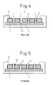
- Fig. 4 is a view showing a state in which, while the silicon substrate 1, the adhesive film 4 and the metallic foil 5 are fixed to each other by the jig 6, etching is conducted toward the through-holes 2 from an upper surface of the silicon substrate 1 so that drilling can be conducted to the adhesive film 4 at portions corresponding to the through-holes 2.
- etching is conducted by means of plasma etching by which plasma is irradiated into the through-holes 2.
- Fig. 5 is a view showing a step in which the jig 6 is dipped in a plating solution and electrolytic plating is conducted while the piece of metallic foil 5 is used as a cathode as mentioned above and the metal 11 is precipitated in the through-holes so that these through-holes are plugged with the metal.
- the plating metal 11 is copper, the conductivity of which is high.
- the piece of metallic foil or the metallic sheet 5 is made to adhere to the reverse surface of the silicon substrate 1 so that the piece of metallic foil or the metallic sheet 5 can be used as a cathode and further when the cathode is exposed in portions corresponding to the through-holes 2 on the silicon substrate 1, it is possible to precipitate the metal 11 only in the portions corresponding to the through-holes 2.
- Fig. 6 is a view showing a step in which the piece of metallic foil 5, which has been made to adhere to the reverse side of the silicon substrate 1, is peeled off and both surfaces of the silicon substrate including the metal 11 plugged in the through-holes 2 are smoothed. Due to the foregoing, the silicon substrate becomes to have a shape 9 like a strip. In this step of smoothing both faces of the silicon substrate 1, it is preferable to adopt chemical mechanical polishing (CMP).
- CMP chemical mechanical polishing
- Fig. 7 is a view showing a step in which high pressure annealing is conducted on the silicon substrate 1.
- heat treatment is conducted in an atmosphere of high-pressure argon gas.
- the heating temperature is set at about 350°C and the pressure is set at about 150 Mpa.
- the heating temperature must be a value sufficiently lower than the melting points of copper and aluminum so that, of course, the plugged metal (for example, copper) and the aluminum wiring (not shown) on the silicon substrate 1 cannot be melted.
- the processing time must be a period of time in which the plugged copper can be made precise and dense.
- the plugs can be composed of precise and dense metal.
- a minute gap 20 caused by minute voids exist between the plated metal 1 and the oxidized insulating film 3 on the inner wall of the through-hole 2, however, after the completion of high pressure annealing, this gap is filled with metal 22 as shown in Fig. 7. Due to the foregoing, the reliability of the via wiring can be enhanced, and deterioration of the yield can be effectively prevented.
- the plugs can be composed of precise and dense metal.
- the reliability of the via wiring can be enhanced, and deterioration of the yield can be effectively prevented. Therefore, on the silicon substrate used for chip level three-dimensional mounting, the through-holes can be plugged with copper by means of plating.
- the chip level three-dimensional mounting is realized, it becomes possible to manufacture a high-performance semiconductor chip. Further, operation can be performed at high speed, and furthermore, compact mounting can be performed.
Landscapes
- Engineering & Computer Science (AREA)
- Manufacturing & Machinery (AREA)
- Microelectronics & Electronic Packaging (AREA)
- Internal Circuitry In Semiconductor Integrated Circuit Devices (AREA)
- Printing Elements For Providing Electric Connections Between Printed Circuits (AREA)
Abstract
Description
Claims (7)
- A method of plugging through-holes in a silicon substrate comprising the following steps of:providing the silicon substrate having first and second surfaces with through-holes penetrating from the first surface to the second surface;forming an insulating film on the first and second surfaces of the silicon substrate including inner wall faces of the through-holes;adhering a conductor plane to the second surface of the silicon substrate by means of an adhesive;etching the adhesive via the through-holes from the first surface of the silicon substrate to drill the adhesive so that the conductor plane is exposed in inside of the through-holes;filling the through-holes with a metal by plating the metal using the conductor plane as an electrode from the first surface of the silicon substrate;peeling off the conductor plane and smoothing the first and second surfaces of the silicon substrate including the filled metal; andconducting a high-pressure annealing on the silicon substrate.
- A plugging method as set forth in claim 1, wherein the insulating film formed on the first and second surfaces of the silicon substrate including the inner wall faces of the through-holes is an oxide film formed by means of chemical vapor-deposition or thermal treatment.
- A plugging method as set forth in claim 1, wherein the etching step of the adhesive film is conducted by a plasma etching.
- A plugging method as set forth in claim 1, wherein smoothing step of the first and second surfaces of the silicon substrate is conducted by chemical mechanical polishing.
- A plugging method as set forth in claim 1, wherein the step of high-pressure annealing on the silicon substrate is conducted under a pressure of 150 Mpa at a temperature of 350°C in an argon atmosphere.
- A plugging method as set forth in claim 1, wherein the adhesive is an adhesive film.
- A plugging method as set forth in claim 1, wherein the metallic plane is a copper foil.
Applications Claiming Priority (2)
| Application Number | Priority Date | Filing Date | Title |
|---|---|---|---|
| JP2002178902 | 2002-06-19 | ||
| JP2002178902A JP3904484B2 (en) | 2002-06-19 | 2002-06-19 | Through-hole plugging method of silicon substrate |
Publications (3)
| Publication Number | Publication Date |
|---|---|
| EP1376686A2 true EP1376686A2 (en) | 2004-01-02 |
| EP1376686A3 EP1376686A3 (en) | 2004-04-21 |
| EP1376686B1 EP1376686B1 (en) | 2005-08-31 |
Family
ID=29717499
Family Applications (1)
| Application Number | Title | Priority Date | Filing Date |
|---|---|---|---|
| EP03291402A Expired - Lifetime EP1376686B1 (en) | 2002-06-19 | 2003-06-12 | Method of plugging through-holes in silicon substrate |
Country Status (6)
| Country | Link |
|---|---|
| US (1) | US6815348B2 (en) |
| EP (1) | EP1376686B1 (en) |
| JP (1) | JP3904484B2 (en) |
| KR (1) | KR100999907B1 (en) |
| CN (1) | CN1310309C (en) |
| TW (1) | TWI294160B (en) |
Cited By (1)
| Publication number | Priority date | Publication date | Assignee | Title |
|---|---|---|---|---|
| EP1612859A2 (en) | 2004-06-29 | 2006-01-04 | Shinko Electric Industries Co., Ltd. | Through electrode and method for forming the same |
Families Citing this family (42)
| Publication number | Priority date | Publication date | Assignee | Title |
|---|---|---|---|---|
| JP3836375B2 (en) * | 2002-01-11 | 2006-10-25 | シャープ株式会社 | Manufacturing method of semiconductor device |
| CN100449799C (en) * | 2004-09-29 | 2009-01-07 | 晶元光电股份有限公司 | Method for forming packaging substrate of light-emitting diode |
| JP4698296B2 (en) | 2005-06-17 | 2011-06-08 | 新光電気工業株式会社 | Manufacturing method of semiconductor device having through electrode |
| JP2006351935A (en) * | 2005-06-17 | 2006-12-28 | Shinko Electric Ind Co Ltd | Semiconductor chip mounting substrate and semiconductor device using the same |
| JP4650117B2 (en) * | 2005-06-21 | 2011-03-16 | パナソニック電工株式会社 | Manufacturing method of semiconductor device |
| JP4552770B2 (en) * | 2005-06-21 | 2010-09-29 | パナソニック電工株式会社 | Method for forming through wiring on semiconductor substrate |
| JP4889974B2 (en) * | 2005-08-01 | 2012-03-07 | 新光電気工業株式会社 | Electronic component mounting structure and manufacturing method thereof |
| JP4581915B2 (en) * | 2005-08-26 | 2010-11-17 | パナソニック電工株式会社 | Manufacturing method of through-hole wiring |
| JP4758712B2 (en) * | 2005-08-29 | 2011-08-31 | 新光電気工業株式会社 | Manufacturing method of semiconductor device |
| JP4828182B2 (en) * | 2005-08-31 | 2011-11-30 | 新光電気工業株式会社 | Manufacturing method of semiconductor device |
| JP4755545B2 (en) * | 2006-07-11 | 2011-08-24 | 新光電気工業株式会社 | Substrate manufacturing method |
| JP4807272B2 (en) * | 2007-02-05 | 2011-11-02 | パナソニック電工株式会社 | Method for forming through-hole wiring on semiconductor wafer |
| JP5137059B2 (en) | 2007-06-20 | 2013-02-06 | 新光電気工業株式会社 | Electronic component package, manufacturing method thereof, and electronic component device |
| JP5367616B2 (en) * | 2009-02-23 | 2013-12-11 | 新光電気工業株式会社 | Wiring board and manufacturing method thereof |
| JP5563785B2 (en) * | 2009-05-14 | 2014-07-30 | 新光電気工業株式会社 | Semiconductor package and manufacturing method thereof |
| TWI392069B (en) * | 2009-11-24 | 2013-04-01 | 日月光半導體製造股份有限公司 | Package structure and packaging process |
| TWI446420B (en) | 2010-08-27 | 2014-07-21 | 日月光半導體製造股份有限公司 | Carrier separation method for semiconductor process |
| TWI445152B (en) | 2010-08-30 | 2014-07-11 | 日月光半導體製造股份有限公司 | Semiconductor structure and manufacturing method thereof |
| US9007273B2 (en) | 2010-09-09 | 2015-04-14 | Advances Semiconductor Engineering, Inc. | Semiconductor package integrated with conformal shield and antenna |
| TWI434387B (en) | 2010-10-11 | 2014-04-11 | 日月光半導體製造股份有限公司 | Semiconductor device having via hole and package structure of semiconductor device having via hole and manufacturing method thereof |
| TWI527174B (en) | 2010-11-19 | 2016-03-21 | 日月光半導體製造股份有限公司 | Package structure with semiconductor components |
| TWI445155B (en) | 2011-01-06 | 2014-07-11 | 日月光半導體製造股份有限公司 | Stacked package structure and manufacturing method thereof |
| US8853819B2 (en) | 2011-01-07 | 2014-10-07 | Advanced Semiconductor Engineering, Inc. | Semiconductor structure with passive element network and manufacturing method thereof |
| US8541883B2 (en) | 2011-11-29 | 2013-09-24 | Advanced Semiconductor Engineering, Inc. | Semiconductor device having shielded conductive vias |
| US8629061B2 (en) * | 2012-02-08 | 2014-01-14 | Gtat Corporation | Method for three-dimensional packaging of electronic devices |
| US8975157B2 (en) | 2012-02-08 | 2015-03-10 | Advanced Semiconductor Engineering, Inc. | Carrier bonding and detaching processes for a semiconductor wafer |
| US8963316B2 (en) | 2012-02-15 | 2015-02-24 | Advanced Semiconductor Engineering, Inc. | Semiconductor device and method for manufacturing the same |
| US8786060B2 (en) | 2012-05-04 | 2014-07-22 | Advanced Semiconductor Engineering, Inc. | Semiconductor package integrated with conformal shield and antenna |
| US9153542B2 (en) | 2012-08-01 | 2015-10-06 | Advanced Semiconductor Engineering, Inc. | Semiconductor package having an antenna and manufacturing method thereof |
| US8937387B2 (en) | 2012-11-07 | 2015-01-20 | Advanced Semiconductor Engineering, Inc. | Semiconductor device with conductive vias |
| US8952542B2 (en) | 2012-11-14 | 2015-02-10 | Advanced Semiconductor Engineering, Inc. | Method for dicing a semiconductor wafer having through silicon vias and resultant structures |
| US9406552B2 (en) | 2012-12-20 | 2016-08-02 | Advanced Semiconductor Engineering, Inc. | Semiconductor device having conductive via and manufacturing process |
| US8841751B2 (en) | 2013-01-23 | 2014-09-23 | Advanced Semiconductor Engineering, Inc. | Through silicon vias for semiconductor devices and manufacturing method thereof |
| US9978688B2 (en) | 2013-02-28 | 2018-05-22 | Advanced Semiconductor Engineering, Inc. | Semiconductor package having a waveguide antenna and manufacturing method thereof |
| US9089268B2 (en) | 2013-03-13 | 2015-07-28 | Advanced Semiconductor Engineering, Inc. | Neural sensing device and method for making the same |
| US9173583B2 (en) | 2013-03-15 | 2015-11-03 | Advanced Semiconductor Engineering, Inc. | Neural sensing device and method for making the same |
| US8987734B2 (en) | 2013-03-15 | 2015-03-24 | Advanced Semiconductor Engineering, Inc. | Semiconductor wafer, semiconductor process and semiconductor package |
| JP7208011B2 (en) * | 2016-11-28 | 2023-01-18 | 三井金属鉱業株式会社 | Multilayer wiring board manufacturing method |
| CN109770438B (en) * | 2019-03-25 | 2023-07-25 | 云南中烟工业有限责任公司 | Film-coated silicon-based electronic cigarette atomization chip and preparation method thereof |
| CN110634792B (en) * | 2019-09-26 | 2023-01-24 | 上海航天电子通讯设备研究所 | A method of manufacturing an electrical interconnect substrate |
| TW202518607A (en) * | 2023-10-30 | 2025-05-01 | 強茂股份有限公司 | Manufacturing method of pre-molded packaging lead frame |
| US20250203776A1 (en) * | 2023-12-14 | 2025-06-19 | Unimicron Technology Corp. | Substrate structure and manufacturing method thereof |
Family Cites Families (9)
| Publication number | Priority date | Publication date | Assignee | Title |
|---|---|---|---|---|
| US4348253A (en) * | 1981-11-12 | 1982-09-07 | Rca Corporation | Method for fabricating via holes in a semiconductor wafer |
| JPS6132363A (en) * | 1984-07-23 | 1986-02-15 | Hitachi Ltd | Fuel cell power generation system |
| JPH01258457A (en) * | 1988-04-08 | 1989-10-16 | Nec Corp | Semiconductor integrated circuit package structure and manufacture thereof |
| JP2773366B2 (en) * | 1990-03-19 | 1998-07-09 | 富士通株式会社 | Method of forming multilayer wiring board |
| JPH11288973A (en) | 1998-04-01 | 1999-10-19 | Canon Inc | Semiconductor connection structure, semiconductor connection method, and semiconductor device |
| US6114098A (en) * | 1998-09-17 | 2000-09-05 | International Business Machines Corporation | Method of filling an aperture in a substrate |
| JP2000353703A (en) | 1999-06-11 | 2000-12-19 | Sony Corp | Method for manufacturing semiconductor device |
| JP2001060621A (en) * | 1999-08-20 | 2001-03-06 | Kobe Steel Ltd | Manufacture of semiconductor device |
| US6399486B1 (en) * | 1999-11-22 | 2002-06-04 | Taiwan Semiconductor Manufacturing Company | Method of improved copper gap fill |
-
2002
- 2002-06-19 JP JP2002178902A patent/JP3904484B2/en not_active Expired - Fee Related
-
2003
- 2003-06-12 EP EP03291402A patent/EP1376686B1/en not_active Expired - Lifetime
- 2003-06-12 US US10/459,609 patent/US6815348B2/en not_active Expired - Lifetime
- 2003-06-18 TW TW092116567A patent/TWI294160B/en not_active IP Right Cessation
- 2003-06-18 CN CNB031376754A patent/CN1310309C/en not_active Expired - Fee Related
- 2003-06-18 KR KR1020030039466A patent/KR100999907B1/en not_active Expired - Fee Related
Cited By (4)
| Publication number | Priority date | Publication date | Assignee | Title |
|---|---|---|---|---|
| EP1612859A2 (en) | 2004-06-29 | 2006-01-04 | Shinko Electric Industries Co., Ltd. | Through electrode and method for forming the same |
| EP1612859A3 (en) * | 2004-06-29 | 2006-02-01 | Shinko Electric Industries Co., Ltd. | Through electrode and method for forming the same |
| CN100461357C (en) * | 2004-06-29 | 2009-02-11 | 新光电气工业株式会社 | Penetrating electrode and method for forming same |
| US7498259B2 (en) | 2004-06-29 | 2009-03-03 | Shinko Electric Industries Co., Ltd. | Through electrode and method for forming the same |
Also Published As
| Publication number | Publication date |
|---|---|
| EP1376686A3 (en) | 2004-04-21 |
| KR20030097673A (en) | 2003-12-31 |
| TWI294160B (en) | 2008-03-01 |
| TW200402836A (en) | 2004-02-16 |
| JP3904484B2 (en) | 2007-04-11 |
| US6815348B2 (en) | 2004-11-09 |
| KR100999907B1 (en) | 2010-12-13 |
| CN1310309C (en) | 2007-04-11 |
| JP2004022990A (en) | 2004-01-22 |
| EP1376686B1 (en) | 2005-08-31 |
| CN1467819A (en) | 2004-01-14 |
| US20030235982A1 (en) | 2003-12-25 |
Similar Documents
| Publication | Publication Date | Title |
|---|---|---|
| EP1376686B1 (en) | Method of plugging through-holes in silicon substrate | |
| US4808273A (en) | Method of forming completely metallized via holes in semiconductors | |
| EP0260857B1 (en) | Multilayer wiring substrate | |
| TW591765B (en) | Method of making electronic element-mounted substrate | |
| EP1489658B1 (en) | Method for manufacturing semiconductor package | |
| JP6840935B2 (en) | Wiring circuit board manufacturing method | |
| CN107567651B (en) | Wiring board with through-electrode and method of manufacturing the same | |
| CN209526941U (en) | A circuit board with heat dissipation structure | |
| EP2056343A2 (en) | Silicon interposer producing method, silicon interposer and seminconductor device package and semiconductor device incorporating silicon interposer | |
| KR20040097899A (en) | Method of production of semiconductor device | |
| JPH05304223A (en) | Manufacture of electronic component mounting board | |
| JPS63114198A (en) | Multilayer printed circuit board structure | |
| JP2004119606A (en) | Semiconductor substrate through hole filling method and semiconductor substrate | |
| JP2003273510A (en) | Printed circuit board manufacturing method | |
| JPH11298141A (en) | Electronic device manufacturing method | |
| CN114980575A (en) | Half-side metallized half-side non-metallized blind groove processing method and printed circuit board | |
| JP5028126B2 (en) | Dielectric substrate manufacturing method | |
| CN117098324B (en) | Method for preparing ceramic circuit board | |
| JP2004087862A (en) | Tape carrier for semiconductor device | |
| US7371682B2 (en) | Production method for electronic component and electronic component | |
| KR100593211B1 (en) | Wafer-Through Electrode Manufacturing Method | |
| CN113766758B (en) | Three-dimensional circuit generation method and circuit board | |
| JP2003318507A (en) | Method of manufacturing circuit board | |
| KR101133120B1 (en) | Maunfacturing method for semiconductor package board | |
| CN118973106A (en) | A method for manufacturing a buried circuit carrier with reduced or no circuit subsidence |
Legal Events
| Date | Code | Title | Description |
|---|---|---|---|
| PUAI | Public reference made under article 153(3) epc to a published international application that has entered the european phase |
Free format text: ORIGINAL CODE: 0009012 |
|
| AK | Designated contracting states |
Kind code of ref document: A2 Designated state(s): AT BE BG CH CY CZ DE DK EE ES FI FR GB GR HU IE IT LI LU MC NL PT RO SE SI SK TR |
|
| AX | Request for extension of the european patent |
Extension state: AL LT LV MK |
|
| PUAL | Search report despatched |
Free format text: ORIGINAL CODE: 0009013 |
|
| RAP1 | Party data changed (applicant data changed or rights of an application transferred) |
Owner name: SHINKO ELECTRIC INDUSTRIES CO., LTD. |
|
| AK | Designated contracting states |
Kind code of ref document: A3 Designated state(s): AT BE BG CH CY CZ DE DK EE ES FI FR GB GR HU IE IT LI LU MC NL PT RO SE SI SK TR |
|
| AX | Request for extension of the european patent |
Extension state: AL LT LV MK |
|
| RIC1 | Information provided on ipc code assigned before grant |
Ipc: 7H 01L 21/768 A Ipc: 7H 05K 3/42 B |
|
| 17P | Request for examination filed |
Effective date: 20040514 |
|
| AKX | Designation fees paid |
Designated state(s): FR |
|
| GRAP | Despatch of communication of intention to grant a patent |
Free format text: ORIGINAL CODE: EPIDOSNIGR1 |
|
| REG | Reference to a national code |
Ref country code: DE Ref legal event code: 8566 |
|
| GRAS | Grant fee paid |
Free format text: ORIGINAL CODE: EPIDOSNIGR3 |
|
| GRAA | (expected) grant |
Free format text: ORIGINAL CODE: 0009210 |
|
| AK | Designated contracting states |
Kind code of ref document: B1 Designated state(s): FR |
|
| ET | Fr: translation filed | ||
| PLBE | No opposition filed within time limit |
Free format text: ORIGINAL CODE: 0009261 |
|
| STAA | Information on the status of an ep patent application or granted ep patent |
Free format text: STATUS: NO OPPOSITION FILED WITHIN TIME LIMIT |
|
| 26N | No opposition filed |
Effective date: 20060601 |
|
| REG | Reference to a national code |
Ref country code: FR Ref legal event code: PLFP Year of fee payment: 13 |
|
| PGFP | Annual fee paid to national office [announced via postgrant information from national office to epo] |
Ref country code: FR Payment date: 20150608 Year of fee payment: 13 |
|
| REG | Reference to a national code |
Ref country code: FR Ref legal event code: ST Effective date: 20170228 |
|
| PG25 | Lapsed in a contracting state [announced via postgrant information from national office to epo] |
Ref country code: FR Free format text: LAPSE BECAUSE OF NON-PAYMENT OF DUE FEES Effective date: 20160630 |