EP1376669A1 - Plasma processing device - Google Patents
Plasma processing device Download PDFInfo
- Publication number
- EP1376669A1 EP1376669A1 EP02708711A EP02708711A EP1376669A1 EP 1376669 A1 EP1376669 A1 EP 1376669A1 EP 02708711 A EP02708711 A EP 02708711A EP 02708711 A EP02708711 A EP 02708711A EP 1376669 A1 EP1376669 A1 EP 1376669A1
- Authority
- EP
- European Patent Office
- Prior art keywords
- microwave
- processing apparatus
- plasma
- plasma processing
- dielectric member
- Prior art date
- Legal status (The legal status is an assumption and is not a legal conclusion. Google has not performed a legal analysis and makes no representation as to the accuracy of the status listed.)
- Granted
Links
Images





Classifications
-
- H—ELECTRICITY
- H01—ELECTRIC ELEMENTS
- H01J—ELECTRIC DISCHARGE TUBES OR DISCHARGE LAMPS
- H01J37/00—Discharge tubes with provision for introducing objects or material to be exposed to the discharge, e.g. for the purpose of examination or processing thereof
- H01J37/32—Gas-filled discharge tubes
- H01J37/32009—Arrangements for generation of plasma specially adapted for examination or treatment of objects, e.g. plasma sources
- H01J37/32192—Microwave generated discharge
- H01J37/32211—Means for coupling power to the plasma
- H01J37/3222—Antennas
-
- H—ELECTRICITY
- H10—SEMICONDUCTOR DEVICES; ELECTRIC SOLID-STATE DEVICES NOT OTHERWISE PROVIDED FOR
- H10P—GENERIC PROCESSES OR APPARATUS FOR THE MANUFACTURE OR TREATMENT OF DEVICES COVERED BY CLASS H10
- H10P95/00—Generic processes or apparatus for manufacture or treatments not covered by the other groups of this subclass
-
- H—ELECTRICITY
- H01—ELECTRIC ELEMENTS
- H01J—ELECTRIC DISCHARGE TUBES OR DISCHARGE LAMPS
- H01J37/00—Discharge tubes with provision for introducing objects or material to be exposed to the discharge, e.g. for the purpose of examination or processing thereof
- H01J37/32—Gas-filled discharge tubes
- H01J37/32009—Arrangements for generation of plasma specially adapted for examination or treatment of objects, e.g. plasma sources
- H01J37/32192—Microwave generated discharge
-
- H—ELECTRICITY
- H01—ELECTRIC ELEMENTS
- H01J—ELECTRIC DISCHARGE TUBES OR DISCHARGE LAMPS
- H01J37/00—Discharge tubes with provision for introducing objects or material to be exposed to the discharge, e.g. for the purpose of examination or processing thereof
- H01J37/32—Gas-filled discharge tubes
- H01J37/32009—Arrangements for generation of plasma specially adapted for examination or treatment of objects, e.g. plasma sources
- H01J37/32192—Microwave generated discharge
- H01J37/32211—Means for coupling power to the plasma
- H01J37/32229—Waveguides
-
- H—ELECTRICITY
- H01—ELECTRIC ELEMENTS
- H01J—ELECTRIC DISCHARGE TUBES OR DISCHARGE LAMPS
- H01J37/00—Discharge tubes with provision for introducing objects or material to be exposed to the discharge, e.g. for the purpose of examination or processing thereof
- H01J37/32—Gas-filled discharge tubes
- H01J37/32431—Constructional details of the reactor
- H01J37/3244—Gas supply means
Definitions
- the present invention is generally related to a plasma processing apparatus, and more particularly, to a microwave plasma processing apparatus.
- Plasma processing and plasma processing apparatuses are an indispensable technology for fabricating ultrafine semiconductor devices these days called deep submicron devices or deep subquarter micron devices characterized by a gate length of near 0.1 ⁇ m or less, and for fabricating ultra high-resolution flat-panel display devices including liquid crystal display devices.
- a microwave plasma processing apparatus that uses high-density plasma excited by a microwave electric field, in place of a direct-current magnetic field.
- a plasma processing apparatus that causes excitation of plasma by radiating a microwave into a processing vessel from a planar antenna (radial line slot antenna) having a number of slots disposed so as to form a uniform microwave, such that the microwave electric field causes ionization of a gas in a vacuum vessel.
- the microwave plasma thus formed is characterized by low electron temperature, and damaging or metal contamination of the substrate is avoided. Further, it is possible to form uniform plasma over a large surface area, and it can be easily applied to the fabrication process of a semiconductor device using a large diameter semiconductor substrate and a large size liquid crystal display device.
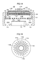
- Figs. 1A and 1B show the construction of a conventional microwave plasma processing apparatus 100 having such a radial line slot antenna, wherein Fig. 1A shows the microwave plasma processing apparatus in a cross-sectional view while Fig. 1B shows the construction of the radial line slot antenna.
- the microwave plasma processing apparatus 100 has a processing chamber 101 evacuated from plural evacuation ports 116, and a stage 115 is formed for holding a substrate 114 to be processed.
- a ring-shaped space 101A is formed around the stage 115, and the plural evacuation ports 116 are formed in communication with the foregoing space 101A at a uniform interval, and hence in axial symmetry with regard to the substrate. Thereby, it becomes possible to evacuate the processing chamber 101 uniformly through the space 101A and the evacuation ports 116.
- a shower plate 103 of plate-like form On the processing chamber 101, there is formed a shower plate 103 of plate-like form at the location corresponding to the substrate 114 on the stage 115 as a part of the outer wall of the processing chamber 101, and the shower plate 103 is sealed with respect to the processing chamber 101 via a seal ring 109, wherein the shower plate 103 is formed of a dielectric material of small loss and includes a large number of apertures 107. Further, a cover plate 102 also of a dielectric material of small loss is provided on the outer side of the shower plate 103, and the cover plate 102 is sealed with respect to the shower plate 103 via another seal ring 108.
- the shower plate 103 is formed with a passage 104 for a plasma gas on the top surface thereof, and each of the plural apertures 107 are formed in communication with the foregoing plasma gas passage 104. Further, there is formed a plasma gas supply passage 108 in the interior of the shower plate 103 in communication with a plasma gas supply port 105 provided on the outer wall of the processing vessel 101.
- the plasma gas of Ar, Kr or the like supplied to the foregoing plasma gas supply port 105 is supplied to the foregoing apertures 107 from the supply passage 108 via the passage 104 and is released into a space 101B underneath the shower plate 103 in the processing vessel 101 from the apertures 107 with substantially uniform concentration.
- a radial line slot antenna 110 having a radiation surface shown in Fig. 1B on the outer side of the cover plate 102 with a separation of 4 - 5 mm from the cover plate 102.
- the radial line slot antenna 110 is connected to an external microwave source (not shown) via a coaxial waveguide 110A and causes excitation of the plasma gas released into the space 101B by the microwave from the microwave source. It should be noted that the gap between the cover plate 102 and the radiation surface of the radial line slot antenna 110 is filled with air.
- the radial line slot antenna 110 is formed of a flat disk-like antenna body 110B connected to an outer waveguide of the coaxial waveguide 110A and a radiation plate 110C is provided on the mouth of the antenna body 110B, wherein the radiation plate 110C is formed with a number of slots 110a and slots 110b wherein slots 110b are formed in a direction crossing the slots 110a perpendicularly as represented in Fig. 1B. Further, a retardation plate 110D of a dielectric film of uniform thickness is inserted between the antenna body 110B and the radiation plate 110C.
- the microwave supplied from the coaxial waveguide 110 spreads between the disk-like antenna body 110B and the radiation plate 110C as it is propagated in the outward radial directions, wherein there occurs a compression of wavelength as a result of the action of the retardation plate 110D.
- the slots 110a and 110b in concentric relationship in correspondence to the wavelength of the radially propagating microwave so as to cross perpendicularly with each other, it becomes possible to emit a plane wave having a circular polarization state in a direction substantially perpendicular to the radiation plate 110C.
- the high-density plasma thus formed is characterized by a low electron temperature and thus no damage is caused to the substrate 114 and no metal contamination occurs due to sputtering of the vessel wall of the processing vessel 101.
- a conductor structure 111 in the processing vessel 101 between the shower plate 103 and the substrate 114 wherein the conductor structure 111 is formed with a number of nozzles 113 supplied with a processing gas from an external processing gas source (not shown) via a processing gas passage 112 formed in the processing vessel 101, and each of the nozzles 113 releases the processing gas supplied thereto into a space 101C between the conductive structure 111 and the substrate 114.
- the conductive structure 111 is formed with openings between adjacent nozzles 113 with a size such that the plasma formed in the space 101B passes efficiently from the space 101B to the space 101C by way of diffusion.
- the processing gas is excited by the high-density plasma formed in the space 101B and uniform plasma processing is conducted on the substrate 114 efficiently and at a high rate, without damaging the substrate or the devices on the substrate, and without contaminating the substrate.
- the microwaves emitted from the radial line slot antenna 110 are blocked by the conductive structure 111 and there is no possibility of such microwaves causing damage to the substrate 114.
- An impedance matching structure is generally provided between a microwave antenna and a waveguide connected to the microwave antenna to inject a weak microwave signal received by the microwave antenna into the waveguide without loss.
- high-power microwaves are provided to the radial line slot antenna 110 through the waveguide, and additionally, reflective microwaves reflected by the plasma formed in the processing vessel 101 are also superimposed on the high-power microwaves in the antenna 110 and the waveguide.
- the impedance matching of the power supply unit connecting the waveguide and the antenna body 110 is much more important than usual.
- Another and more specific object of the present invention is to provide a plasma processing apparatus having a microwave antenna, forming plasma in the processing vessel by providing microwaves from the microwave antenna to the processing vessel through the microwave transparent window, and processing the substrate in the plasma, in which the efficiency of supplying microwaves from the microwave waveguide to the microwave antenna is increased, and the abnormal discharge problem due to the mismatching of impedance at the joint unit between the microwave waveguide and the microwave antenna is eliminated.
- Yet another object of the present invention is to provide a plasma processing apparatus, comprising, a processing vessel defined by an outer. wall and having a stage for holding a substrate to be processed, an evacuation system coupled to said processing vessel, a microwave transparent window provided on said processing vessel as a part of said outer wall, and opposite said substrate held on said stage, a plasma gas supplying part for supplying plasma gas to said processing vessel, a microwave antenna provided on said processing vessel in correspondence to said microwave, and a microwave power source electrically coupled to said microwave antenna, wherein said microwave antenna comprising a coaxial waveguide connected to said microwave power source, said coaxial waveguide having an inner conductor core and an outer conductor tube surrounding said inner conductor core, and an antenna body provided to a point of said coaxial waveguide, said antenna body further comprising a first conductor surface forming a microwave radiation surface coupled with said microwave transparent window, and a second conductor surface opposite said first conductor surface via a dielectric plate, said second conductor surface being connected to said first conductor surface at a peripheral part of said dielectric
- Another object of the present invention is to provide a plasma processing apparatus, comprising, a processing vessel defined by an outer wall and having a stage for holding a substrate to be processed, an evacuation system coupled to said processing vessel, a microwave transparent window provided on said processing vessel as a part of said outer wall, opposite said substrate held on said stage, a plasma gas supplying part for supplying plasma gas to said processing vessel, a microwave antenna provided on said processing vessel in correspondence to said microwave, and a microwave power source electrically coupled to said microwave antenna, wherein said microwave antenna comprising a coaxial waveguide connected to said microwave power source, said coaxial waveguide having an inner conductor core and an outer conductor tube surrounding said inner conductor core, and an antenna body provided to a point of said coaxial waveguide, said antenna body further comprising a first conductor surface forming microwave a radiation surface coupled with said microwave transparent window, and a second conductor surface opposite said first conductor surface via a dielectric plate, said second conductor surface being connected to said first conductor surface'at a peripheral part of said dielectric plate,
- the rapid change in impedance by the joint unit between the microwave waveguide and the microwave antenna is avoided.
- microwaves reflected by the joint unit are efficiently reduced.
- the reflective waves are reduced, abnormal discharge at the joint unit and consequent damage on the antenna caused by the abnormal discharge is avoided.
- the reduction in the reflective waves stabilizes the supply of microwaves to the processing vessel through the microwave transparent window, and makes it possible to form stable plasma in the processing vessel as desired.
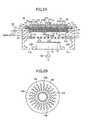
- Figs. 2A and 2B are diagrams showing the construction of a microwave plasma processing apparatus 10 according to a first embodiment of the present invention.
- the microwave plasma processing apparatus 10 includes a processing vessel 11 and a stage 13 provided in the processing vessel 11 for holding a substrate 12 to be processed by an electrostatic chuck, wherein the stage 13 is preferably formed of AlN or Al 2 O 3 by a hot isostatic pressing (HIP) process.
- the processing vessel 11 there are formed two or three evacuation ports 11a in a space 11A surrounding the stage 13 with an equal distance, and hence with an axial symmetry with respect to the substrate 12 on the stage 13.
- the processing vessel 11 is evacuated to a low pressure via the evacuation ports 11a by a gradational lead screw pump.
- the processing vessel 11 is preferably formed of an austenite stainless steel containing Al, and there is formed a protective film of aluminum oxide on the inner wall surface by an oxidizing process. Further, there is formed a disk-shaped shower plate 14 of dense Al 2 O 3 , formed by a HIP process, in the part of the outer wall of the processing vessel 11 corresponding to the substrate 12 as a part of the outer wall, wherein the shower plate 14 includes a large number of nozzle apertures 14A.
- the Al 2 O 3 shower plate 14 thus formed by the HIP process is formed by using an Y 2 O 3 additive and has porosity of 0.03% or less. This means that the Al 2 O 3 shower plate is substantially free from pores or pinholes and has a very large, while not so large as that of AlN, thermal conductivity for a ceramic of 30W/m • K.
- the shower plate 14 is mounted on the processing vessel 11 and sealed thereto via a seal ring 11s, and a cover plate 15 of dense Al 2 O 3 formed also by an HIP process is provided on the shower plate 14 and sealed thereto via a seal ring 11t.
- the shower plate 14 is formed with a depression 14B communicating with each of the nozzle apertures 14A and serving as a plasma gas passage, a side thereof formed by the cover plate 15.
- the depression 14B also communicates with another plasma gas passage 14C formed in the interior of the shower plate 14 in communication with a plasma gas inlet 11p formed on the outer wall of the processing vessel 11.
- the shower plate 14 is held by an extending part 11b formed on the inner wall of the processing vessel 11, wherein the extending part 11b is formed with a round surface at the part holding the shower plate 14 so as to suppress electric discharge.
- plasma gas such as Ar or Kr supplied to the plasma gas inlet 11p is supplied to a space 11B underneath the shower plate 14 uniformly via the apertures 14A after being passed through the passage 14C and the depression 14B in the shower plate 14.
- a radial line slot antenna 20 formed of a disk-shaped slot plate 16 formed with a number of slots 16a and 16b shown in Fig. 3B in intimate contact with the cover plate 15, a disk-shaped antenna body 17 holding the slot plate 16, and a retardation plate 18 of a dielectric material of low loss such as Al 2 O 3 , SiO 2 or Si 3 N 4 sandwiched between the slot plate 16 and the antenna body 17.
- the radial line slot antenna 20 is mounted on the processing vessel 11 and sealed thereto by way of a seal ring 11u, and a microwave of 2.45GHz or 8.3 GHz frequency is fed to the radial line slot antenna 20 from an external microwave source (not shown) via a coaxial waveguide 21.
- the microwave thus supplied is radiated into the interior of the processing vessel from the slots 16a and 16b in the slot plate 16 via the cover plate 15 and the shower plate 14.
- the microwaves cause excitation of plasma in the plasma gas supplied from the apertures 14A in the space 11B underneath the shower plate 14.
- the cover plate 15 and the shower plate 14 are formed of Al 2 O 3 and function as an efficient microwave-transmitting window.
- the plasma gas is held at a pressure of about 6666Pa - 13332Pa (about 50-100Torr) in the foregoing passages 14A - 14C.'
- the microwave plasma processing apparatus 10 of the present embodiment has a ring-shaped groove 11g in a part of the processing vessel 11 so as to be adjacent to the slot plate 16.
- the pressure in the gap formed between the slot plate 16 and the cover plate 15 is reduced and the radial line slot antenna 20 is urged firmly upon the cover plate 15 by the atmospheric pressure.
- a gap includes not only the slots 16a and 16b formed in the slot plate 16 but also a gap formed for various other reasons. It should be noted further that such a gap is sealed by the seal ring 11u provided between the radial line slot antenna 20 and the processing vessel 11.
- an outer waveguide 21A of the coaxial waveguide 21A is connected to the disk-shaped antenna body 17 while a center conductor 21B is connected to the slot plate 16 via an opening formed in the retardation plate 18.
- the microwave fed to the coaxial waveguide 21A is propagated in the outer radial directions between the antenna body 17 and the slot plate 16 and is emitted from the slots 16a and 16b.
- Fig. 2B shows the slots 16a and 16b formed in the slot plate 16.
- the slots 16a are arranged concentrically, and the slots 16b, each corresponding to a slot 16a and being perpendicular to the corresponding slot 16a, are also arranged concentrically.
- the slots 16a and 16b are formed with an interval corresponding to the wavelength of the microwave compressed by the retardation plate 18 in the radial direction of the slot plate 16, and as a result, the microwave is radiated from the slot plate 16 in the form of a near plane wave. Because the slots 16a and the slots 16b are formed in a mutually perpendicular relationship, the microwave thus radiated forms a circularly polarized wave including two perpendicular polarization components.
- a cooling block 19 formed with a cooling water passage 19A on the antenna body 17, and the heat accumulated in the shower plate 14 is absorbed via the radial line slot antenna 20 by cooling the cooling block 19 with cooling water in the cooling water passage 19A.
- the cooling water passage 19A is formed on the cooling block 19 in a spiral form, and cooling water having a controlled oxidation-reduction potential is supplied thereto, wherein the control of the oxidation reduction potential is achieved by eliminating oxygen dissolved in the cooling water by way of bubbling of an H 2 gas.
- desired uniform substrate processing is achieved in a space 11C between the process gas supply structure 31 and the substrate 12.
- Such substrate processing includes plasma oxidation processing, plasma nitridation processing, plasma oxynitridation processing, and plasma CVD processing.
- a reactive ion etching of the substrate 12 by supplying a readily decomposing fluorocarbon gas such as C 4 F 8 , C 5 F 8 or C 4 F 6 or an etching gas containing F or Cl from the process gas supply structure 31 to the space 11C and further by applying a high-frequency voltage to the stage 13 from a high-frequency power source 13A.
- a readily decomposing fluorocarbon gas such as C 4 F 8 , C 5 F 8 or C 4 F 6 or an etching gas containing F or Cl from the process gas supply structure 31 to the space 11C and further by applying a high-frequency voltage to the stage 13 from a high-frequency power source 13A.
- the microwave plasma processing apparatus 10 of the present embodiment it is possible to avoid deposition of reaction byproducts on the inner wall of the processing vessel by heating the outer wall of the processing vessel 11 to a temperature of about 150°C. Thereby, the microwave plasma processing apparatus 10 can be operated constantly and with reliability, by merely conducting a dry cleaning process once a day or so.
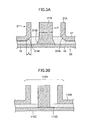
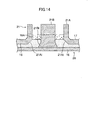
- a taper unit 21Bt of the center conductor 21B is formed at the joint/power supplying unit that connects the coaxial waveguide 21 to the radial line slot antenna 20, so that the radius or the cross sectional area of the center conductor 21B gradually increases towards the slot plate 16.
- Fig. 3A is an expanded diagram showing in detail the construction of the joint/microwave supplying unit between the coaxial waveguide 21 and the radial line slot antenna 20 of the plasma processing apparatus 10 of Fig. 2A.
- the slots 16a and 16b formed on the slot plate 16 are not shown to simplify the drawing.
- the inner conductor 21B has a circular cross section having a diameter of 16.9 mm.
- a 4 mm-thick alumina plate having a relative permittivity of 10.1 is formed between the slot plate 16 and the antenna body 17 as the retardation plate 18.
- the outer waveguide 21A defines a cylindrical space having a circular cross section having an inner diameter of 38.8 mm in which the inner conductor 21B is provided.
- the cross sectional area of the inner conductor 21B is gradually increased from 7 mm above the joint between the inner conductor 21B and the slot plate 16 to the joint.
- the inner conductor 21B has a circular cross section of a diameter of 23 mm at the joint.
- Fig. 4 shows the reflective ratio of microwave provided to the antenna 20 through the waveguide 21 in the case where the radial line slot antenna 20 and the waveguide 21 are used as shown in Fig. 3A, and the parameter "a” shown in Fig. 3A is set at 6.4 mm.
- the reflective ratio is indicated by "•”.
- "*" shown in Fig. 4 indicates a reflective ratio of the construction shown in Fig. 3B to which the taper units 21At and 21Bt are not provided.
- the reflective microwave includes not only the microwave reflected by the joint/supplying unit between the waveguide 21 the radial line antenna 20, but also the microwave reflected by the plasma.
- the reflective ratio is about -2 dB regardless of a frequency, which means about 80% of the microwave is reflectively returned to the waveguide 21 and the microwave source connected to the waveguide 21.
- the reflective ratio depends on the frequency of the microwave.
- the reflective ratio becomes the minimum -23 dB (about 14%) in the neighborhood of 2.4 GHz at which the plasma is excited.
- Fig. 5 shows a microwave reflection factor measured by a power monitor provided between the waveguide 21 and the microwave source in the case of the antenna construction shown in Fig. 3A under the following condition: the inner pressure in the processing vessel being set at 133 Pa (about 1 Torr), Ar and O 2 being supplied from the shower plate 14 at a flux of 690 SCCM and 23 SCCM, respectively, and microwaves of a frequency 2.45 GHz and a power of 1.6 kW is supplied from the waveguide 21 to the radial line slot antenna 20.
- the reflective factor includes not only the reflection of microwave by the joint between the waveguide 21 and the antenna 20, but also the reflection by the plasma formed under the shower plate 14 in the processing vessel 11.
- the reflective ratio is about 80% (the factor of reflection ⁇ 0.8), but in the case of the joint construction of Fig. 3A, the reflective ratio is reduced to about 30% (the factor of reflection ⁇ 0.3) and substantially constant. Since the reflection ratio at the joint unit between the coaxial waveguide 21 and the radial line antenna 20 is about 14% as shown in Fig. 4, the reflective ratio of about 30% as shown in Fig. 5 includes the reflection by the plasma.
- Fig. 6 is a bottom view showing the construction of the process gas supply structure 31 of Fig. 2A.
- the process gas supply structure 31 is formed by a conductive body such as an Al alloy containing Mg or a stainless steel added with Al.
- the lattice shaped gas passage 31A is connected to the process gas inlet port 11r at a process gas supply port 31R and releases the process gas uniformly into the foregoing space 11C from the process gas nozzle apertures 31B formed at the bottom surface. Further, openings 31C are formed in the process gas supply structure 31 between the adjacent process gas passages 31A for passing the plasma or the process gas contained in the plasma therethrough.
- the process gas supply structure 31 is formed of an Al alloy containing Mg, it is preferable to form a fluoride film on the surface thereof.
- the process gas supplying structure 31 is formed of a stainless steel added with Al, it is preferable to form a passivation film of aluminum oxide on the surface thereof.
- the energy of incident plasma is low because of the low electron temperature of the excited plasma, and the problem of metal contamination of the substrate 12 by the sputtering of the process gas supply structure 31 is avoided.
- the lattice shaped process gas passages 31A and the process gas nozzle apertures 31B are formed so as to encompass an area slightly larger than the substrate 12 represented in Fig. 4.by a broken line.
- the process gas supply structure 31 can form a shunting plane of the microwaves by setting the interval between the lattice shaped process gas passages 31A shorter than the microwave wavelength.
- the microwave excitation of plasma takes place only in the space 11B, and there occurs excitation of the process gas in the space 11C including the surface of the substrate 12 by the plasma that has caused diffusion from the excitation space 11B.
- such a construction can prevent the substrate from being exposed directly to the microwave at the time of ignition of the plasma, and thus, damaging of the substrate by the microwave is avoided.
- the supply of the process gas is controlled uniformly by the process gas supply structure 31, and the problem of excessive dissociation of the process gas on the surface of the substrate 12 is eliminated.
- the microwave plasma processing apparatus 10 is effective for fabricating various semiconductor devices of different generations characterized by different design rules.
- Fig. 7 shows the schematic construction of the microwave source connected to the coaxial waveguide 21 of Fig. 2A.
- the coaxial waveguide is connected to an edge of the waveguide extending from an oscillation part 25 including therein a magnetron 25A oscillating at the frequency of 2.45GHz or 8.3GHz via an isolator 24, a power monitor 23 and a tuner 22 in this order.
- the microwave formed by the oscillator 25 is supplied to the radial line slot antenna 20, and the microwave reflected back from the high-density plasma formed in the plasma processing apparatus 10 is returned again to the radial line slot antenna 20 after conducting an impedance adjustment by the tuner 22.
- the isolator 24 is an element having directivity and functions so as to protect the magnetron 25A in the oscillation part 25 from the reflection wave.
- the rapid change in impedance caused by the joint is reduced by forming the taper units 21At and 21Bt at the joint, or the power supplying unit, between the coaxial waveguide 21 and the radial line slot antenna 20.
- the reflection of microwaves caused by the rapid change in impedance is suppressed, which makes the supplying of microwaves from the coaxial waveguide 21 to the antenna 20 stable.
- the microwave plasma processing apparatus 10 as shown in a variation shown in Fig. 8, it is possible to replace the taper faces 21At and 21Bt with round faces 21Ar and 21Br, respectively.
- the change in impedance caused by the joint is further reduced by forming the round faces, which results in further efficient suppressing of the reflective wave.
- the distance between the shower plate 14 exposed to the heat caused by the plasma and the cooling unit is reduced substantially, compared with the conventional microwave plasma processing apparatus of Figs. 1A and 1B.
- a material such as Al 2 O 3 having a small dielectric loss and also a small thermal conductivity for the microwave transmission window in place of AlN, which is characterized by large dielectric loss.
- the gas including the reaction byproduct formed in the space 11C as a result of the substrate processing forms a stable gas flow to the space 11A at the outer surrounding area because of the reduced distance between the shower plate 14 and the substrate 12 facing the shower plate 14, and the byproduct is removed from the space 11C quickly.
- Fig. 9 shows the construction of the joint/supplying unit between the coaxial waveguide 21 and the radial line antenna 20 according to a second embodiment of the present invention.
- portions previously described are referred to by the same reference numerals, and their description will be omitted.
- the outer waveguide 21A constructing the coaxial waveguide 21 and the. body 17 of the radial line antenna 20 are connected perpendicularly to each other forming the joint/supplying unit that is perpendicularly bent.
- the inner conductor 21B is also connected to the slot plate 16 perpendicularly.
- the retardation plate 18 is made of Al 2 O 3 having a high relative permittivity, and a ring-shaped member 18A made of SiO 2 , for example, is formed between the outer waveguide 21A and the inner conductor 21B so that an end of the member 18A contacts the retardation plate 18.
- the length of the member 18A can be optimized based on the property of the antenna structure of the coaxial waveguide 21 and the antenna 20.
- the second edge face opposing the first edge face in contact with the retardation plate 18 is exposed to air.
- the ring-shaped member 18A may be made of sintered mixture of SiO 2 and Si 3 N 4 having different permittivity, and the mixture ratio of SiO 2 and Si 3 N 4 in the ring-shaped member 18A may be controlled so that the permittivity continuously increases from the first edge face to the second edge face.
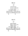
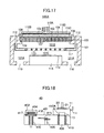
- Fig. 12 shows the construction of the joint unit between the coaxial waveguide 21 and the radial line antenna 20 according to another variation of the present embodiment.
- Fig. 12 portions previously described are referred to by the same reference numeral, and their description will be omitted.
- the second edge face of the ring-shaped member 18A is considered to be a taper surface, and the thickness of the ring-shaped member 18A is linearly increased toward the retardation plate 18.
- the impedance of the joint/supplying unit increases continuously toward the retardation plate 18, and reflection caused by the rapid change in impedance is reduced, which results in an efficient and stable supply of microwaves.
- the ring-shaped member 18A may be coupled with the construction of Fig. 3A having taper surfaces 21At and 21Bt.
- the ring-shaped member 18A is not limited to that of Fig. 9, but may be any construction of Figs. 9 through 13.
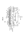
- Fig. 15 is a diagram showing the construction of a plasma processing apparatus 10A according to a third embodiment of the present invention.
- the parts described earlier are referred to by the same reference numerals, and their description is omitted.
- the shower plate 14 is removed, and a plurality of plasma gas inlets 11P are formed, preferably in symmetry, in communication with the gas passage 11p in the processing vessel 11.
- the construction is simplified, and the fabrication cost can be reduced substantially.
- the reflection of microwaves is reduced by forming the taper surfaces 21At and 21Bt in the joint/supplying unit between the radial line slot antenna 20 and the coaxial waveguide 21, which results in an increase in the power supplying efficiency, a reduction in abnormal discharge caused by the reflective waves, and an increased stability of the plasma formation.
- the construction of the joint unit is not limited to that shown in Fig. 3A, and any construction of Figs. 8 through 14 can be used.
- Fig. 16 is a diagram showing the construction of a microwave plasma processing apparatus 10B according to a fourth embodiment of the present invention.
- parts that have been previously described are referred to by the same numerals, and their description will be omitted.
- the process gas supply structure 31 is removed. Additionally, the entire face of the extending part 11b holding the shower plate 14 is rounded out.
- the plasma processing apparatus 10B thus constructed cannot perform film-forming or etching by supplying a process gas besides the plasma gas since the lower shower plate 31 is removed.
- the plasma processing apparatus 10B can form an oxidized layer, a nitrified layer, or an oxidized-nitrified layer by supplying an oxidizing gas or a nitrifying gas from the shower plate 14 together with the plasma gas.
- the reflection of microwaves is reduced by forming the taper surfaces 21At and 21Bt in the joint/supplying unit between the radial line slot antenna 20 and the coaxial waveguide 21, which results in an increase in the power supplying efficiency, a reduction in abnormal discharge caused by the reflective waves, and an increased stability of the plasma formation.
- the construction of the joint unit is not limited to that shown in Fig. 3A, and any construction of Figs. 8 through 14 can be used.
- the joint/supplying structure according to the present invention is not limited to the plasma processing apparatus 10 of Fig. 2A or its variation, and is applicable to the plasma processing apparatus 100 using a conventional radial line slot antenna previously described by referring to Figs. 1A and 1B.
- Fig. 17 shows the construction of a plasma processing apparatus 100A according to a fifth embodiment of the present invention using the joint/supplying structure of the present invention.
- the parts previously described are referred to by the same numerals, and their description will be omitted.
- the plasma processing apparatus 100A has substantially the same construction as the conventional plasma processing apparatus 100, but is different in that the plasma processing apparatus 100A includes taper surfaces similar to the taper surfaces 21At and 21Bt in the joint unit between the coaxial waveguide 110A and the radial slot antenna body 110B or the slot plate 110D.
- the reflection of microwaves is reduced by forming the taper surfaces in the joint/supplying unit between the coaxial waveguide 110A and the radial line slot antenna, which results in an increase in the power supplying efficiency, a reduction in abnormal discharge caused by the reflective waves, and an increased stability of the plasma formation.
- the construction of the joint unit is not limited to that shown in Fig. 3A, and any construction of Figs. 8 through 14 can be used.
- Fig. 18 is a cross sectional view showing the entire construction of a semiconductor fabrication apparatus 40 according to a sixth embodiment of the present invention including the microwave plasma processing apparatus 10 of Figs. 2A and 2B.
- the semiconductor fabrication apparatus 40 includes a vacuum transfer room 401 provided with a robot 405 having a transportation arm 415, and the microwave plasma processing apparatus 10 is formed on the top face of the vacuum transfer room 401.
- the stage 13 can be moved up and down by a cylinder 406 covered by a bellows 410.
- the substrate 12 is set or taken out by the transportation arm 415.
- the substrate 12 is shut off from the vacuum transfer room 401 by a seal 410A and processed as desired.
- a load lock room 402 having a stage 418 to hold a stack of substrates is provided at another position on the upper side of the vacuum transfer room 401.
- the stage 418 ascends to the end, the' load rock room 402 is shut off from the vacuum transfer room 401 by a seal 417.
- the substrate stack 404 descends to the vacuum transfer room 401, and the transportation arm 415 picks up a substrate from the substrate stack 404 or returns a processed substrate thereto.
- semiconductor fabrication apparatus 40 since a substrate is loaded and unloaded vertically, and not through a side wall, an axially symmetry plasma is formed in the processing vessel 11, and a gas in the processing vessel is exhausted through a plurality of exhaustion ports provided in an axial symmetry by a plurality of pumps. Accordingly, the semiconductor fabrication apparatus 40 can guarantee uniform plasma processing.
- Fig. 19 shows the construction of an exhaustion system of the process unit A.
- each exhaustion port 11a of the processing vessel 11 is connected to a duct D1, and a gas in the processing vessel 11 is exhausted by screw molecular pumps P1 and P2, each having a construction as shown in Figs. 14A and 14B, provided in the duct D1.
- the screw molecular pumps P1 and P2 are connected, at their exhaustion side, to an exhaustion line D2 commonly provided to the other processing units B and C of the semiconductor fabrication apparatus 40.
- the exhaustion line D2 is connected to an exhaustion line D3 commonly provided to the other semiconductor fabrication apparatuses via an intermediate booster pump P3.
- Fig. 20A shows the construction of the screw molecular pumps P1 and P2.
- the screw molecular pump has a cylindrical body 51 and a pump inlet at an end part of the body 51 and a pump outlet on the sidewall of the body 51 near the bottom part.
- a rotor 52 shown in Fig. 20B In the body 51, there is provided a rotor 52 shown in Fig. 20B, and a gradational lead screw 52A is formed on the rotor 52.
- the gradational lead screw 52A has a construction in which there is a large pitch formed at the pump inlet part and the pitch is decreased toward the outlet. Associated with this, the lead angle of the screw is decreased gradually from the inlet side toward the outlet side. Further, the volume of the pump chamber is decreased gradually from the inlet side toward the outlet side.
- the screw molecular pump of Fig. 20A includes a motor 53 provided in the rotor 52, an angle detector 54 detecting the angular position of the rotor 52 and a magnet 55 cooperating with the angle detector 54, wherein the rotor 52 is urged toward the outlet side by an electromagnet mechanism 56.
- Such a screw molecular pump has a simple construction and is operable over a wide pressure range from the atmospheric pressure to several millitorrs with small electric power consumption. Further, the screw pump can obtain a pumping speed reaching 320 mL/min, which is larger than the pumping speed of conventional turbo molecular pumps.
- Fig. 21 shows the construction of a gradational lead screw pump (GLSP) 60 used for the intermediate booster pump P3 for evacuating the screw pumps P1 and P2 in the construction of Fig. 19.
- GLSP gradational lead screw pump
- the gradational lead screw pump includes, in a pump body 61 having an inlet 61A at an end and outlets 63A and 63B at another end, a pair of screw rotors 62A and 62B each changing a screw pitch thereof gradually from an inlet side to an outlet side as shown in Fig. 20B, in a meshing relationship of the screws, wherein the rotors 62A and 62B are driven by a motor 64 via gears 63A and 63B.
- the gradational lead screw pump 60 of such a construction is operable over a wide pressure range from ordinary pressure to a low pressure of as much as 10 -4 Torr, and can achieve a flow rate reaching 2,500 L/min.
- the back pump P4 can operate at the most efficient pressure range by exhausting the exhausted gas from the other semiconductor fabrication apparatus, which results in a substantially reduced power consumption.
- Fig. 22 shows the construction of the gas supplying system cooperating with each of the processing units A - C in the semiconductor fabrication apparatus 40 of Fig. 18.
- the semiconductor fabrication apparatus 40 avoids deposition of reaction byproduct formed associated with the substrate processing on the processing vessel 11 of the microwave plasma processing apparatus 10 by maintaining the processing vessel 11 at a temperature of about 150°C.
- the processing unit of Fig. 19 has a feature that the memory or hysteresis of the preceding processing can be erased completely without conducting a specific cleaning process.
- one or two gases selected fro N 2 , Kr, Ar, H 2 , NF 3 , C 4 F 8 , CHF 3 , O 2 , CO, HBr, SiCl 4 and the like are supplied to the plasma gas inlet port 11p provided on the processing vessel 11 in communication with the shower plate 14 through the first and/or second flow rate control apparatuses FCS1 and FCS2, and one or more gases selected from N 2 , Kr, Ar, H 2 , NF 3 , C 4 F 8 , CHF 3 , O 2 , CO, HBr, SiCl 4 and the like, are supplied to the process gas inlet port 11r communicating with the process gas supply structure 30 via the third through seventh flow rate control apparatuses FCS3 - FCS7.
- a flow rate control apparatus as shown in Fig. 23, having a construction in which a control valve 71, a manometer 72, a stop valve 73 and an orifice 74 are formed consecutively on a straight tube 70 and by controlling the pressure P 2 at the downstream side of the orifice 74 to be equal to or smaller than one-half the pressure P 1 at the upstream side of the stop valve 73 (P 1 ⁇ 2P 2 ), it becomes possible to supply the process gas instantaneously with a predetermined flow rate. This is because there is no dead space in the flow rate control apparatus in which flow rate control is not possible.
- the plasma processing apparatus 10 not only the plasma processing apparatus 10 but also the plasma processing apparatuses according to the modifications thereof, or the plasma processing apparatuses 10A and 10B according to other embodiments can also be used.
- the rapid change in impedance caused by the joint between the coaxial waveguide providing microwaves and the microwave antenna radiating the microwaves in the processing vessel of the plasma processing apparatus is reduced.
- the reflection of microwaves caused by the rapid change in impedance is suppressed, which results in forming stable microwave plasma in the processing vessel.
Landscapes
- Physics & Mathematics (AREA)
- Engineering & Computer Science (AREA)
- Plasma & Fusion (AREA)
- Chemical & Material Sciences (AREA)
- Analytical Chemistry (AREA)
- Plasma Technology (AREA)
- Drying Of Semiconductors (AREA)
- Electrical Discharge Machining, Electrochemical Machining, And Combined Machining (AREA)
- Crystals, And After-Treatments Of Crystals (AREA)
- Glass Compositions (AREA)
Abstract
Description
Claims (35)
- A plasma processing apparatus, comprising:whereina processing vessel defined by an outer wall and having a stage for holding a substrate to be processed;an evacuation system coupled to said processing vessel;a microwave transparent window provided on said processing vessel as a part of said outer wall, and opposite said substrate held on said stage;a plasma gas supplying part for supplying plasma gas to said processing vessel;a microwave antenna provided on said processing vessel in correspondence to said microwave; anda microwave power source electrically coupled to said microwave antenna,
said microwave antenna comprising
a coaxial waveguide connected to said microwave power source, said coaxial waveguide having an inner conductor core and an outer conductor tube surrounding said inner conductor core, and
an antenna body provided to a point of said coaxial waveguide;
said antenna body further comprising
a first conductor surface forming a microwave radiation surface coupled with said microwave transparent window, and
a second conductor surface opposite said first conductor surface via a dielectric plate, said second conductor surface being connected to said first conductor surface at a peripheral part of said dielectric plate;
said inner conductor core is connected to said first conductor surface by a first joint unit;
said outer conductor tube is connected to said second conductor surface by a second joint unit;
said first joint unit forms a first taper unit in which an outer diameter of said inner conductor core increases toward said first conductor surface; and
said second joint unit forms a second taper unit in which an inner diameter of said outer conductor tube increases toward said first conductor surface. - The microwave plasma processing apparatus as claimed in claim 1, wherein the distance between an outer surface of said inner conductor core and an inner surface of said outer conductor tube increases toward said first conductor surface.
- The microwave plasma processing apparatus as claimed in claim 1, wherein
said first taper unit is defined by a first curved surface; and
said second taper unit is defined by a second curved surface. - The microwave plasma processing apparatus as claimed in claim 1, further comprising a dielectric member provided in a space between said inner conductor core and said outer conductor tube, defined by a first edge face and a second edge face opposing said first edge face, said first edge face being adjacent to said dielectric plate, a permittivity of said dielectric member being lower than a permittivity of said dielectric plate and higher than a permittivity of air.
- The microwave plasma processing apparatus as claimed in claim 4, wherein composition of said dielectric member is changed from said first edge face to said second edge face.
- The microwave plasma processing apparatus as claimed in claim 4, wherein
said dielectric plate is made of either alumina, silicon oxide, silicon oxynitrided, or silicon nitrided; and
said dielectric member is made of silicon oxide. - The microwave plasma processing apparatus as claimed in claim 4, further comprising another dielectric member in a space between said inner conductor core and said outer conductor tube,. adjacent to said second edge face of said dielectric member, a permittivity of said other dielectric member being lower than a permittivity of said dielectric member and higher than a permittivity of air.
- The microwave plasma processing apparatus as claimed in claim 7, wherein'said dielectric member is made of silicon oxide, and said other dielectric member is made of Teflon.
- The microwave plasma processing apparatus as claimed in claim 4, wherein
said second edge face of said dielectric member forms a taper surface; and
an outer diameter of said dielectric member decreases as a distance from said first edge face increases. - The microwave plasma processing apparatus as claimed in claim 9, wherein an outer diameter of said dielectric member linearly decreases as a distance from said first edge face increases.
- The microwave plasma processing apparatus as claimed in claim 9, wherein an outer diameter of said dielectric member exponentially decreases as a distance from said first edge face increases.
- The microwave plasma processing apparatus as claimed in claim 1, wherein said plasma gas supplying part further comprises a plasma gas passage connectable to a plasma gas source, said plasma gas passage being made of a microwave-transparent material, and a shower plate having a plurality of openings in communication with said plasma gas passage, provided in an interior of said microwave transparent window in intimate contact.
- The microwave plasma processing apparatus as claimed in claim 12, wherein said shower plate is made of alumina.
- The microwave plasma processing apparatus as claimed in claim 1, wherein said plasma gas supplying part is provided in an outer wall of said processing vessel.
- The microwave plasma processing apparatus as claimed in claim 14, wherein said plasma gas supplying part is tubes provided in said outer wall of said processing vessel.
- The plasma processing apparatus as claimed in claim 1, wherein said microwave antenna is provided so that said first conductor surface touches said microwave transparent window.
- The plasma processing apparatus as claimed in claim 1, wherein said microwave antenna is provided so that said first conductor surface is spaced from said microwave transparent window.
- The plasma processing apparatus as claimed in claim 1, wherein
a processing gas source is provided between said substrate and said plasma gas supplying part, in said processing vessel, said processing gas supplying part opposing to said substrate;
a first opening through which plasma formed in said processing vessel passes and a second opening through which processing gas is provided; and
said second opening is in communication with a processing gas passage connected to a processing gas source, formed in said processing gas supplying source. - A plasma processing apparatus, comprising:whereina processing vessel defined by an outer wall and having a stage for holding a substrate to be processed;an evacuation system coupled to said processing vessel;a microwave transparent window provided on said processing vessel as a part of said outer wall, opposite said substrate held on said stage;a plasma gas supplying part for supplying plasma gas to said processing vessel;a microwave antenna provided on said processing vessel in correspondence to said microwave; anda microwave power source electrically coupled to said microwave antenna,
said microwave antenna comprising
a coaxial waveguide connected to said microwave power source, said coaxial waveguide having an inner conductor core and an outer conductor tube surrounding said inner conductor core, and
an antenna body provided to a point of said coaxial waveguide;
said antenna body further comprising
a first conductor surface forming a microwave radiation surface coupled with said microwave transparent window, and
a second conductor surface opposite said first conductor surface via a dielectric plate, said second conductor surface being connected to said first conductor surface at a peripheral part of said dielectric plate;
said inner conductor core is connected to said first conductor surface by a first joint unit;
said outer conductor tube is connected to said second conductor surface by a second joint unit;
a dielectric member is provided in a space between said inner conductor core and said outer conductor tube, defined by a first edge face and a second edge face opposing said first edge face, said first edge face being adjacent to said dielectric plate, a permittivity of said dielectric member being lower than a permittivity of said dielectric plate and higher than a permittivity of air. - The plasma processing apparatus as claimed in claim 19, wherein said inner conductor core is connected substantially perpendicularly to said first conductor surface in said first joint unit.
- The plasma processing apparatus as claimed in claim 19, wherein, in said second joint unit, said outer conductor core is connected substantially perpendicularly to said second conductor surface.
- The plasma processing apparatus as claimed in claim 19, wherein composition of said dielectric member changes from said first edge face to said second edge face.
- The plasma processing apparatus as claimed in claim 19, wherein
said dielectric plate is made of either alumina, silicon oxide, silicon oxynitridated, or silicon nitridated; and
said dielectric member is made of silicon oxide. - The plasma processing apparatus as claimed in claim 21, wherein, in a space between said inner conductor core and said outer waveguide, another dielectric member having a permittivity lower than a permittivity of said dielectric member and higher than a permittivity of air is provided adjacent to said second edge face of said dielectric member.
- The plasma processing apparatus as claimed in claim 24, wherein said dielectric member is made of silicon oxide, and said other dielectric member is made of Teflon.
- The plasma processing apparatus as claimed in claim 21, wherein said second edge face of said dielectric member forms a taper surface, and an outer diameter of said dielectric member decreases as a distance from said first edge face increases.
- The plasma processing apparatus as claimed in claim 26, wherein an outer diameter of said dielectric member decreases linearly as a distance from said first edge face increases.
- The plasma processing apparatus as claimed in claim 26, wherein an outer diameter of said dielectric member decreases exponentially as a distance from said first edge face increases.
- The plasma processing apparatus as claimed in claim 19, wherein said plasma gas supplying part is provided with a plasma gas passage connectible to a plasma gas source, made of a microwave transparent material, and a shower plate having a plurality of openings in communication with said plasma gas passage.
- The plasma processing apparatus as claimed in claim 29, wherein said microwave transparent window and said shower plate are made of alumina.
- The plasma processing apparatus as claimed in claim 19, wherein said plasma gas supplying part is provided in an outer wall of said processing vessel.
- The plasma processing apparatus as claimed in claim 31, wherein said plasma gas supplying part is tubes provided in said processing vessel.
- The plasma processing apparatus as claimed in claim 19, wherein said microwave antenna is provided so that said first conductor surface touches said microwave transparent window.
- The plasma processing apparatus as claimed in claim 19, wherein said microwave antenna is provided so that said first conductor surface separates from said microwave transparent window.
- The plasma processing apparatus as claimed in claim 19, wherein a process gas supplying part is provided between said substrate and said plasma gas supplying part in said processing vessel, said process gas supplying part opposing to said substrate;
a first opening through which plasma gas formed in said processing vessel passes and a second opening through which process gas is supplied are formed in said process gas supplying part; and
said second opening is connected to a process gas passage formed in said process gas supplying part and connected to a process gas source.
Applications Claiming Priority (3)
| Application Number | Priority Date | Filing Date | Title |
|---|---|---|---|
| JP2001094271 | 2001-03-28 | ||
| JP2001094271A JP4727057B2 (en) | 2001-03-28 | 2001-03-28 | Plasma processing equipment |
| PCT/JP2002/003109 WO2002080250A1 (en) | 2001-03-28 | 2002-03-28 | Plasma processing device |
Publications (3)
| Publication Number | Publication Date |
|---|---|
| EP1376669A1 true EP1376669A1 (en) | 2004-01-02 |
| EP1376669A4 EP1376669A4 (en) | 2006-01-04 |
| EP1376669B1 EP1376669B1 (en) | 2007-05-09 |
Family
ID=18948496
Family Applications (1)
| Application Number | Title | Priority Date | Filing Date |
|---|---|---|---|
| EP02708711A Expired - Lifetime EP1376669B1 (en) | 2001-03-28 | 2002-03-28 | Plasma processing device |
Country Status (9)
| Country | Link |
|---|---|
| US (2) | US20030168008A1 (en) |
| EP (1) | EP1376669B1 (en) |
| JP (1) | JP4727057B2 (en) |
| KR (1) | KR100486673B1 (en) |
| CN (1) | CN1298027C (en) |
| AT (1) | ATE362197T1 (en) |
| DE (1) | DE60220039T2 (en) |
| IL (1) | IL153155A0 (en) |
| WO (1) | WO2002080250A1 (en) |
Cited By (1)
| Publication number | Priority date | Publication date | Assignee | Title |
|---|---|---|---|---|
| EP1959484A4 (en) * | 2005-11-25 | 2010-05-19 | Tokyo Electron Ltd | MICROWAVE INTRODUCTION DEVICE |
Families Citing this family (345)
| Publication number | Priority date | Publication date | Assignee | Title |
|---|---|---|---|---|
| KR100447248B1 (en) * | 2002-01-22 | 2004-09-07 | 주성엔지니어링(주) | Gas diffusion plate for use in ICP etcher |
| JP4338355B2 (en) * | 2002-05-10 | 2009-10-07 | 東京エレクトロン株式会社 | Plasma processing equipment |
| KR100780199B1 (en) * | 2003-08-15 | 2007-11-27 | 동경 엘렉트론 주식회사 | Semiconductor device and manufacturing method thereof |
| JP4413556B2 (en) * | 2003-08-15 | 2010-02-10 | 東京エレクトロン株式会社 | Film forming method, semiconductor device manufacturing method |
| KR20050079860A (en) * | 2004-02-07 | 2005-08-11 | 삼성전자주식회사 | Plasma generation apparatus and plasma processing apparatus and method for utilizing the same |
| JP4451221B2 (en) * | 2004-06-04 | 2010-04-14 | 東京エレクトロン株式会社 | Gas processing apparatus and film forming apparatus |
| JP4344886B2 (en) * | 2004-09-06 | 2009-10-14 | 東京エレクトロン株式会社 | Plasma processing equipment |
| JP2006135303A (en) * | 2004-10-05 | 2006-05-25 | Tokyo Electron Ltd | Plasma film forming method, plasma film forming apparatus, and storage medium used in plasma film forming apparatus |
| KR100798416B1 (en) | 2005-07-21 | 2008-01-28 | 한양대학교 산학협력단 | Plasma processing equipment |
| JP2007335346A (en) * | 2006-06-19 | 2007-12-27 | Tokyo Electron Ltd | Microwave introduction apparatus and plasma processing apparatus |
| TWD123705S1 (en) * | 2006-12-15 | 2008-07-11 | 東京威力科創股份有限公司 | A microwave introducing antenna for a plasma processing apparatus |
| TWD123706S1 (en) * | 2006-12-15 | 2008-07-11 | 東京威力科創股份有限公司 | A microwave introducing antenna for a plasma processing apparatus |
| USD563951S1 (en) * | 2006-12-15 | 2008-03-11 | Tokyo Electron Limited | Microwave introducing antenna for a plasma processing apparatus |
| TWD123707S1 (en) * | 2006-12-15 | 2008-07-11 | 東京威力科創股份有限公司 | A microwave introducing antenna for a plasma processing apparatus |
| USD572707S1 (en) * | 2006-12-15 | 2008-07-08 | Tokyo Electron Limited | Microwave introducing antenna for a plasma processing apparatus |
| JP2008235611A (en) * | 2007-03-21 | 2008-10-02 | Tohoku Univ | Plasma processing apparatus and plasma processing method |
| US8197913B2 (en) * | 2007-07-25 | 2012-06-12 | Tokyo Electron Limited | Film forming method for a semiconductor |
| KR100795037B1 (en) * | 2007-08-14 | 2008-01-15 | 송규창 | Image Harmonic Reduction Device with Overload Protection |
| TWI393488B (en) * | 2007-10-04 | 2013-04-11 | Tokyo Electron Ltd | Plasma processing device and method for adjusting plasma density distribution |
| KR20090068020A (en) * | 2007-12-21 | 2009-06-25 | 주식회사 하이닉스반도체 | Gate forming method of a nonvolatile memory device having a charge trap layer |
| FR2930561B1 (en) * | 2008-04-28 | 2011-01-14 | Altatech Semiconductor | DEVICE AND METHOD FOR CHEMICAL TREATMENT IN STEAM PHASE. |
| JP5421551B2 (en) * | 2008-06-11 | 2014-02-19 | 東京エレクトロン株式会社 | Plasma processing apparatus and plasma processing method |
| KR101019103B1 (en) * | 2008-11-18 | 2011-03-07 | 주식회사 케이씨텍 | Atmospheric plasma surface treatment apparatus having an atmospheric pressure plasma generator and an atmospheric pressure plasma generator |
| JP5222744B2 (en) * | 2009-01-21 | 2013-06-26 | 国立大学法人東北大学 | Plasma processing equipment |
| US9394608B2 (en) | 2009-04-06 | 2016-07-19 | Asm America, Inc. | Semiconductor processing reactor and components thereof |
| US8802201B2 (en) | 2009-08-14 | 2014-08-12 | Asm America, Inc. | Systems and methods for thin-film deposition of metal oxides using excited nitrogen-oxygen species |
| WO2011025143A2 (en) * | 2009-08-24 | 2011-03-03 | 한국기초과학지원연구원 | Microwave antenna for generating plasma |
| US9076634B2 (en) * | 2009-09-10 | 2015-07-07 | Lam Research Corporation | Replaceable upper chamber parts of plasma processing apparatus |
| JP5479013B2 (en) * | 2009-09-30 | 2014-04-23 | 東京エレクトロン株式会社 | Plasma processing apparatus and slow wave plate used therefor |
| US20140150975A1 (en) * | 2010-09-06 | 2014-06-05 | Emd Corporation | Plasma processing device |
| US20130023129A1 (en) | 2011-07-20 | 2013-01-24 | Asm America, Inc. | Pressure transmitter for a semiconductor processing environment |
| KR101513579B1 (en) | 2011-08-11 | 2015-04-20 | 세메스 주식회사 | Apparatus for treating a substrate |
| US9017481B1 (en) | 2011-10-28 | 2015-04-28 | Asm America, Inc. | Process feed management for semiconductor substrate processing |
| JP5839937B2 (en) * | 2011-10-31 | 2016-01-06 | 三菱重工業株式会社 | Vacuum processing equipment |
| US10714315B2 (en) | 2012-10-12 | 2020-07-14 | Asm Ip Holdings B.V. | Semiconductor reaction chamber showerhead |
| US20160376700A1 (en) | 2013-02-01 | 2016-12-29 | Asm Ip Holding B.V. | System for treatment of deposition reactor |
| JP5793170B2 (en) * | 2013-09-30 | 2015-10-14 | 株式会社日立国際電気 | Semiconductor device manufacturing method, substrate processing apparatus, and program |
| JP5805227B2 (en) * | 2014-01-28 | 2015-11-04 | 東京エレクトロン株式会社 | Plasma processing equipment |
| US11015245B2 (en) | 2014-03-19 | 2021-05-25 | Asm Ip Holding B.V. | Gas-phase reactor and system having exhaust plenum and components thereof |
| US9530621B2 (en) * | 2014-05-28 | 2016-12-27 | Tokyo Electron Limited | Integrated induction coil and microwave antenna as an all-planar source |
| US10858737B2 (en) | 2014-07-28 | 2020-12-08 | Asm Ip Holding B.V. | Showerhead assembly and components thereof |
| US9890456B2 (en) | 2014-08-21 | 2018-02-13 | Asm Ip Holding B.V. | Method and system for in situ formation of gas-phase compounds |
| US10941490B2 (en) | 2014-10-07 | 2021-03-09 | Asm Ip Holding B.V. | Multiple temperature range susceptor, assembly, reactor and system including the susceptor, and methods of using the same |
| US10276355B2 (en) | 2015-03-12 | 2019-04-30 | Asm Ip Holding B.V. | Multi-zone reactor, system including the reactor, and method of using the same |
| US10458018B2 (en) | 2015-06-26 | 2019-10-29 | Asm Ip Holding B.V. | Structures including metal carbide material, devices including the structures, and methods of forming same |
| FR3042092B1 (en) * | 2015-10-05 | 2019-07-26 | Sairem Societe Pour L'application Industrielle De La Recherche En Electronique Et Micro Ondes | ELEMENTARY DEVICE FOR PRODUCING PLASMA WITH COAXIAL APPLICATOR |
| US10211308B2 (en) | 2015-10-21 | 2019-02-19 | Asm Ip Holding B.V. | NbMC layers |
| US11139308B2 (en) | 2015-12-29 | 2021-10-05 | Asm Ip Holding B.V. | Atomic layer deposition of III-V compounds to form V-NAND devices |
| US10529554B2 (en) | 2016-02-19 | 2020-01-07 | Asm Ip Holding B.V. | Method for forming silicon nitride film selectively on sidewalls or flat surfaces of trenches |
| US10343920B2 (en) | 2016-03-18 | 2019-07-09 | Asm Ip Holding B.V. | Aligned carbon nanotubes |
| US10865475B2 (en) | 2016-04-21 | 2020-12-15 | Asm Ip Holding B.V. | Deposition of metal borides and silicides |
| US10190213B2 (en) | 2016-04-21 | 2019-01-29 | Asm Ip Holding B.V. | Deposition of metal borides |
| US10367080B2 (en) | 2016-05-02 | 2019-07-30 | Asm Ip Holding B.V. | Method of forming a germanium oxynitride film |
| US11453943B2 (en) | 2016-05-25 | 2022-09-27 | Asm Ip Holding B.V. | Method for forming carbon-containing silicon/metal oxide or nitride film by ALD using silicon precursor and hydrocarbon precursor |
| US9859151B1 (en) | 2016-07-08 | 2018-01-02 | Asm Ip Holding B.V. | Selective film deposition method to form air gaps |
| US10612137B2 (en) | 2016-07-08 | 2020-04-07 | Asm Ip Holdings B.V. | Organic reactants for atomic layer deposition |
| US9812320B1 (en) | 2016-07-28 | 2017-11-07 | Asm Ip Holding B.V. | Method and apparatus for filling a gap |
| KR102532607B1 (en) | 2016-07-28 | 2023-05-15 | 에이에스엠 아이피 홀딩 비.브이. | Substrate processing apparatus and method of operating the same |
| US9887082B1 (en) | 2016-07-28 | 2018-02-06 | Asm Ip Holding B.V. | Method and apparatus for filling a gap |
| US10643826B2 (en) | 2016-10-26 | 2020-05-05 | Asm Ip Holdings B.V. | Methods for thermally calibrating reaction chambers |
| US11532757B2 (en) | 2016-10-27 | 2022-12-20 | Asm Ip Holding B.V. | Deposition of charge trapping layers |
| US10714350B2 (en) | 2016-11-01 | 2020-07-14 | ASM IP Holdings, B.V. | Methods for forming a transition metal niobium nitride film on a substrate by atomic layer deposition and related semiconductor device structures |
| US10229833B2 (en) | 2016-11-01 | 2019-03-12 | Asm Ip Holding B.V. | Methods for forming a transition metal nitride film on a substrate by atomic layer deposition and related semiconductor device structures |
| KR102546317B1 (en) | 2016-11-15 | 2023-06-21 | 에이에스엠 아이피 홀딩 비.브이. | Gas supply unit and substrate processing apparatus including the same |
| KR102762543B1 (en) * | 2016-12-14 | 2025-02-05 | 에이에스엠 아이피 홀딩 비.브이. | Substrate processing apparatus |
| US11581186B2 (en) | 2016-12-15 | 2023-02-14 | Asm Ip Holding B.V. | Sequential infiltration synthesis apparatus |
| US11447861B2 (en) | 2016-12-15 | 2022-09-20 | Asm Ip Holding B.V. | Sequential infiltration synthesis apparatus and a method of forming a patterned structure |
| KR102700194B1 (en) | 2016-12-19 | 2024-08-28 | 에이에스엠 아이피 홀딩 비.브이. | Substrate processing apparatus |
| US10269558B2 (en) | 2016-12-22 | 2019-04-23 | Asm Ip Holding B.V. | Method of forming a structure on a substrate |
| US10867788B2 (en) | 2016-12-28 | 2020-12-15 | Asm Ip Holding B.V. | Method of forming a structure on a substrate |
| US11390950B2 (en) | 2017-01-10 | 2022-07-19 | Asm Ip Holding B.V. | Reactor system and method to reduce residue buildup during a film deposition process |
| US10468261B2 (en) | 2017-02-15 | 2019-11-05 | Asm Ip Holding B.V. | Methods for forming a metallic film on a substrate by cyclical deposition and related semiconductor device structures |
| US10529563B2 (en) | 2017-03-29 | 2020-01-07 | Asm Ip Holdings B.V. | Method for forming doped metal oxide films on a substrate by cyclical deposition and related semiconductor device structures |
| KR102457289B1 (en) | 2017-04-25 | 2022-10-21 | 에이에스엠 아이피 홀딩 비.브이. | Method for depositing a thin film and manufacturing a semiconductor device |
| US10770286B2 (en) | 2017-05-08 | 2020-09-08 | Asm Ip Holdings B.V. | Methods for selectively forming a silicon nitride film on a substrate and related semiconductor device structures |
| US10892156B2 (en) | 2017-05-08 | 2021-01-12 | Asm Ip Holding B.V. | Methods for forming a silicon nitride film on a substrate and related semiconductor device structures |
| US10886123B2 (en) | 2017-06-02 | 2021-01-05 | Asm Ip Holding B.V. | Methods for forming low temperature semiconductor layers and related semiconductor device structures |
| US12040200B2 (en) | 2017-06-20 | 2024-07-16 | Asm Ip Holding B.V. | Semiconductor processing apparatus and methods for calibrating a semiconductor processing apparatus |
| US11306395B2 (en) | 2017-06-28 | 2022-04-19 | Asm Ip Holding B.V. | Methods for depositing a transition metal nitride film on a substrate by atomic layer deposition and related deposition apparatus |
| JP2019012656A (en) * | 2017-06-30 | 2019-01-24 | 東京エレクトロン株式会社 | Plasma generating unit and plasma processing apparatus |
| KR20190009245A (en) | 2017-07-18 | 2019-01-28 | 에이에스엠 아이피 홀딩 비.브이. | Methods for forming a semiconductor device structure and related semiconductor device structures |
| US11018002B2 (en) | 2017-07-19 | 2021-05-25 | Asm Ip Holding B.V. | Method for selectively depositing a Group IV semiconductor and related semiconductor device structures |
| US11374112B2 (en) | 2017-07-19 | 2022-06-28 | Asm Ip Holding B.V. | Method for depositing a group IV semiconductor and related semiconductor device structures |
| US10541333B2 (en) | 2017-07-19 | 2020-01-21 | Asm Ip Holding B.V. | Method for depositing a group IV semiconductor and related semiconductor device structures |
| US10590535B2 (en) | 2017-07-26 | 2020-03-17 | Asm Ip Holdings B.V. | Chemical treatment, deposition and/or infiltration apparatus and method for using the same |
| TWI815813B (en) | 2017-08-04 | 2023-09-21 | 荷蘭商Asm智慧財產控股公司 | Showerhead assembly for distributing a gas within a reaction chamber |
| US10770336B2 (en) | 2017-08-08 | 2020-09-08 | Asm Ip Holding B.V. | Substrate lift mechanism and reactor including same |
| US10692741B2 (en) | 2017-08-08 | 2020-06-23 | Asm Ip Holdings B.V. | Radiation shield |
| US11139191B2 (en) | 2017-08-09 | 2021-10-05 | Asm Ip Holding B.V. | Storage apparatus for storing cassettes for substrates and processing apparatus equipped therewith |
| US11769682B2 (en) | 2017-08-09 | 2023-09-26 | Asm Ip Holding B.V. | Storage apparatus for storing cassettes for substrates and processing apparatus equipped therewith |
| US11830730B2 (en) | 2017-08-29 | 2023-11-28 | Asm Ip Holding B.V. | Layer forming method and apparatus |
| KR102491945B1 (en) | 2017-08-30 | 2023-01-26 | 에이에스엠 아이피 홀딩 비.브이. | Substrate processing apparatus |
| US11056344B2 (en) | 2017-08-30 | 2021-07-06 | Asm Ip Holding B.V. | Layer forming method |
| US11295980B2 (en) | 2017-08-30 | 2022-04-05 | Asm Ip Holding B.V. | Methods for depositing a molybdenum metal film over a dielectric surface of a substrate by a cyclical deposition process and related semiconductor device structures |
| KR102401446B1 (en) | 2017-08-31 | 2022-05-24 | 에이에스엠 아이피 홀딩 비.브이. | Substrate processing apparatus |
| KR102630301B1 (en) | 2017-09-21 | 2024-01-29 | 에이에스엠 아이피 홀딩 비.브이. | Method of sequential infiltration synthesis treatment of infiltrateable material and structures and devices formed using same |
| US10844484B2 (en) | 2017-09-22 | 2020-11-24 | Asm Ip Holding B.V. | Apparatus for dispensing a vapor phase reactant to a reaction chamber and related methods |
| US10658205B2 (en) | 2017-09-28 | 2020-05-19 | Asm Ip Holdings B.V. | Chemical dispensing apparatus and methods for dispensing a chemical to a reaction chamber |
| US10403504B2 (en) | 2017-10-05 | 2019-09-03 | Asm Ip Holding B.V. | Method for selectively depositing a metallic film on a substrate |
| US10923344B2 (en) | 2017-10-30 | 2021-02-16 | Asm Ip Holding B.V. | Methods for forming a semiconductor structure and related semiconductor structures |
| US10910262B2 (en) | 2017-11-16 | 2021-02-02 | Asm Ip Holding B.V. | Method of selectively depositing a capping layer structure on a semiconductor device structure |
| US11022879B2 (en) | 2017-11-24 | 2021-06-01 | Asm Ip Holding B.V. | Method of forming an enhanced unexposed photoresist layer |
| TWI791689B (en) | 2017-11-27 | 2023-02-11 | 荷蘭商Asm智慧財產控股私人有限公司 | Apparatus including a clean mini environment |
| JP7214724B2 (en) | 2017-11-27 | 2023-01-30 | エーエスエム アイピー ホールディング ビー.ブイ. | Storage device for storing wafer cassettes used in batch furnaces |
| US10872771B2 (en) | 2018-01-16 | 2020-12-22 | Asm Ip Holding B. V. | Method for depositing a material film on a substrate within a reaction chamber by a cyclical deposition process and related device structures |
| KR102695659B1 (en) | 2018-01-19 | 2024-08-14 | 에이에스엠 아이피 홀딩 비.브이. | Method for depositing a gap filling layer by plasma assisted deposition |
| TWI799494B (en) | 2018-01-19 | 2023-04-21 | 荷蘭商Asm 智慧財產控股公司 | Deposition method |
| US11018047B2 (en) | 2018-01-25 | 2021-05-25 | Asm Ip Holding B.V. | Hybrid lift pin |
| USD880437S1 (en) | 2018-02-01 | 2020-04-07 | Asm Ip Holding B.V. | Gas supply plate for semiconductor manufacturing apparatus |
| US11081345B2 (en) | 2018-02-06 | 2021-08-03 | Asm Ip Holding B.V. | Method of post-deposition treatment for silicon oxide film |
| US11685991B2 (en) | 2018-02-14 | 2023-06-27 | Asm Ip Holding B.V. | Method for depositing a ruthenium-containing film on a substrate by a cyclical deposition process |
| US10896820B2 (en) | 2018-02-14 | 2021-01-19 | Asm Ip Holding B.V. | Method for depositing a ruthenium-containing film on a substrate by a cyclical deposition process |
| US10731249B2 (en) | 2018-02-15 | 2020-08-04 | Asm Ip Holding B.V. | Method of forming a transition metal containing film on a substrate by a cyclical deposition process, a method for supplying a transition metal halide compound to a reaction chamber, and related vapor deposition apparatus |
| KR102636427B1 (en) | 2018-02-20 | 2024-02-13 | 에이에스엠 아이피 홀딩 비.브이. | Substrate processing method and apparatus |
| US10975470B2 (en) | 2018-02-23 | 2021-04-13 | Asm Ip Holding B.V. | Apparatus for detecting or monitoring for a chemical precursor in a high temperature environment |
| US11473195B2 (en) | 2018-03-01 | 2022-10-18 | Asm Ip Holding B.V. | Semiconductor processing apparatus and a method for processing a substrate |
| US11629406B2 (en) | 2018-03-09 | 2023-04-18 | Asm Ip Holding B.V. | Semiconductor processing apparatus comprising one or more pyrometers for measuring a temperature of a substrate during transfer of the substrate |
| US11114283B2 (en) | 2018-03-16 | 2021-09-07 | Asm Ip Holding B.V. | Reactor, system including the reactor, and methods of manufacturing and using same |
| KR102646467B1 (en) | 2018-03-27 | 2024-03-11 | 에이에스엠 아이피 홀딩 비.브이. | Method of forming an electrode on a substrate and a semiconductor device structure including an electrode |
| US11230766B2 (en) | 2018-03-29 | 2022-01-25 | Asm Ip Holding B.V. | Substrate processing apparatus and method |
| US11088002B2 (en) | 2018-03-29 | 2021-08-10 | Asm Ip Holding B.V. | Substrate rack and a substrate processing system and method |
| KR102501472B1 (en) | 2018-03-30 | 2023-02-20 | 에이에스엠 아이피 홀딩 비.브이. | Substrate processing method |
| KR102600229B1 (en) | 2018-04-09 | 2023-11-10 | 에이에스엠 아이피 홀딩 비.브이. | Substrate supporting device, substrate processing apparatus including the same and substrate processing method |
| US12025484B2 (en) | 2018-05-08 | 2024-07-02 | Asm Ip Holding B.V. | Thin film forming method |
| TWI843623B (en) | 2018-05-08 | 2024-05-21 | 荷蘭商Asm Ip私人控股有限公司 | Methods for depositing an oxide film on a substrate by a cyclical deposition process and related device structures |
| US12272527B2 (en) | 2018-05-09 | 2025-04-08 | Asm Ip Holding B.V. | Apparatus for use with hydrogen radicals and method of using same |
| KR20190129718A (en) | 2018-05-11 | 2019-11-20 | 에이에스엠 아이피 홀딩 비.브이. | Methods for forming a doped metal carbide film on a substrate and related semiconductor device structures |
| KR102596988B1 (en) | 2018-05-28 | 2023-10-31 | 에이에스엠 아이피 홀딩 비.브이. | Method of processing a substrate and a device manufactured by the same |
| TWI840362B (en) | 2018-06-04 | 2024-05-01 | 荷蘭商Asm Ip私人控股有限公司 | Wafer handling chamber with moisture reduction |
| US11718913B2 (en) | 2018-06-04 | 2023-08-08 | Asm Ip Holding B.V. | Gas distribution system and reactor system including same |
| US11286562B2 (en) | 2018-06-08 | 2022-03-29 | Asm Ip Holding B.V. | Gas-phase chemical reactor and method of using same |
| KR102568797B1 (en) | 2018-06-21 | 2023-08-21 | 에이에스엠 아이피 홀딩 비.브이. | Substrate processing system |
| US10797133B2 (en) | 2018-06-21 | 2020-10-06 | Asm Ip Holding B.V. | Method for depositing a phosphorus doped silicon arsenide film and related semiconductor device structures |
| US11499222B2 (en) | 2018-06-27 | 2022-11-15 | Asm Ip Holding B.V. | Cyclic deposition methods for forming metal-containing material and films and structures including the metal-containing material |
| TWI871083B (en) | 2018-06-27 | 2025-01-21 | 荷蘭商Asm Ip私人控股有限公司 | Cyclic deposition processes for forming metal-containing material |
| KR102686758B1 (en) | 2018-06-29 | 2024-07-18 | 에이에스엠 아이피 홀딩 비.브이. | Method for depositing a thin film and manufacturing a semiconductor device |
| US10612136B2 (en) | 2018-06-29 | 2020-04-07 | ASM IP Holding, B.V. | Temperature-controlled flange and reactor system including same |
| US10388513B1 (en) | 2018-07-03 | 2019-08-20 | Asm Ip Holding B.V. | Method for depositing silicon-free carbon-containing film as gap-fill layer by pulse plasma-assisted deposition |
| US10755922B2 (en) | 2018-07-03 | 2020-08-25 | Asm Ip Holding B.V. | Method for depositing silicon-free carbon-containing film as gap-fill layer by pulse plasma-assisted deposition |
| US10767789B2 (en) | 2018-07-16 | 2020-09-08 | Asm Ip Holding B.V. | Diaphragm valves, valve components, and methods for forming valve components |
| US11053591B2 (en) | 2018-08-06 | 2021-07-06 | Asm Ip Holding B.V. | Multi-port gas injection system and reactor system including same |
| US10883175B2 (en) | 2018-08-09 | 2021-01-05 | Asm Ip Holding B.V. | Vertical furnace for processing substrates and a liner for use therein |
| US10829852B2 (en) | 2018-08-16 | 2020-11-10 | Asm Ip Holding B.V. | Gas distribution device for a wafer processing apparatus |
| US11430674B2 (en) | 2018-08-22 | 2022-08-30 | Asm Ip Holding B.V. | Sensor array, apparatus for dispensing a vapor phase reactant to a reaction chamber and related methods |
| US11024523B2 (en) | 2018-09-11 | 2021-06-01 | Asm Ip Holding B.V. | Substrate processing apparatus and method |
| KR102707956B1 (en) | 2018-09-11 | 2024-09-19 | 에이에스엠 아이피 홀딩 비.브이. | Method for deposition of a thin film |
| US11049751B2 (en) | 2018-09-14 | 2021-06-29 | Asm Ip Holding B.V. | Cassette supply system to store and handle cassettes and processing apparatus equipped therewith |
| CN110970344B (en) | 2018-10-01 | 2024-10-25 | Asmip控股有限公司 | Substrate holding device, system including the same and method of using the same |
| US11232963B2 (en) | 2018-10-03 | 2022-01-25 | Asm Ip Holding B.V. | Substrate processing apparatus and method |
| KR102592699B1 (en) | 2018-10-08 | 2023-10-23 | 에이에스엠 아이피 홀딩 비.브이. | Substrate support unit and apparatuses for depositing thin film and processing the substrate including the same |
| KR102605121B1 (en) | 2018-10-19 | 2023-11-23 | 에이에스엠 아이피 홀딩 비.브이. | Substrate processing apparatus and substrate processing method |
| KR102546322B1 (en) | 2018-10-19 | 2023-06-21 | 에이에스엠 아이피 홀딩 비.브이. | Substrate processing apparatus and substrate processing method |
| USD948463S1 (en) | 2018-10-24 | 2022-04-12 | Asm Ip Holding B.V. | Susceptor for semiconductor substrate supporting apparatus |
| US12378665B2 (en) | 2018-10-26 | 2025-08-05 | Asm Ip Holding B.V. | High temperature coatings for a preclean and etch apparatus and related methods |
| US11087997B2 (en) | 2018-10-31 | 2021-08-10 | Asm Ip Holding B.V. | Substrate processing apparatus for processing substrates |
| KR102748291B1 (en) | 2018-11-02 | 2024-12-31 | 에이에스엠 아이피 홀딩 비.브이. | Substrate support unit and substrate processing apparatus including the same |
| US11572620B2 (en) | 2018-11-06 | 2023-02-07 | Asm Ip Holding B.V. | Methods for selectively depositing an amorphous silicon film on a substrate |
| US11031242B2 (en) | 2018-11-07 | 2021-06-08 | Asm Ip Holding B.V. | Methods for depositing a boron doped silicon germanium film |
| US10847366B2 (en) | 2018-11-16 | 2020-11-24 | Asm Ip Holding B.V. | Methods for depositing a transition metal chalcogenide film on a substrate by a cyclical deposition process |
| US10818758B2 (en) | 2018-11-16 | 2020-10-27 | Asm Ip Holding B.V. | Methods for forming a metal silicate film on a substrate in a reaction chamber and related semiconductor device structures |
| US12040199B2 (en) | 2018-11-28 | 2024-07-16 | Asm Ip Holding B.V. | Substrate processing apparatus for processing substrates |
| CN109599248B (en) * | 2018-11-30 | 2021-05-25 | 中国工程物理研究院应用电子学研究所 | A 1.8T compact low-power high-field DC magnet |
| US11217444B2 (en) | 2018-11-30 | 2022-01-04 | Asm Ip Holding B.V. | Method for forming an ultraviolet radiation responsive metal oxide-containing film |
| KR102636428B1 (en) | 2018-12-04 | 2024-02-13 | 에이에스엠 아이피 홀딩 비.브이. | A method for cleaning a substrate processing apparatus |
| US11158513B2 (en) | 2018-12-13 | 2021-10-26 | Asm Ip Holding B.V. | Methods for forming a rhenium-containing film on a substrate by a cyclical deposition process and related semiconductor device structures |
| JP7504584B2 (en) | 2018-12-14 | 2024-06-24 | エーエスエム・アイピー・ホールディング・ベー・フェー | Method and system for forming device structures using selective deposition of gallium nitride - Patents.com |
| TWI866480B (en) | 2019-01-17 | 2024-12-11 | 荷蘭商Asm Ip 私人控股有限公司 | Methods of forming a transition metal containing film on a substrate by a cyclical deposition process |
| KR102727227B1 (en) | 2019-01-22 | 2024-11-07 | 에이에스엠 아이피 홀딩 비.브이. | Semiconductor processing device |
| CN111524788B (en) | 2019-02-01 | 2023-11-24 | Asm Ip私人控股有限公司 | Method for forming topologically selective films of silicon oxide |
| TWI873122B (en) | 2019-02-20 | 2025-02-21 | 荷蘭商Asm Ip私人控股有限公司 | Method of filling a recess formed within a surface of a substrate, semiconductor structure formed according to the method, and semiconductor processing apparatus |
| KR102626263B1 (en) | 2019-02-20 | 2024-01-16 | 에이에스엠 아이피 홀딩 비.브이. | Cyclical deposition method including treatment step and apparatus for same |
| KR20200102357A (en) | 2019-02-20 | 2020-08-31 | 에이에스엠 아이피 홀딩 비.브이. | Apparatus and methods for plug fill deposition in 3-d nand applications |
| TWI845607B (en) | 2019-02-20 | 2024-06-21 | 荷蘭商Asm Ip私人控股有限公司 | Cyclical deposition method and apparatus for filling a recess formed within a substrate surface |
| TWI842826B (en) | 2019-02-22 | 2024-05-21 | 荷蘭商Asm Ip私人控股有限公司 | Substrate processing apparatus and method for processing substrate |
| KR102782593B1 (en) | 2019-03-08 | 2025-03-14 | 에이에스엠 아이피 홀딩 비.브이. | Structure Including SiOC Layer and Method of Forming Same |
| KR102858005B1 (en) | 2019-03-08 | 2025-09-09 | 에이에스엠 아이피 홀딩 비.브이. | Method for Selective Deposition of Silicon Nitride Layer and Structure Including Selectively-Deposited Silicon Nitride Layer |
| KR102762833B1 (en) | 2019-03-08 | 2025-02-04 | 에이에스엠 아이피 홀딩 비.브이. | STRUCTURE INCLUDING SiOCN LAYER AND METHOD OF FORMING SAME |
| JP2020167398A (en) | 2019-03-28 | 2020-10-08 | エーエスエム・アイピー・ホールディング・ベー・フェー | Door openers and substrate processing equipment provided with door openers |
| KR102809999B1 (en) | 2019-04-01 | 2025-05-19 | 에이에스엠 아이피 홀딩 비.브이. | Method of manufacturing semiconductor device |
| KR102897355B1 (en) | 2019-04-19 | 2025-12-08 | 에이에스엠 아이피 홀딩 비.브이. | Layer forming method and apparatus |
| KR20200125453A (en) | 2019-04-24 | 2020-11-04 | 에이에스엠 아이피 홀딩 비.브이. | Gas-phase reactor system and method of using same |
| KR102869364B1 (en) | 2019-05-07 | 2025-10-10 | 에이에스엠 아이피 홀딩 비.브이. | Method for Reforming Amorphous Carbon Polymer Film |
| KR102929471B1 (en) | 2019-05-07 | 2026-02-20 | 에이에스엠 아이피 홀딩 비.브이. | Chemical source vessel with dip tube |
| KR102929472B1 (en) | 2019-05-10 | 2026-02-20 | 에이에스엠 아이피 홀딩 비.브이. | Method of depositing material onto a surface and structure formed according to the method |
| JP7612342B2 (en) | 2019-05-16 | 2025-01-14 | エーエスエム・アイピー・ホールディング・ベー・フェー | Wafer boat handling apparatus, vertical batch furnace and method |
| JP7598201B2 (en) | 2019-05-16 | 2024-12-11 | エーエスエム・アイピー・ホールディング・ベー・フェー | Wafer boat handling apparatus, vertical batch furnace and method |
| USD975665S1 (en) | 2019-05-17 | 2023-01-17 | Asm Ip Holding B.V. | Susceptor shaft |
| USD947913S1 (en) | 2019-05-17 | 2022-04-05 | Asm Ip Holding B.V. | Susceptor shaft |
| USD935572S1 (en) | 2019-05-24 | 2021-11-09 | Asm Ip Holding B.V. | Gas channel plate |
| USD922229S1 (en) | 2019-06-05 | 2021-06-15 | Asm Ip Holding B.V. | Device for controlling a temperature of a gas supply unit |
| KR20200141002A (en) | 2019-06-06 | 2020-12-17 | 에이에스엠 아이피 홀딩 비.브이. | Method of using a gas-phase reactor system including analyzing exhausted gas |
| KR102918757B1 (en) | 2019-06-10 | 2026-01-28 | 에이에스엠 아이피 홀딩 비.브이. | Method for cleaning quartz epitaxial chambers |
| KR20200143254A (en) | 2019-06-11 | 2020-12-23 | 에이에스엠 아이피 홀딩 비.브이. | Method of forming an electronic structure using an reforming gas, system for performing the method, and structure formed using the method |
| USD944946S1 (en) | 2019-06-14 | 2022-03-01 | Asm Ip Holding B.V. | Shower plate |
| USD931978S1 (en) | 2019-06-27 | 2021-09-28 | Asm Ip Holding B.V. | Showerhead vacuum transport |
| KR102911421B1 (en) | 2019-07-03 | 2026-01-12 | 에이에스엠 아이피 홀딩 비.브이. | Temperature control assembly for substrate processing apparatus and method of using same |
| JP7499079B2 (en) | 2019-07-09 | 2024-06-13 | エーエスエム・アイピー・ホールディング・ベー・フェー | Plasma device using coaxial waveguide and substrate processing method |
| CN112216646B (en) | 2019-07-10 | 2026-02-10 | Asmip私人控股有限公司 | Substrate support assembly and substrate processing apparatus including the thereof |
| KR102895115B1 (en) | 2019-07-16 | 2025-12-03 | 에이에스엠 아이피 홀딩 비.브이. | Substrate processing apparatus |
| KR102860110B1 (en) | 2019-07-17 | 2025-09-16 | 에이에스엠 아이피 홀딩 비.브이. | Methods of forming silicon germanium structures |
| TWI826704B (en) | 2019-07-17 | 2023-12-21 | 荷蘭商Asm Ip私人控股有限公司 | Radical assist ignition plasma system and method |
| US11643724B2 (en) | 2019-07-18 | 2023-05-09 | Asm Ip Holding B.V. | Method of forming structures using a neutral beam |
| KR102903090B1 (en) | 2019-07-19 | 2025-12-19 | 에이에스엠 아이피 홀딩 비.브이. | Method of Forming Topology-Controlled Amorphous Carbon Polymer Film |
| TWI839544B (en) | 2019-07-19 | 2024-04-21 | 荷蘭商Asm Ip私人控股有限公司 | Method of forming topology-controlled amorphous carbon polymer film |
| CN112309843B (en) | 2019-07-29 | 2026-01-23 | Asmip私人控股有限公司 | Selective deposition method for achieving high dopant incorporation |
| CN112309900B (en) | 2019-07-30 | 2025-11-04 | Asmip私人控股有限公司 | Substrate processing equipment |
| KR20210015655A (en) | 2019-07-30 | 2021-02-10 | 에이에스엠 아이피 홀딩 비.브이. | Substrate processing apparatus and method |
| CN112309899B (en) | 2019-07-30 | 2025-11-14 | Asmip私人控股有限公司 | Substrate processing equipment |
| US11587814B2 (en) | 2019-07-31 | 2023-02-21 | Asm Ip Holding B.V. | Vertical batch furnace assembly |
| US11587815B2 (en) | 2019-07-31 | 2023-02-21 | Asm Ip Holding B.V. | Vertical batch furnace assembly |
| US11227782B2 (en) | 2019-07-31 | 2022-01-18 | Asm Ip Holding B.V. | Vertical batch furnace assembly |
| KR20210018759A (en) | 2019-08-05 | 2021-02-18 | 에이에스엠 아이피 홀딩 비.브이. | Liquid level sensor for a chemical source vessel |
| KR20210018761A (en) | 2019-08-09 | 2021-02-18 | 에이에스엠 아이피 홀딩 비.브이. | heater assembly including cooling apparatus and method of using same |
| KR20210021266A (en) | 2019-08-14 | 2021-02-25 | 에이에스엠 아이피 홀딩 비.브이. | Apparatus and method to process wafers |
| USD965044S1 (en) | 2019-08-19 | 2022-09-27 | Asm Ip Holding B.V. | Susceptor shaft |
| USD965524S1 (en) | 2019-08-19 | 2022-10-04 | Asm Ip Holding B.V. | Susceptor support |
| JP7810514B2 (en) | 2019-08-21 | 2026-02-03 | エーエスエム・アイピー・ホールディング・ベー・フェー | Film-forming raw material mixed gas generating device and film-forming device |
| USD940837S1 (en) | 2019-08-22 | 2022-01-11 | Asm Ip Holding B.V. | Electrode |
| USD949319S1 (en) | 2019-08-22 | 2022-04-19 | Asm Ip Holding B.V. | Exhaust duct |
| USD930782S1 (en) | 2019-08-22 | 2021-09-14 | Asm Ip Holding B.V. | Gas distributor |
| KR20210024423A (en) | 2019-08-22 | 2021-03-05 | 에이에스엠 아이피 홀딩 비.브이. | Method for forming a structure with a hole |
| USD979506S1 (en) | 2019-08-22 | 2023-02-28 | Asm Ip Holding B.V. | Insulator |
| KR102928101B1 (en) | 2019-08-23 | 2026-02-13 | 에이에스엠 아이피 홀딩 비.브이. | Method for depositing silicon oxide film having improved quality by peald using bis(diethylamino)silane |
| US11286558B2 (en) | 2019-08-23 | 2022-03-29 | Asm Ip Holding B.V. | Methods for depositing a molybdenum nitride film on a surface of a substrate by a cyclical deposition process and related semiconductor device structures including a molybdenum nitride film |
| KR102868968B1 (en) | 2019-09-03 | 2025-10-10 | 에이에스엠 아이피 홀딩 비.브이. | Methods and apparatus for depositing a chalcogenide film and structures including the film |
| KR102806450B1 (en) | 2019-09-04 | 2025-05-12 | 에이에스엠 아이피 홀딩 비.브이. | Methods for selective deposition using a sacrificial capping layer |
| KR102733104B1 (en) | 2019-09-05 | 2024-11-22 | 에이에스엠 아이피 홀딩 비.브이. | Substrate processing apparatus |
| US12469693B2 (en) | 2019-09-17 | 2025-11-11 | Asm Ip Holding B.V. | Method of forming a carbon-containing layer and structure including the layer |
| US11562901B2 (en) | 2019-09-25 | 2023-01-24 | Asm Ip Holding B.V. | Substrate processing method |
| CN112593212B (en) | 2019-10-02 | 2023-12-22 | Asm Ip私人控股有限公司 | Method for forming topologically selective silicon oxide film through cyclic plasma enhanced deposition process |
| TWI846953B (en) | 2019-10-08 | 2024-07-01 | 荷蘭商Asm Ip私人控股有限公司 | Substrate processing device |
| TW202128273A (en) | 2019-10-08 | 2021-08-01 | 荷蘭商Asm Ip私人控股有限公司 | Gas injection system, reactor system, and method of depositing material on surface of substratewithin reaction chamber |
| KR102948143B1 (en) | 2019-10-08 | 2026-04-07 | 에이에스엠 아이피 홀딩 비.브이. | Reactor system including a gas distribution assembly for use with activated species and method of using same |
| TWI846966B (en) | 2019-10-10 | 2024-07-01 | 荷蘭商Asm Ip私人控股有限公司 | Method of forming a photoresist underlayer and structure including same |
| US12009241B2 (en) | 2019-10-14 | 2024-06-11 | Asm Ip Holding B.V. | Vertical batch furnace assembly with detector to detect cassette |
| TWI834919B (en) | 2019-10-16 | 2024-03-11 | 荷蘭商Asm Ip私人控股有限公司 | Method of topology-selective film formation of silicon oxide |
| US11637014B2 (en) | 2019-10-17 | 2023-04-25 | Asm Ip Holding B.V. | Methods for selective deposition of doped semiconductor material |
| KR102845724B1 (en) | 2019-10-21 | 2025-08-13 | 에이에스엠 아이피 홀딩 비.브이. | Apparatus and methods for selectively etching films |
| US11996292B2 (en) | 2019-10-25 | 2024-05-28 | Asm Ip Holding B.V. | Methods for filling a gap feature on a substrate surface and related semiconductor structures |
| US11646205B2 (en) | 2019-10-29 | 2023-05-09 | Asm Ip Holding B.V. | Methods of selectively forming n-type doped material on a surface, systems for selectively forming n-type doped material, and structures formed using same |
| KR102890638B1 (en) | 2019-11-05 | 2025-11-25 | 에이에스엠 아이피 홀딩 비.브이. | Structures with doped semiconductor layers and methods and systems for forming same |
| US11501968B2 (en) | 2019-11-15 | 2022-11-15 | Asm Ip Holding B.V. | Method for providing a semiconductor device with silicon filled gaps |
| KR102861314B1 (en) | 2019-11-20 | 2025-09-17 | 에이에스엠 아이피 홀딩 비.브이. | Method of depositing carbon-containing material on a surface of a substrate, structure formed using the method, and system for forming the structure |
| KR20210065848A (en) | 2019-11-26 | 2021-06-04 | 에이에스엠 아이피 홀딩 비.브이. | Methods for selectivley forming a target film on a substrate comprising a first dielectric surface and a second metallic surface |
| CN112951697B (en) | 2019-11-26 | 2025-07-29 | Asmip私人控股有限公司 | Substrate processing apparatus |
| CN112885692B (en) | 2019-11-29 | 2025-08-15 | Asmip私人控股有限公司 | Substrate processing apparatus |
| CN120432376A (en) | 2019-11-29 | 2025-08-05 | Asm Ip私人控股有限公司 | Substrate processing equipment |
| JP7527928B2 (en) | 2019-12-02 | 2024-08-05 | エーエスエム・アイピー・ホールディング・ベー・フェー | Substrate processing apparatus and substrate processing method |
| KR20210070898A (en) | 2019-12-04 | 2021-06-15 | 에이에스엠 아이피 홀딩 비.브이. | Substrate processing apparatus |
| US11885013B2 (en) | 2019-12-17 | 2024-01-30 | Asm Ip Holding B.V. | Method of forming vanadium nitride layer and structure including the vanadium nitride layer |
| KR102943768B1 (en) | 2019-12-19 | 2026-03-26 | 에이에스엠 아이피 홀딩 비.브이. | Methods for filling a gap feature on a substrate and related semiconductor structures |
| TWI887322B (en) | 2020-01-06 | 2025-06-21 | 荷蘭商Asm Ip私人控股有限公司 | Reactor system, lift pin, and processing method |
| JP7730637B2 (en) | 2020-01-06 | 2025-08-28 | エーエスエム・アイピー・ホールディング・ベー・フェー | Gas delivery assembly, components thereof, and reactor system including same |
| US11993847B2 (en) | 2020-01-08 | 2024-05-28 | Asm Ip Holding B.V. | Injector |
| KR102882467B1 (en) | 2020-01-16 | 2025-11-05 | 에이에스엠 아이피 홀딩 비.브이. | Method of forming high aspect ratio features |
| KR102675856B1 (en) | 2020-01-20 | 2024-06-17 | 에이에스엠 아이피 홀딩 비.브이. | Method of forming thin film and method of modifying surface of thin film |
| TWI889744B (en) | 2020-01-29 | 2025-07-11 | 荷蘭商Asm Ip私人控股有限公司 | Contaminant trap system, and baffle plate stack |
| TW202513845A (en) | 2020-02-03 | 2025-04-01 | 荷蘭商Asm Ip私人控股有限公司 | Semiconductor structures and methods for forming the same |
| KR20210100010A (en) | 2020-02-04 | 2021-08-13 | 에이에스엠 아이피 홀딩 비.브이. | Method and apparatus for transmittance measurements of large articles |
| US11776846B2 (en) | 2020-02-07 | 2023-10-03 | Asm Ip Holding B.V. | Methods for depositing gap filling fluids and related systems and devices |
| KR102916725B1 (en) | 2020-02-13 | 2026-01-23 | 에이에스엠 아이피 홀딩 비.브이. | Substrate processing apparatus including light receiving device and calibration method of light receiving device |
| KR20210103953A (en) | 2020-02-13 | 2021-08-24 | 에이에스엠 아이피 홀딩 비.브이. | Gas distribution assembly and method of using same |
| US11781243B2 (en) | 2020-02-17 | 2023-10-10 | Asm Ip Holding B.V. | Method for depositing low temperature phosphorous-doped silicon |
| TWI895326B (en) | 2020-02-28 | 2025-09-01 | 荷蘭商Asm Ip私人控股有限公司 | System dedicated for parts cleaning |
| KR102943116B1 (en) | 2020-03-04 | 2026-03-23 | 에이에스엠 아이피 홀딩 비.브이. | Alignment fixture for a reactor system |
| US11876356B2 (en) | 2020-03-11 | 2024-01-16 | Asm Ip Holding B.V. | Lockout tagout assembly and system and method of using same |
| KR20210116240A (en) | 2020-03-11 | 2021-09-27 | 에이에스엠 아이피 홀딩 비.브이. | Substrate handling device with adjustable joints |
| KR102775390B1 (en) | 2020-03-12 | 2025-02-28 | 에이에스엠 아이피 홀딩 비.브이. | Method for Fabricating Layer Structure Having Target Topological Profile |
| US12173404B2 (en) | 2020-03-17 | 2024-12-24 | Asm Ip Holding B.V. | Method of depositing epitaxial material, structure formed using the method, and system for performing the method |
| KR102755229B1 (en) | 2020-04-02 | 2025-01-14 | 에이에스엠 아이피 홀딩 비.브이. | Thin film forming method |
| TWI887376B (en) | 2020-04-03 | 2025-06-21 | 荷蘭商Asm Ip私人控股有限公司 | Method for manufacturing semiconductor device |
| TWI888525B (en) | 2020-04-08 | 2025-07-01 | 荷蘭商Asm Ip私人控股有限公司 | Apparatus and methods for selectively etching silcon oxide films |
| KR20210127620A (en) | 2020-04-13 | 2021-10-22 | 에이에스엠 아이피 홀딩 비.브이. | method of forming a nitrogen-containing carbon film and system for performing the method |
| US11821078B2 (en) | 2020-04-15 | 2023-11-21 | Asm Ip Holding B.V. | Method for forming precoat film and method for forming silicon-containing film |
| KR20210128343A (en) | 2020-04-15 | 2021-10-26 | 에이에스엠 아이피 홀딩 비.브이. | Method of forming chromium nitride layer and structure including the chromium nitride layer |
| US11996289B2 (en) | 2020-04-16 | 2024-05-28 | Asm Ip Holding B.V. | Methods of forming structures including silicon germanium and silicon layers, devices formed using the methods, and systems for performing the methods |
| KR102901748B1 (en) | 2020-04-21 | 2025-12-17 | 에이에스엠 아이피 홀딩 비.브이. | Method for processing a substrate |
| CN113555279A (en) | 2020-04-24 | 2021-10-26 | Asm Ip私人控股有限公司 | Methods of forming vanadium nitride-containing layers and structures comprising the same |
| TW202539998A (en) | 2020-04-24 | 2025-10-16 | 荷蘭商Asm Ip私人控股有限公司 | Compositions and vessels including vanadium compounds, and methods and systems for stabilizing vanadium compounds |
| KR102934380B1 (en) | 2020-04-24 | 2026-03-05 | 에이에스엠 아이피 홀딩 비.브이. | Methods of forming structures including vanadium boride and vanadium phosphide layers |
| KR20210132600A (en) | 2020-04-24 | 2021-11-04 | 에이에스엠 아이피 홀딩 비.브이. | Methods and systems for depositing a layer comprising vanadium, nitrogen, and a further element |
| KR102866804B1 (en) | 2020-04-24 | 2025-09-30 | 에이에스엠 아이피 홀딩 비.브이. | Vertical batch furnace assembly comprising a cooling gas supply |
| KR102783898B1 (en) | 2020-04-29 | 2025-03-18 | 에이에스엠 아이피 홀딩 비.브이. | Solid source precursor vessel |
| KR20210134869A (en) | 2020-05-01 | 2021-11-11 | 에이에스엠 아이피 홀딩 비.브이. | Fast FOUP swapping with a FOUP handler |
| JP7726664B2 (en) | 2020-05-04 | 2025-08-20 | エーエスエム・アイピー・ホールディング・ベー・フェー | Substrate processing system for processing a substrate |
| KR20210137395A (en) | 2020-05-07 | 2021-11-17 | 에이에스엠 아이피 홀딩 비.브이. | Apparatus and methods for performing an in-situ etch of reaction chambers with fluorine-based radicals |
| JP7736446B2 (en) | 2020-05-07 | 2025-09-09 | エーエスエム・アイピー・ホールディング・ベー・フェー | Reactor system with tuned circuit |
| KR102788543B1 (en) | 2020-05-13 | 2025-03-27 | 에이에스엠 아이피 홀딩 비.브이. | Laser alignment fixture for a reactor system |
| KR102936676B1 (en) | 2020-05-15 | 2026-03-10 | 에이에스엠 아이피 홀딩 비.브이. | Methods for silicon germanium uniformity control using multiple precursors |
| KR102905441B1 (en) | 2020-05-19 | 2025-12-30 | 에이에스엠 아이피 홀딩 비.브이. | Substrate processing apparatus |
| KR20210145079A (en) | 2020-05-21 | 2021-12-01 | 에이에스엠 아이피 홀딩 비.브이. | Flange and apparatus for processing substrates |
| KR102795476B1 (en) | 2020-05-21 | 2025-04-11 | 에이에스엠 아이피 홀딩 비.브이. | Structures including multiple carbon layers and methods of forming and using same |
| TWI873343B (en) | 2020-05-22 | 2025-02-21 | 荷蘭商Asm Ip私人控股有限公司 | Reaction system for forming thin film on substrate |
| KR20210146802A (en) | 2020-05-26 | 2021-12-06 | 에이에스엠 아이피 홀딩 비.브이. | Method for depositing boron and gallium containing silicon germanium layers |
| TWI876048B (en) | 2020-05-29 | 2025-03-11 | 荷蘭商Asm Ip私人控股有限公司 | Substrate processing device |
| TW202212620A (en) | 2020-06-02 | 2022-04-01 | 荷蘭商Asm Ip私人控股有限公司 | Apparatus for processing substrate, method of forming film, and method of controlling apparatus for processing substrate |
| KR20210156219A (en) | 2020-06-16 | 2021-12-24 | 에이에스엠 아이피 홀딩 비.브이. | Method for depositing boron containing silicon germanium layers |
| TWI908816B (en) | 2020-06-24 | 2025-12-21 | 荷蘭商Asm Ip私人控股有限公司 | Method for forming a layer provided with silicon |
| TWI873359B (en) | 2020-06-30 | 2025-02-21 | 荷蘭商Asm Ip私人控股有限公司 | Substrate processing method |
| US12431354B2 (en) | 2020-07-01 | 2025-09-30 | Asm Ip Holding B.V. | Silicon nitride and silicon oxide deposition methods using fluorine inhibitor |
| KR102707957B1 (en) | 2020-07-08 | 2024-09-19 | 에이에스엠 아이피 홀딩 비.브이. | Method for processing a substrate |
| KR20220010438A (en) | 2020-07-17 | 2022-01-25 | 에이에스엠 아이피 홀딩 비.브이. | Structures and methods for use in photolithography |
| TWI878570B (en) | 2020-07-20 | 2025-04-01 | 荷蘭商Asm Ip私人控股有限公司 | Method and system for depositing molybdenum layers |
| KR20220011092A (en) | 2020-07-20 | 2022-01-27 | 에이에스엠 아이피 홀딩 비.브이. | Method and system for forming structures including transition metal layers |
| TW202219303A (en) | 2020-07-27 | 2022-05-16 | 荷蘭商Asm Ip私人控股有限公司 | Thin film deposition process |
| KR20220020210A (en) | 2020-08-11 | 2022-02-18 | 에이에스엠 아이피 홀딩 비.브이. | Methods for Depositing a Titinum Aluminun Carbide Film Structuru on a Substrate and Releated Semiconductor Structures |
| KR102915124B1 (en) | 2020-08-14 | 2026-01-19 | 에이에스엠 아이피 홀딩 비.브이. | Method for processing a substrate |
| US12040177B2 (en) | 2020-08-18 | 2024-07-16 | Asm Ip Holding B.V. | Methods for forming a laminate film by cyclical plasma-enhanced deposition processes |
| TWI911263B (en) | 2020-08-25 | 2026-01-11 | 荷蘭商Asm Ip私人控股有限公司 | Method for cleaning a substrate, method for selectively depositing, and reaction system |
| TW202534193A (en) | 2020-08-26 | 2025-09-01 | 荷蘭商Asm Ip私人控股有限公司 | Method of forming metal silicon oxide layer and metal silicon oxynitride layer |
| TWI911265B (en) | 2020-08-27 | 2026-01-11 | 荷蘭商Asm Ip私人控股有限公司 | Method of forming patterned structures, method of manipulating mechanical property, and device structure |
| TWI904232B (en) | 2020-09-10 | 2025-11-11 | 荷蘭商Asm Ip私人控股有限公司 | Methods for depositing gap filing fluids and related systems and devices |
| USD990534S1 (en) | 2020-09-11 | 2023-06-27 | Asm Ip Holding B.V. | Weighted lift pin |
| KR20220036866A (en) | 2020-09-16 | 2022-03-23 | 에이에스엠 아이피 홀딩 비.브이. | Silicon oxide deposition method |
| USD1012873S1 (en) | 2020-09-24 | 2024-01-30 | Asm Ip Holding B.V. | Electrode for semiconductor processing apparatus |
| TWI889903B (en) | 2020-09-25 | 2025-07-11 | 荷蘭商Asm Ip私人控股有限公司 | Semiconductor processing method |
| US12009224B2 (en) | 2020-09-29 | 2024-06-11 | Asm Ip Holding B.V. | Apparatus and method for etching metal nitrides |
| TW202229612A (en) | 2020-10-06 | 2022-08-01 | 荷蘭商Asm Ip私人控股有限公司 | Method and system for forming silicon nitride on a sidewall of a feature |
| KR20220045900A (en) | 2020-10-06 | 2022-04-13 | 에이에스엠 아이피 홀딩 비.브이. | Deposition method and an apparatus for depositing a silicon-containing material |
| CN114293174A (en) | 2020-10-07 | 2022-04-08 | Asm Ip私人控股有限公司 | Gas supply unit and substrate processing apparatus including the same |
| KR102855834B1 (en) | 2020-10-14 | 2025-09-04 | 에이에스엠 아이피 홀딩 비.브이. | Method of Depositing Material on Stepped Structure |
| KR102873665B1 (en) | 2020-10-15 | 2025-10-17 | 에이에스엠 아이피 홀딩 비.브이. | Method of manufacturing semiconductor device, and substrate treatment apparatus using ether-cat |
| TW202217037A (en) | 2020-10-22 | 2022-05-01 | 荷蘭商Asm Ip私人控股有限公司 | Method of depositing vanadium metal, structure, device and a deposition assembly |
| TW202223136A (en) | 2020-10-28 | 2022-06-16 | 荷蘭商Asm Ip私人控股有限公司 | Method for forming layer on substrate, and semiconductor processing system |
| TW202229620A (en) | 2020-11-12 | 2022-08-01 | 特文特大學 | Deposition system, method for controlling reaction condition, method for depositing |
| TW202229795A (en) | 2020-11-23 | 2022-08-01 | 荷蘭商Asm Ip私人控股有限公司 | A substrate processing apparatus with an injector |
| TW202235649A (en) | 2020-11-24 | 2022-09-16 | 荷蘭商Asm Ip私人控股有限公司 | Methods for filling a gap and related systems and devices |
| TW202235675A (en) | 2020-11-30 | 2022-09-16 | 荷蘭商Asm Ip私人控股有限公司 | Injector, and substrate processing apparatus |
| KR20220077875A (en) | 2020-12-02 | 2022-06-09 | 에이에스엠 아이피 홀딩 비.브이. | Cleaning fixture for showerhead assemblies |
| US12255053B2 (en) | 2020-12-10 | 2025-03-18 | Asm Ip Holding B.V. | Methods and systems for depositing a layer |
| US12159788B2 (en) | 2020-12-14 | 2024-12-03 | Asm Ip Holding B.V. | Method of forming structures for threshold voltage control |
| CN114639631A (en) | 2020-12-16 | 2022-06-17 | Asm Ip私人控股有限公司 | Fixing device for measuring jumping and swinging |
| TW202232639A (en) | 2020-12-18 | 2022-08-16 | 荷蘭商Asm Ip私人控股有限公司 | Wafer processing apparatus with a rotatable table |
| KR20220090435A (en) | 2020-12-22 | 2022-06-29 | 에이에스엠 아이피 홀딩 비.브이. | Precursor capsule, vessel and method |
| TW202226899A (en) | 2020-12-22 | 2022-07-01 | 荷蘭商Asm Ip私人控股有限公司 | Plasma treatment device having matching box |
| KR20220090438A (en) | 2020-12-22 | 2022-06-29 | 에이에스엠 아이피 홀딩 비.브이. | Transition metal deposition method |
| USD981973S1 (en) | 2021-05-11 | 2023-03-28 | Asm Ip Holding B.V. | Reactor wall for substrate processing apparatus |
| USD1023959S1 (en) | 2021-05-11 | 2024-04-23 | Asm Ip Holding B.V. | Electrode for substrate processing apparatus |
| USD980813S1 (en) | 2021-05-11 | 2023-03-14 | Asm Ip Holding B.V. | Gas flow control plate for substrate processing apparatus |
| USD980814S1 (en) | 2021-05-11 | 2023-03-14 | Asm Ip Holding B.V. | Gas distributor for substrate processing apparatus |
| USD990441S1 (en) | 2021-09-07 | 2023-06-27 | Asm Ip Holding B.V. | Gas flow control plate |
| USD1099184S1 (en) | 2021-11-29 | 2025-10-21 | Asm Ip Holding B.V. | Weighted lift pin |
| USD1060598S1 (en) | 2021-12-03 | 2025-02-04 | Asm Ip Holding B.V. | Split showerhead cover |
| KR102748017B1 (en) * | 2021-12-28 | 2024-12-31 | 세메스 주식회사 | An apparatus for treating substrate |
| KR102928916B1 (en) | 2024-04-17 | 2026-02-23 | (주)암페어머티리얼즈 | Plasma processing equipment |
Family Cites Families (11)
| Publication number | Priority date | Publication date | Assignee | Title |
|---|---|---|---|---|
| JPH0754759B2 (en) * | 1987-04-27 | 1995-06-07 | 日本電信電話株式会社 | Plasma processing method and apparatus, and mode converter for plasma processing apparatus |
| US5024716A (en) * | 1988-01-20 | 1991-06-18 | Canon Kabushiki Kaisha | Plasma processing apparatus for etching, ashing and film-formation |
| JPH03191072A (en) * | 1989-12-21 | 1991-08-21 | Canon Inc | Microwave plasma treating device |
| JP3056772B2 (en) * | 1990-08-20 | 2000-06-26 | 株式会社日立製作所 | Plasma control method, plasma processing method and apparatus therefor |
| US5698036A (en) * | 1995-05-26 | 1997-12-16 | Tokyo Electron Limited | Plasma processing apparatus |
| JPH0963793A (en) | 1995-08-25 | 1997-03-07 | Tokyo Electron Ltd | Plasma processing device |
| JPH09148097A (en) * | 1995-11-22 | 1997-06-06 | Hitachi Ltd | Plasma generating apparatus, semiconductor element manufacturing method using the same, and semiconductor element |
| JP3430053B2 (en) * | 1999-02-01 | 2003-07-28 | 東京エレクトロン株式会社 | Plasma processing equipment |
| JP2000299198A (en) * | 1999-02-10 | 2000-10-24 | Tokyo Electron Ltd | Plasma processing equipment |
| US6358324B1 (en) | 1999-04-27 | 2002-03-19 | Tokyo Electron Limited | Microwave plasma processing apparatus having a vacuum pump located under a susceptor |
| EP1115147A4 (en) * | 1999-05-26 | 2007-05-02 | Tadahiro Ohmi | PLASMA TREATMENT DEVICE |
-
2001
- 2001-03-28 JP JP2001094271A patent/JP4727057B2/en not_active Expired - Fee Related
-
2002
- 2002-03-28 KR KR10-2002-7016001A patent/KR100486673B1/en not_active Expired - Fee Related
- 2002-03-28 DE DE60220039T patent/DE60220039T2/en not_active Expired - Lifetime
- 2002-03-28 WO PCT/JP2002/003109 patent/WO2002080250A1/en not_active Ceased
- 2002-03-28 EP EP02708711A patent/EP1376669B1/en not_active Expired - Lifetime
- 2002-03-28 CN CNB028009185A patent/CN1298027C/en not_active Expired - Fee Related
- 2002-03-28 US US10/276,721 patent/US20030168008A1/en not_active Abandoned
- 2002-03-28 IL IL15315502A patent/IL153155A0/en unknown
- 2002-03-28 AT AT02708711T patent/ATE362197T1/en not_active IP Right Cessation
-
2006
- 2006-01-23 US US11/337,026 patent/US7670454B2/en not_active Expired - Fee Related
Cited By (1)
| Publication number | Priority date | Publication date | Assignee | Title |
|---|---|---|---|---|
| EP1959484A4 (en) * | 2005-11-25 | 2010-05-19 | Tokyo Electron Ltd | MICROWAVE INTRODUCTION DEVICE |
Also Published As
| Publication number | Publication date |
|---|---|
| IL153155A0 (en) | 2003-06-24 |
| ATE362197T1 (en) | 2007-06-15 |
| CN1460285A (en) | 2003-12-03 |
| DE60220039D1 (en) | 2007-06-21 |
| US7670454B2 (en) | 2010-03-02 |
| JP2002299314A (en) | 2002-10-11 |
| WO2002080250A1 (en) | 2002-10-10 |
| KR100486673B1 (en) | 2005-05-03 |
| EP1376669A4 (en) | 2006-01-04 |
| KR20030004428A (en) | 2003-01-14 |
| US20060118241A1 (en) | 2006-06-08 |
| JP4727057B2 (en) | 2011-07-20 |
| EP1376669B1 (en) | 2007-05-09 |
| CN1298027C (en) | 2007-01-31 |
| DE60220039T2 (en) | 2008-01-10 |
| US20030168008A1 (en) | 2003-09-11 |
Similar Documents
| Publication | Publication Date | Title |
|---|---|---|
| US7670454B2 (en) | Plasma processing apparatus | |
| US7097735B2 (en) | Plasma processing device | |
| US7115184B2 (en) | Plasma processing device | |
| EP1376670A1 (en) | Plasma processing device | |
| EP1300875A1 (en) | Plasma processing device | |
| US6677549B2 (en) | Plasma processing apparatus having permeable window covered with light shielding film | |
| US20090229755A1 (en) | Plasma processing apparatus | |
| JP2006203246A (en) | Plasma processing equipment |
Legal Events
| Date | Code | Title | Description |
|---|---|---|---|
| PUAI | Public reference made under article 153(3) epc to a published international application that has entered the european phase |
Free format text: ORIGINAL CODE: 0009012 |
|
| 17P | Request for examination filed |
Effective date: 20021128 |
|
| AK | Designated contracting states |
Kind code of ref document: A1 Designated state(s): AT BE CH CY DE DK ES FI FR GB GR IE IT LI LU MC NL PT SE TR |
|
| AX | Request for extension of the european patent |
Extension state: AL LT LV MK RO SI |
|
| A4 | Supplementary search report drawn up and despatched |
Effective date: 20051118 |
|
| RIC1 | Information provided on ipc code assigned before grant |
Ipc: H01J 37/32 19680901ALI20051114BHEP Ipc: H05H 1/46 19800101ALI20051114BHEP Ipc: H01L 21/3065 19950101ALI20051114BHEP Ipc: H01L 21/31 19740701AFI20021015BHEP |
|
| GRAP | Despatch of communication of intention to grant a patent |
Free format text: ORIGINAL CODE: EPIDOSNIGR1 |
|
| GRAS | Grant fee paid |
Free format text: ORIGINAL CODE: EPIDOSNIGR3 |
|
| GRAA | (expected) grant |
Free format text: ORIGINAL CODE: 0009210 |
|
| AK | Designated contracting states |
Kind code of ref document: B1 Designated state(s): AT BE CH CY DE DK ES FI FR GB GR IE IT LI LU MC NL PT SE TR |
|
| PG25 | Lapsed in a contracting state [announced via postgrant information from national office to epo] |
Ref country code: FI Free format text: LAPSE BECAUSE OF FAILURE TO SUBMIT A TRANSLATION OF THE DESCRIPTION OR TO PAY THE FEE WITHIN THE PRESCRIBED TIME-LIMIT Effective date: 20070509 |
|
| REG | Reference to a national code |
Ref country code: GB Ref legal event code: FG4D |
|
| REG | Reference to a national code |
Ref country code: CH Ref legal event code: EP |
|
| REG | Reference to a national code |
Ref country code: IE Ref legal event code: FG4D |
|
| REF | Corresponds to: |
Ref document number: 60220039 Country of ref document: DE Date of ref document: 20070621 Kind code of ref document: P |
|
| PG25 | Lapsed in a contracting state [announced via postgrant information from national office to epo] |
Ref country code: SE Free format text: LAPSE BECAUSE OF FAILURE TO SUBMIT A TRANSLATION OF THE DESCRIPTION OR TO PAY THE FEE WITHIN THE PRESCRIBED TIME-LIMIT Effective date: 20070809 |
|
| PG25 | Lapsed in a contracting state [announced via postgrant information from national office to epo] |
Ref country code: ES Free format text: LAPSE BECAUSE OF FAILURE TO SUBMIT A TRANSLATION OF THE DESCRIPTION OR TO PAY THE FEE WITHIN THE PRESCRIBED TIME-LIMIT Effective date: 20070820 |
|
| REG | Reference to a national code |
Ref country code: CH Ref legal event code: NV Representative=s name: NOVAGRAAF INTERNATIONAL SA |
|
| ET | Fr: translation filed | ||
| PG25 | Lapsed in a contracting state [announced via postgrant information from national office to epo] |
Ref country code: AT Free format text: LAPSE BECAUSE OF FAILURE TO SUBMIT A TRANSLATION OF THE DESCRIPTION OR TO PAY THE FEE WITHIN THE PRESCRIBED TIME-LIMIT Effective date: 20070509 |
|
| PG25 | Lapsed in a contracting state [announced via postgrant information from national office to epo] |
Ref country code: DK Free format text: LAPSE BECAUSE OF FAILURE TO SUBMIT A TRANSLATION OF THE DESCRIPTION OR TO PAY THE FEE WITHIN THE PRESCRIBED TIME-LIMIT Effective date: 20070509 Ref country code: PT Free format text: LAPSE BECAUSE OF FAILURE TO SUBMIT A TRANSLATION OF THE DESCRIPTION OR TO PAY THE FEE WITHIN THE PRESCRIBED TIME-LIMIT Effective date: 20071009 |
|
| PLBE | No opposition filed within time limit |
Free format text: ORIGINAL CODE: 0009261 |
|
| STAA | Information on the status of an ep patent application or granted ep patent |
Free format text: STATUS: NO OPPOSITION FILED WITHIN TIME LIMIT |
|
| 26N | No opposition filed |
Effective date: 20080212 |
|
| PG25 | Lapsed in a contracting state [announced via postgrant information from national office to epo] |
Ref country code: GR Free format text: LAPSE BECAUSE OF FAILURE TO SUBMIT A TRANSLATION OF THE DESCRIPTION OR TO PAY THE FEE WITHIN THE PRESCRIBED TIME-LIMIT Effective date: 20070810 |
|
| PG25 | Lapsed in a contracting state [announced via postgrant information from national office to epo] |
Ref country code: MC Free format text: LAPSE BECAUSE OF NON-PAYMENT OF DUE FEES Effective date: 20080331 |
|
| PG25 | Lapsed in a contracting state [announced via postgrant information from national office to epo] |
Ref country code: CY Free format text: LAPSE BECAUSE OF FAILURE TO SUBMIT A TRANSLATION OF THE DESCRIPTION OR TO PAY THE FEE WITHIN THE PRESCRIBED TIME-LIMIT Effective date: 20070509 |
|
| PG25 | Lapsed in a contracting state [announced via postgrant information from national office to epo] |
Ref country code: LU Free format text: LAPSE BECAUSE OF NON-PAYMENT OF DUE FEES Effective date: 20080328 |
|
| PG25 | Lapsed in a contracting state [announced via postgrant information from national office to epo] |
Ref country code: TR Free format text: LAPSE BECAUSE OF FAILURE TO SUBMIT A TRANSLATION OF THE DESCRIPTION OR TO PAY THE FEE WITHIN THE PRESCRIBED TIME-LIMIT Effective date: 20070509 |
|
| REG | Reference to a national code |
Ref country code: CH Ref legal event code: PFA Owner name: TOKYO ELECTRON LIMITED Free format text: TOKYO ELECTRON LIMITED#3-6 AKASAKA 5-CHOME#MINATO-KU, TOKYO 107-8481 (JP) $ OHMI, TADAHIRO#1-17-301, KOMEGABUKURO 2-CHOME, AOBA-KU#SENDAI-SHI, MIYAGI-KEN 980-0813 (JP) -TRANSFER TO- TOKYO ELECTRON LIMITED#3-6 AKASAKA 5-CHOME#MINATO-KU, TOKYO 107-8481 (JP) $ OHMI, TADAHIRO#1-17-301, KOMEGABUKURO 2-CHOME, AOBA-KU#SENDAI-SHI, MIYAGI-KEN 980-0813 (JP) |
|
| PGFP | Annual fee paid to national office [announced via postgrant information from national office to epo] |
Ref country code: FR Payment date: 20120319 Year of fee payment: 11 Ref country code: IE Payment date: 20120319 Year of fee payment: 11 Ref country code: CH Payment date: 20120313 Year of fee payment: 11 |
|
| PGFP | Annual fee paid to national office [announced via postgrant information from national office to epo] |
Ref country code: GB Payment date: 20120328 Year of fee payment: 11 Ref country code: BE Payment date: 20120328 Year of fee payment: 11 Ref country code: IT Payment date: 20120321 Year of fee payment: 11 |
|
| PGFP | Annual fee paid to national office [announced via postgrant information from national office to epo] |
Ref country code: DE Payment date: 20120411 Year of fee payment: 11 Ref country code: NL Payment date: 20120322 Year of fee payment: 11 |
|
| BERE | Be: lapsed |
Owner name: TOKYO ELECTRON LTD Effective date: 20130331 Owner name: OHMI, TADAHIRO Effective date: 20130331 |
|
| REG | Reference to a national code |
Ref country code: NL Ref legal event code: V1 Effective date: 20131001 |
|
| REG | Reference to a national code |
Ref country code: CH Ref legal event code: PL |
|
| GBPC | Gb: european patent ceased through non-payment of renewal fee |
Effective date: 20130328 |
|
| REG | Reference to a national code |
Ref country code: FR Ref legal event code: ST Effective date: 20131129 |
|
| REG | Reference to a national code |
Ref country code: IE Ref legal event code: MM4A |
|
| REG | Reference to a national code |
Ref country code: DE Ref legal event code: R119 Ref document number: 60220039 Country of ref document: DE Effective date: 20131001 |
|
| PG25 | Lapsed in a contracting state [announced via postgrant information from national office to epo] |
Ref country code: FR Free format text: LAPSE BECAUSE OF NON-PAYMENT OF DUE FEES Effective date: 20130402 Ref country code: GB Free format text: LAPSE BECAUSE OF NON-PAYMENT OF DUE FEES Effective date: 20130328 Ref country code: BE Free format text: LAPSE BECAUSE OF NON-PAYMENT OF DUE FEES Effective date: 20130331 Ref country code: DE Free format text: LAPSE BECAUSE OF NON-PAYMENT OF DUE FEES Effective date: 20131001 Ref country code: LI Free format text: LAPSE BECAUSE OF NON-PAYMENT OF DUE FEES Effective date: 20130331 Ref country code: CH Free format text: LAPSE BECAUSE OF NON-PAYMENT OF DUE FEES Effective date: 20130331 Ref country code: IE Free format text: LAPSE BECAUSE OF NON-PAYMENT OF DUE FEES Effective date: 20130328 |
|
| PG25 | Lapsed in a contracting state [announced via postgrant information from national office to epo] |
Ref country code: NL Free format text: LAPSE BECAUSE OF NON-PAYMENT OF DUE FEES Effective date: 20131001 Ref country code: IT Free format text: LAPSE BECAUSE OF NON-PAYMENT OF DUE FEES Effective date: 20130328 |