EP1373976B1 - Electrochemical pixel device - Google Patents
Electrochemical pixel device Download PDFInfo
- Publication number
- EP1373976B1 EP1373976B1 EP02704001A EP02704001A EP1373976B1 EP 1373976 B1 EP1373976 B1 EP 1373976B1 EP 02704001 A EP02704001 A EP 02704001A EP 02704001 A EP02704001 A EP 02704001A EP 1373976 B1 EP1373976 B1 EP 1373976B1
- Authority
- EP
- European Patent Office
- Prior art keywords
- electrochromic
- electrochemical
- electrodes
- pixel
- electrochemically active
- Prior art date
- Legal status (The legal status is an assumption and is not a legal conclusion. Google has not performed a legal analysis and makes no representation as to the accuracy of the status listed.)
- Expired - Lifetime
Links
Images


Classifications
-
- B—PERFORMING OPERATIONS; TRANSPORTING
- B82—NANOTECHNOLOGY
- B82Y—SPECIFIC USES OR APPLICATIONS OF NANOSTRUCTURES; MEASUREMENT OR ANALYSIS OF NANOSTRUCTURES; MANUFACTURE OR TREATMENT OF NANOSTRUCTURES
- B82Y10/00—Nanotechnology for information processing, storage or transmission, e.g. quantum computing or single electron logic
-
- C—CHEMISTRY; METALLURGY
- C09—DYES; PAINTS; POLISHES; NATURAL RESINS; ADHESIVES; COMPOSITIONS NOT OTHERWISE PROVIDED FOR; APPLICATIONS OF MATERIALS NOT OTHERWISE PROVIDED FOR
- C09K—MATERIALS FOR MISCELLANEOUS APPLICATIONS, NOT PROVIDED FOR ELSEWHERE
- C09K9/00—Tenebrescent materials, i.e. materials for which the range of wavelengths for energy absorption is changed as a result of excitation by some form of energy
- C09K9/02—Organic tenebrescent materials
-
- G—PHYSICS
- G02—OPTICS
- G02F—OPTICAL DEVICES OR ARRANGEMENTS FOR THE CONTROL OF LIGHT BY MODIFICATION OF THE OPTICAL PROPERTIES OF THE MEDIA OF THE ELEMENTS INVOLVED THEREIN; NON-LINEAR OPTICS; FREQUENCY-CHANGING OF LIGHT; OPTICAL LOGIC ELEMENTS; OPTICAL ANALOGUE/DIGITAL CONVERTERS
- G02F1/00—Devices or arrangements for the control of the intensity, colour, phase, polarisation or direction of light arriving from an independent light source, e.g. switching, gating or modulating; Non-linear optics
- G02F1/01—Devices or arrangements for the control of the intensity, colour, phase, polarisation or direction of light arriving from an independent light source, e.g. switching, gating or modulating; Non-linear optics for the control of the intensity, phase, polarisation or colour
- G02F1/15—Devices or arrangements for the control of the intensity, colour, phase, polarisation or direction of light arriving from an independent light source, e.g. switching, gating or modulating; Non-linear optics for the control of the intensity, phase, polarisation or colour based on an electrochromic effect
- G02F1/153—Constructional details
- G02F1/1533—Constructional details structural features not otherwise provided for
-
- G—PHYSICS
- G02—OPTICS
- G02F—OPTICAL DEVICES OR ARRANGEMENTS FOR THE CONTROL OF LIGHT BY MODIFICATION OF THE OPTICAL PROPERTIES OF THE MEDIA OF THE ELEMENTS INVOLVED THEREIN; NON-LINEAR OPTICS; FREQUENCY-CHANGING OF LIGHT; OPTICAL LOGIC ELEMENTS; OPTICAL ANALOGUE/DIGITAL CONVERTERS
- G02F1/00—Devices or arrangements for the control of the intensity, colour, phase, polarisation or direction of light arriving from an independent light source, e.g. switching, gating or modulating; Non-linear optics
- G02F1/01—Devices or arrangements for the control of the intensity, colour, phase, polarisation or direction of light arriving from an independent light source, e.g. switching, gating or modulating; Non-linear optics for the control of the intensity, phase, polarisation or colour
- G02F1/15—Devices or arrangements for the control of the intensity, colour, phase, polarisation or direction of light arriving from an independent light source, e.g. switching, gating or modulating; Non-linear optics for the control of the intensity, phase, polarisation or colour based on an electrochromic effect
- G02F1/153—Constructional details
- G02F1/155—Electrodes
-
- G—PHYSICS
- G11—INFORMATION STORAGE
- G11C—STATIC STORES
- G11C13/00—Digital stores characterised by the use of storage elements not covered by groups G11C11/00, G11C23/00, or G11C25/00
- G11C13/0002—Digital stores characterised by the use of storage elements not covered by groups G11C11/00, G11C23/00, or G11C25/00 using resistive RAM [RRAM] elements
- G11C13/0009—RRAM elements whose operation depends upon chemical change
- G11C13/0014—RRAM elements whose operation depends upon chemical change comprising cells based on organic memory material
- G11C13/0016—RRAM elements whose operation depends upon chemical change comprising cells based on organic memory material comprising polymers
-
- H—ELECTRICITY
- H05—ELECTRIC TECHNIQUES NOT OTHERWISE PROVIDED FOR
- H05B—ELECTRIC HEATING; ELECTRIC LIGHT SOURCES NOT OTHERWISE PROVIDED FOR; CIRCUIT ARRANGEMENTS FOR ELECTRIC LIGHT SOURCES, IN GENERAL
- H05B33/00—Electroluminescent light sources
- H05B33/12—Light sources with substantially two-dimensional [2D] radiating surfaces
- H05B33/14—Light sources with substantially two-dimensional [2D] radiating surfaces characterised by the chemical or physical composition or the arrangement of the electroluminescent material, or by the simultaneous addition of the electroluminescent material in or onto the light source
-
- H—ELECTRICITY
- H05—ELECTRIC TECHNIQUES NOT OTHERWISE PROVIDED FOR
- H05B—ELECTRIC HEATING; ELECTRIC LIGHT SOURCES NOT OTHERWISE PROVIDED FOR; CIRCUIT ARRANGEMENTS FOR ELECTRIC LIGHT SOURCES, IN GENERAL
- H05B33/00—Electroluminescent light sources
- H05B33/12—Light sources with substantially two-dimensional [2D] radiating surfaces
- H05B33/26—Light sources with substantially two-dimensional [2D] radiating surfaces characterised by the composition or arrangement of the conductive material used as an electrode
- H05B33/28—Light sources with substantially two-dimensional [2D] radiating surfaces characterised by the composition or arrangement of the conductive material used as an electrode of translucent electrodes
-
- H—ELECTRICITY
- H10—SEMICONDUCTOR DEVICES; ELECTRIC SOLID-STATE DEVICES NOT OTHERWISE PROVIDED FOR
- H10K—ORGANIC ELECTRIC SOLID-STATE DEVICES
- H10K10/00—Organic devices specially adapted for rectifying, amplifying, oscillating or switching; Organic capacitors or resistors having potential barriers
- H10K10/40—Organic transistors
- H10K10/46—Field-effect transistors, e.g. organic thin-film transistors [OTFT]
-
- G—PHYSICS
- G02—OPTICS
- G02F—OPTICAL DEVICES OR ARRANGEMENTS FOR THE CONTROL OF LIGHT BY MODIFICATION OF THE OPTICAL PROPERTIES OF THE MEDIA OF THE ELEMENTS INVOLVED THEREIN; NON-LINEAR OPTICS; FREQUENCY-CHANGING OF LIGHT; OPTICAL LOGIC ELEMENTS; OPTICAL ANALOGUE/DIGITAL CONVERTERS
- G02F1/00—Devices or arrangements for the control of the intensity, colour, phase, polarisation or direction of light arriving from an independent light source, e.g. switching, gating or modulating; Non-linear optics
- G02F1/01—Devices or arrangements for the control of the intensity, colour, phase, polarisation or direction of light arriving from an independent light source, e.g. switching, gating or modulating; Non-linear optics for the control of the intensity, phase, polarisation or colour
- G02F1/15—Devices or arrangements for the control of the intensity, colour, phase, polarisation or direction of light arriving from an independent light source, e.g. switching, gating or modulating; Non-linear optics for the control of the intensity, phase, polarisation or colour based on an electrochromic effect
- G02F1/1514—Devices or arrangements for the control of the intensity, colour, phase, polarisation or direction of light arriving from an independent light source, e.g. switching, gating or modulating; Non-linear optics for the control of the intensity, phase, polarisation or colour based on an electrochromic effect characterised by the electrochromic material, e.g. by the electrodeposited material
- G02F1/1516—Devices or arrangements for the control of the intensity, colour, phase, polarisation or direction of light arriving from an independent light source, e.g. switching, gating or modulating; Non-linear optics for the control of the intensity, phase, polarisation or colour based on an electrochromic effect characterised by the electrochromic material, e.g. by the electrodeposited material comprising organic material
- G02F1/15165—Polymers
-
- G—PHYSICS
- G02—OPTICS
- G02F—OPTICAL DEVICES OR ARRANGEMENTS FOR THE CONTROL OF LIGHT BY MODIFICATION OF THE OPTICAL PROPERTIES OF THE MEDIA OF THE ELEMENTS INVOLVED THEREIN; NON-LINEAR OPTICS; FREQUENCY-CHANGING OF LIGHT; OPTICAL LOGIC ELEMENTS; OPTICAL ANALOGUE/DIGITAL CONVERTERS
- G02F1/00—Devices or arrangements for the control of the intensity, colour, phase, polarisation or direction of light arriving from an independent light source, e.g. switching, gating or modulating; Non-linear optics
- G02F1/01—Devices or arrangements for the control of the intensity, colour, phase, polarisation or direction of light arriving from an independent light source, e.g. switching, gating or modulating; Non-linear optics for the control of the intensity, phase, polarisation or colour
- G02F1/15—Devices or arrangements for the control of the intensity, colour, phase, polarisation or direction of light arriving from an independent light source, e.g. switching, gating or modulating; Non-linear optics for the control of the intensity, phase, polarisation or colour based on an electrochromic effect
- G02F1/153—Constructional details
- G02F1/155—Electrodes
- G02F2001/1557—Side by side arrangements of working and counter electrodes
-
- G—PHYSICS
- G02—OPTICS
- G02F—OPTICAL DEVICES OR ARRANGEMENTS FOR THE CONTROL OF LIGHT BY MODIFICATION OF THE OPTICAL PROPERTIES OF THE MEDIA OF THE ELEMENTS INVOLVED THEREIN; NON-LINEAR OPTICS; FREQUENCY-CHANGING OF LIGHT; OPTICAL LOGIC ELEMENTS; OPTICAL ANALOGUE/DIGITAL CONVERTERS
- G02F1/00—Devices or arrangements for the control of the intensity, colour, phase, polarisation or direction of light arriving from an independent light source, e.g. switching, gating or modulating; Non-linear optics
- G02F1/01—Devices or arrangements for the control of the intensity, colour, phase, polarisation or direction of light arriving from an independent light source, e.g. switching, gating or modulating; Non-linear optics for the control of the intensity, phase, polarisation or colour
- G02F1/15—Devices or arrangements for the control of the intensity, colour, phase, polarisation or direction of light arriving from an independent light source, e.g. switching, gating or modulating; Non-linear optics for the control of the intensity, phase, polarisation or colour based on an electrochromic effect
- G02F1/163—Operation of electrochromic cells, e.g. electrodeposition cells; Circuit arrangements therefor
- G02F2001/1635—Operation of electrochromic cells, e.g. electrodeposition cells; Circuit arrangements therefor the pixel comprises active switching elements, e.g. TFT
-
- G—PHYSICS
- G02—OPTICS
- G02F—OPTICAL DEVICES OR ARRANGEMENTS FOR THE CONTROL OF LIGHT BY MODIFICATION OF THE OPTICAL PROPERTIES OF THE MEDIA OF THE ELEMENTS INVOLVED THEREIN; NON-LINEAR OPTICS; FREQUENCY-CHANGING OF LIGHT; OPTICAL LOGIC ELEMENTS; OPTICAL ANALOGUE/DIGITAL CONVERTERS
- G02F1/00—Devices or arrangements for the control of the intensity, colour, phase, polarisation or direction of light arriving from an independent light source, e.g. switching, gating or modulating; Non-linear optics
- G02F1/01—Devices or arrangements for the control of the intensity, colour, phase, polarisation or direction of light arriving from an independent light source, e.g. switching, gating or modulating; Non-linear optics for the control of the intensity, phase, polarisation or colour
- G02F1/15—Devices or arrangements for the control of the intensity, colour, phase, polarisation or direction of light arriving from an independent light source, e.g. switching, gating or modulating; Non-linear optics for the control of the intensity, phase, polarisation or colour based on an electrochromic effect
- G02F2001/164—Devices or arrangements for the control of the intensity, colour, phase, polarisation or direction of light arriving from an independent light source, e.g. switching, gating or modulating; Non-linear optics for the control of the intensity, phase, polarisation or colour based on an electrochromic effect the electrolyte is made of polymers
-
- G—PHYSICS
- G02—OPTICS
- G02F—OPTICAL DEVICES OR ARRANGEMENTS FOR THE CONTROL OF LIGHT BY MODIFICATION OF THE OPTICAL PROPERTIES OF THE MEDIA OF THE ELEMENTS INVOLVED THEREIN; NON-LINEAR OPTICS; FREQUENCY-CHANGING OF LIGHT; OPTICAL LOGIC ELEMENTS; OPTICAL ANALOGUE/DIGITAL CONVERTERS
- G02F2202/00—Materials and properties
- G02F2202/02—Materials and properties organic material
- G02F2202/022—Materials and properties organic material polymeric
-
- H—ELECTRICITY
- H10—SEMICONDUCTOR DEVICES; ELECTRIC SOLID-STATE DEVICES NOT OTHERWISE PROVIDED FOR
- H10D—INORGANIC ELECTRIC SEMICONDUCTOR DEVICES
- H10D1/00—Resistors, capacitors or inductors
- H10D1/60—Capacitors
- H10D1/68—Capacitors having no potential barriers
- H10D1/682—Capacitors having no potential barriers having dielectrics comprising perovskite structures
- H10D1/684—Capacitors having no potential barriers having dielectrics comprising perovskite structures the dielectrics comprising multiple layers, e.g. comprising buffer layers, seed layers or gradient layers
-
- H—ELECTRICITY
- H10—SEMICONDUCTOR DEVICES; ELECTRIC SOLID-STATE DEVICES NOT OTHERWISE PROVIDED FOR
- H10K—ORGANIC ELECTRIC SOLID-STATE DEVICES
- H10K85/00—Organic materials used in the body or electrodes of devices covered by this subclass
- H10K85/10—Organic polymers or oligomers
- H10K85/111—Organic polymers or oligomers comprising aromatic, heteroaromatic, or aryl chains, e.g. polyaniline, polyphenylene or polyphenylene vinylene
- H10K85/113—Heteroaromatic compounds comprising sulfur or selene, e.g. polythiophene
- H10K85/1135—Polyethylene dioxythiophene [PEDOT]; Derivatives thereof
Definitions
- the first category of electrochromic devices utilises a sandwich construction, and is used in applications such as automobile windows, building windows, sunglasses, large billboards, mirrors with variable reflectance, sun-roofs etc.
- this type of electrochromic device continuous layers of electrochromic material and electrolyte (as well as other layers of e g ion reservoir material) are confined between two electrodes that completely cover the layers of electrochromic material and electrolyte.
- at least one of said electrodes has to be transparent to let light through the device. This requirement is met in the prior art through the use of electrode materials such as indium-doped tin oxide (ITO), tin dioxide or fluorine-doped tin dioxide.
- ITO indium-doped tin oxide
- tin dioxide tin dioxide
- fluorine-doped tin dioxide fluorine-doped tin dioxide.
- One of the objects of the present invention is then to meet this demand, by developing the art of electrochemical pixel devices, and by providing a device with handling, production, disposal and other characteristics superior to those of the prior art.
- the invention is based on the finding that a so called “smart pixel", comprising a combination of a transistor and a colour cell, may be assembled by the novel components as described above.
- the electrochromic device B may be connected to either of the source and drain contacts of the electrochemical transistor device A.
- the electrochemical pixel device is advantageous in that a voltage applied to the electrochromic display B for colouring or decolouring the electrochromic element may be modulated by controlling the gate voltage of the electrochemical transistor device A.
- This beneficial property of the electrochemical pixel device of the invention makes it suitable for construction of matrix assemblies of such pixels.
- the electrochemical pixel devices of the invention may thus be used to form a matrix that may be actively addressed, in a manner known per se in the art.
- the change in the redox state of the material is reversed spontaneously upon withdrawal of the gate voltage.
- This reversal is obtained through the provision of a redox sink volume adjacent to the transistor channel in the electrochemically active element.
- a second gate electrode is provided, and arranged so that the two gate electrodes are positioned on either side of the electrochemically active element, one closer to the transistor channel, and the other closer to the redox sink volume. Both gate electrodes are separated from the electrochemically active element by electrolyte.
- an electrochromic device B of the electrochemical pixel device in which the electrodes are arranged side by side in a plane.
- the electrodes then form an electrode layer, which can be deposited on a support in a conventional manner, and patterned in any desirable fashion.
- the connections formed with the electrolyte or electrochromic element are preferably made with only one layer of said electrolyte or electrochromic element.
- one of the electrodes is positioned laterally in relation to the electrochromic element, whereas a second electrode is positioned underneath, separated from the electrochromic element by electrolyte.
- both the electrochemical transistor device A and the electrochromic device B comprise a solidified electrolyte.
- the electrolyte makes possible the electrochemical reactions that change the conductivity in the transistor channel, whereas in B, it enables the electrochemical reactions resulting in a colour change in the electrochromic element.
- the solidified electrolytes in A and B may be the same or different, and is as defined in the "Materials" section below. For reasons of processability and ease of design, the solidified electrolytes in A and B are preferably the same.
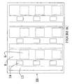
- Another aspect of the invention provides a matrix of electrochemical pixel devices as described above.
- the beneficial process characteristics of the electrochemical pixel device makes it suitable for incorporation in a matrix comprising a plurality of similar or identical pixel devices, in order to form an actively addressed pixel matrix.
- a matrix of pixels exploits the possibility provided by a transistor coupled to a pixel to control the current flows to the colour elements of the pixels.
- a matrix according to this aspect of the invention consists of, for example, three rows and three columns of the novel electrochemical pixel devices described herein, there will be nine electrochromic devices B whose colour may be changed individually. There will also be nine electrochemical transistor devices A to control the current.
- the electrochemical transistor devices A in the pixels forming part of such a matrix may have one or two electrodes for supply of gate voltage to the transistor channel.
- Different characteristics are obtained in the different cases, as explored in further detail below.
- a design having two gate electrodes generally provides for better control of the currents in the matrix system.
- a design of only one gate electrode prevents cross-talk between the second gate electrodes of all the pixels in a row, which may occur as a disadvantage in the two-gate design.
- the one-gate design also makes for fewer crossings of conductors.
- the problem of cross-talk between gate electrodes in a row may also be addressed by the provision of resistances, which prevent the current from a certain pixel from spreading to other pixels in the same row.
- Redox state when reference is made to changes in the "redox state" of the electrochemically active element or electrochromic element, this is intended to include cases where the material in the element is either oxidised or reduced, as well as cases where there is a redistribution of charges within the element, so that one end is reduced and the other end is oxidised. In the latter case, the element as a whole retains its overall redox state, but its redox state has nevertheless been changed according to the definition used herein, due to the internal redistribution of charge carriers.
- colour change when reference is made to “colour change”, this is also meant to include changes in optical density or reflectance, so that “colour change” for example takes into account changes from blue to red, blue to colourless, dark green to light green, grey to white or dark grey to light grey alike.
- the electrochromic polymer is a polymer or copolymer of a 3,4-dialkoxythiophene selected from the group consisting of poly(3,4-methylenedioxythiophene), poly-(3,4-methylenedioxythiophene) derivatives, poly(3,4-ethylenedioxythiophene), poly(3,4-ethylenedioxythiophene) derivatives, poly(3,4-propylenedioxythiophene), poly(3,4-propylenedioxythiophene) derivatives, poly(3,4-butylenedioxythiophene), poly(3,4-butylenedioxythiophene) derivatives, and copolymers therewith.
- a 3,4-dialkoxythiophene selected from the group consisting of poly(3,4-methylenedioxythiophene), poly-(3,4-methylenedioxythiophene) derivatives, poly(3,4-ethylenedioxythiophene), poly(3,4-ethylenedioxythi
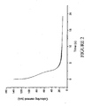
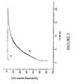
- the electrochemical transistor device was driven by gate voltages between 0 and 1.5 V.
- the electrochemically active element was fully conducting, and at 1.5 V, it was in its "off" state.
- the resistance in the transistor channel was approximately around 10 k ⁇ in its conducting state, which corresponded to a current of 200 ⁇ A at 2 V.
- the resistance was greatly increased.
- Current values of around 200 nA were reached, corresponding to a resistance of 10 M ⁇ .
- the on/off-ratio for the electrochemical transistor device part of the electrochemical pixel device was thus 1000 in this case.
- extreme on/off-ratios of 10 5 in the electrochemical transistor were reached with components made in alternative ways.
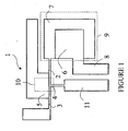
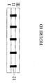
- the middle layer II or spacer layer, is shown in figure 8B .
- This layer comprises the elements of solidified electrolyte that are necessary for the electrochemical reactions in the electrochemical pixel device.
- the electrolyte 9 for the electrochromic device B is provided so that it contacts the electrode 7 of the bottom layer I and the electrochromic element 6 of the top layer III when the layers are put together.
- the electrolyte 10 for the electrochemical transistor device A is provided so that it contacts the electrochemically active element 4 and the gate electrode 5 of the bottom layer when the layers are put together.
- the middle layer II also comprises vias 12, that are formed from an electrically conducting material and serve the purpose of mediating transport of charges to the drain contacts 3 of the bottom layer I from the top layer III, described next.
- Figure 8D is a simple sketch of the three layers taken together, which is primarily intended to illustrate the vias 12, which establish electrical contact between components of layers I and III.
Landscapes
- Physics & Mathematics (AREA)
- Chemical & Material Sciences (AREA)
- Engineering & Computer Science (AREA)
- Nonlinear Science (AREA)
- Optics & Photonics (AREA)
- Nanotechnology (AREA)
- General Physics & Mathematics (AREA)
- Crystallography & Structural Chemistry (AREA)
- Theoretical Computer Science (AREA)
- Mathematical Physics (AREA)
- Materials Engineering (AREA)
- Organic Chemistry (AREA)
- Electrochromic Elements, Electrophoresis, Or Variable Reflection Or Absorption Elements (AREA)
- Devices For Indicating Variable Information By Combining Individual Elements (AREA)
- Thin Film Transistor (AREA)
Applications Claiming Priority (9)
| Application Number | Priority Date | Filing Date | Title |
|---|---|---|---|
| SE0100747A SE521552C2 (sv) | 2001-03-07 | 2001-03-07 | Elektrokromatisk anordning och förfarande för tillverkning av anordningen |
| SE0100747 | 2001-03-07 | ||
| SE0100748A SE520339C2 (sv) | 2001-03-07 | 2001-03-07 | Elektrokemisk transistoranordning och dess tillverkningsförfarande |
| SE0100748 | 2001-03-07 | ||
| US27610501P | 2001-03-16 | 2001-03-16 | |
| US27621801P | 2001-03-16 | 2001-03-16 | |
| US276105P | 2001-03-16 | ||
| US276218P | 2001-03-16 | ||
| PCT/SE2002/000404 WO2002071139A1 (en) | 2001-03-07 | 2002-03-07 | Electrochemical pixel device |
Publications (2)
| Publication Number | Publication Date |
|---|---|
| EP1373976A1 EP1373976A1 (en) | 2004-01-02 |
| EP1373976B1 true EP1373976B1 (en) | 2008-04-23 |
Family
ID=29718695
Family Applications (1)
| Application Number | Title | Priority Date | Filing Date |
|---|---|---|---|
| EP02704001A Expired - Lifetime EP1373976B1 (en) | 2001-03-07 | 2002-03-07 | Electrochemical pixel device |
Country Status (7)
| Country | Link |
|---|---|
| US (1) | US6642069B2 (https=) |
| EP (1) | EP1373976B1 (https=) |
| JP (1) | JP4256163B2 (https=) |
| CN (1) | CN1224862C (https=) |
| AT (1) | ATE393411T1 (https=) |
| DE (1) | DE60226221T2 (https=) |
| WO (1) | WO2002071139A1 (https=) |
Families Citing this family (66)
| Publication number | Priority date | Publication date | Assignee | Title |
|---|---|---|---|---|
| DE10061297C2 (de) | 2000-12-08 | 2003-05-28 | Siemens Ag | Verfahren zur Sturkturierung eines OFETs |
| DE10061299A1 (de) | 2000-12-08 | 2002-06-27 | Siemens Ag | Vorrichtung zur Feststellung und/oder Weiterleitung zumindest eines Umwelteinflusses, Herstellungsverfahren und Verwendung dazu |
| US7034791B1 (en) | 2000-12-14 | 2006-04-25 | Gary Odom | Digital video display employing minimal visual conveyance |
| DE10105914C1 (de) | 2001-02-09 | 2002-10-10 | Siemens Ag | Organischer Feldeffekt-Transistor mit fotostrukturiertem Gate-Dielektrikum und ein Verfahren zu dessen Erzeugung |
| US7012306B2 (en) * | 2001-03-07 | 2006-03-14 | Acreo Ab | Electrochemical device |
| US6756620B2 (en) * | 2001-06-29 | 2004-06-29 | Intel Corporation | Low-voltage and interface damage-free polymer memory device |
| US6624457B2 (en) | 2001-07-20 | 2003-09-23 | Intel Corporation | Stepped structure for a multi-rank, stacked polymer memory device and method of making same |
| DE10151036A1 (de) | 2001-10-16 | 2003-05-08 | Siemens Ag | Isolator für ein organisches Elektronikbauteil |
| DE10151440C1 (de) | 2001-10-18 | 2003-02-06 | Siemens Ag | Organisches Elektronikbauteil, Verfahren zu seiner Herstellung und seine Verwendung |
| DE10160732A1 (de) | 2001-12-11 | 2003-06-26 | Siemens Ag | Organischer Feld-Effekt-Transistor mit verschobener Schwellwertspannung und Verwendung dazu |
| EP1487935A1 (en) * | 2002-03-07 | 2004-12-22 | Acreo AB | Electrochemical device |
| DE10212640B4 (de) | 2002-03-21 | 2004-02-05 | Siemens Ag | Logische Bauteile aus organischen Feldeffekttransistoren |
| ATE355566T1 (de) | 2002-08-23 | 2006-03-15 | Polyic Gmbh & Co Kg | Organisches bauelement zum überspannungsschutz und dazugehörige schaltung |
| DE10253154A1 (de) | 2002-11-14 | 2004-05-27 | Siemens Ag | Messgerät zur Bestimmung eines Analyten in einer Flüssigkeitsprobe |
| US7442954B2 (en) | 2002-11-19 | 2008-10-28 | Polyic Gmbh & Co. Kg | Organic electronic component comprising a patterned, semi-conducting functional layer and a method for producing said component |
| DE10300521A1 (de) * | 2003-01-09 | 2004-07-22 | Siemens Ag | Organoresistiver Speicher |
| DE10302149A1 (de) | 2003-01-21 | 2005-08-25 | Siemens Ag | Verwendung leitfähiger Carbon-black/Graphit-Mischungen für die Herstellung von low-cost Elektronik |
| DE10324388A1 (de) * | 2003-05-28 | 2004-12-30 | Infineon Technologies Ag | Schaltungselement mit einer ersten Schicht aus einem elektrisch isolierenden Substratmaterial und Verfahren zur Herstellung eines Schaltungselements |
| ES2223289B1 (es) * | 2003-08-05 | 2006-04-16 | Fundacion Cidetec | Dispositivo electrocromico basado en polimeros conductores, el procedimiento de obtencion del mismo, asi como el producto obtenido. |
| DE10339036A1 (de) | 2003-08-25 | 2005-03-31 | Siemens Ag | Organisches elektronisches Bauteil mit hochaufgelöster Strukturierung und Herstellungsverfahren dazu |
| US7163734B2 (en) * | 2003-08-26 | 2007-01-16 | Eastman Kodak Company | Patterning of electrically conductive layers by ink printing methods |
| DE10340644B4 (de) | 2003-09-03 | 2010-10-07 | Polyic Gmbh & Co. Kg | Mechanische Steuerelemente für organische Polymerelektronik |
| SE526873C2 (sv) * | 2003-12-02 | 2005-11-15 | Acreo Ab | Vätbarhetsswitch innefattande ett elektrokemiskt aktivt element med växlingsbara ytvätningsegenskaper, förfarande för dess tillverkning samt dess användning i olika tillämpningar |
| US20060138948A1 (en) * | 2004-12-27 | 2006-06-29 | Quantum Paper, Inc. | Addressable and printable emissive display |
| BRPI0519478A2 (pt) * | 2004-12-27 | 2009-02-03 | Quantum Paper Inc | display emissivo endereÇÁvel e imprimÍvel |
| US20060138944A1 (en) * | 2004-12-27 | 2006-06-29 | Quantum Paper | Addressable and printable emissive display |
| DE102005009820A1 (de) | 2005-03-01 | 2006-09-07 | Polyic Gmbh & Co. Kg | Elektronikbaugruppe mit organischen Logik-Schaltelementen |
| JP2006286664A (ja) * | 2005-03-31 | 2006-10-19 | Toshiba Corp | 有機エレクトロルミネッセンス素子 |
| US7443566B2 (en) * | 2006-03-10 | 2008-10-28 | Sony Ericsson Mobile Communications Ab | Low power, configurable display for mobile devices |
| EP1921496A1 (en) * | 2006-11-08 | 2008-05-14 | Acreo AB | Electrochromic device |
| GB0623108D0 (en) * | 2006-11-20 | 2006-12-27 | Sericol Ltd | A printable composition |
| EP1988514A1 (en) * | 2007-05-04 | 2008-11-05 | Acreo AB | Security document circuit |
| US8415879B2 (en) | 2007-05-31 | 2013-04-09 | Nthdegree Technologies Worldwide Inc | Diode for a printable composition |
| US8846457B2 (en) | 2007-05-31 | 2014-09-30 | Nthdegree Technologies Worldwide Inc | Printable composition of a liquid or gel suspension of diodes |
| US8852467B2 (en) | 2007-05-31 | 2014-10-07 | Nthdegree Technologies Worldwide Inc | Method of manufacturing a printable composition of a liquid or gel suspension of diodes |
| US8877101B2 (en) | 2007-05-31 | 2014-11-04 | Nthdegree Technologies Worldwide Inc | Method of manufacturing a light emitting, power generating or other electronic apparatus |
| US9018833B2 (en) | 2007-05-31 | 2015-04-28 | Nthdegree Technologies Worldwide Inc | Apparatus with light emitting or absorbing diodes |
| US8674593B2 (en) | 2007-05-31 | 2014-03-18 | Nthdegree Technologies Worldwide Inc | Diode for a printable composition |
| US9425357B2 (en) | 2007-05-31 | 2016-08-23 | Nthdegree Technologies Worldwide Inc. | Diode for a printable composition |
| US9534772B2 (en) | 2007-05-31 | 2017-01-03 | Nthdegree Technologies Worldwide Inc | Apparatus with light emitting diodes |
| US8384630B2 (en) | 2007-05-31 | 2013-02-26 | Nthdegree Technologies Worldwide Inc | Light emitting, photovoltaic or other electronic apparatus and system |
| US9419179B2 (en) | 2007-05-31 | 2016-08-16 | Nthdegree Technologies Worldwide Inc | Diode for a printable composition |
| US9343593B2 (en) | 2007-05-31 | 2016-05-17 | Nthdegree Technologies Worldwide Inc | Printable composition of a liquid or gel suspension of diodes |
| US8809126B2 (en) | 2007-05-31 | 2014-08-19 | Nthdegree Technologies Worldwide Inc | Printable composition of a liquid or gel suspension of diodes |
| US8889216B2 (en) * | 2007-05-31 | 2014-11-18 | Nthdegree Technologies Worldwide Inc | Method of manufacturing addressable and static electronic displays |
| GB2449928A (en) * | 2007-06-08 | 2008-12-10 | Seiko Epson Corp | Electrochemical thin-film transistor |
| GB2454203A (en) * | 2007-10-30 | 2009-05-06 | Univ Muenster Wilhelms | Time controlled activation of elements |
| US7724499B2 (en) | 2007-11-13 | 2010-05-25 | Industrial Technology Research Institute | Electrolyte transistor |
| US7992332B2 (en) * | 2008-05-13 | 2011-08-09 | Nthdegree Technologies Worldwide Inc. | Apparatuses for providing power for illumination of a display object |
| US8127477B2 (en) | 2008-05-13 | 2012-03-06 | Nthdegree Technologies Worldwide Inc | Illuminating display systems |
| FI20085737L (fi) * | 2008-07-21 | 2010-01-22 | Ronald Oesterbacka | Komponentteja ja piirijärjestelyjä, joissa on ainakin yksi orgaaninen kenttävaikutustransistori |
| US20110170162A1 (en) * | 2008-09-08 | 2011-07-14 | Ntera, Inc. | Printed display systems based on porous substrates |
| EP2414480A4 (en) * | 2009-04-03 | 2012-12-19 | Ciba Geigy Corp | DEVICES CONTAINING COMPOSITIONS COMPRISING CATHODICALLY COLORED ELECTROCHEMICAL POLYMERS AND BINDING POLYMERS |
| CN102576176B (zh) | 2009-10-05 | 2016-08-03 | 阿克里奥瑞典Ict公司 | 电化学装置 |
| SE534488C2 (sv) | 2010-02-22 | 2011-09-06 | Lunavation Ab | Ett system för elektrokinetisk flödesteknik |
| EP2554365A4 (en) * | 2010-03-26 | 2017-08-09 | Tohoku University | Porous structure provided with pattern that is composed of conductive polymer, and method for producing same |
| DE102010026098A1 (de) * | 2010-07-05 | 2012-01-05 | Forschungszentrum Jülich GmbH | Ionisch gesteuertes Dreitorbauelement |
| TW201215980A (en) * | 2010-10-05 | 2012-04-16 | J Touch Corp | Electrochromic module and stereoscopic image display device having the same |
| US9709867B2 (en) | 2010-10-05 | 2017-07-18 | Rise Acreo Ab | Display device |
| JP6035458B2 (ja) | 2011-04-05 | 2016-12-07 | リンテック株式会社 | 電極上での自己整列電解質に基づく電気化学デバイスの製造方法 |
| JP5954412B2 (ja) | 2012-04-23 | 2016-07-20 | 株式会社村田製作所 | 複合材料、アクチュエータおよびそれらの製造方法 |
| JP6054763B2 (ja) * | 2013-02-12 | 2016-12-27 | 株式会社ジャパンディスプレイ | 有機el表示装置 |
| US10312731B2 (en) | 2014-04-24 | 2019-06-04 | Westrock Shared Services, Llc | Powered shelf system for inductively powering electrical components of consumer product packages |
| US20200192171A1 (en) * | 2017-08-23 | 2020-06-18 | National Institute For Materials Science | Electrochromic element and display system using same |
| US10135015B1 (en) * | 2017-11-02 | 2018-11-20 | Palo Alto Research Center Incorporated | Electrochemical clock and oscillator devices |
| US10971765B2 (en) * | 2018-10-05 | 2021-04-06 | Palo Alto Research Center Incorporated | Current control systems and methods |
Family Cites Families (22)
| Publication number | Priority date | Publication date | Assignee | Title |
|---|---|---|---|---|
| DE3721793A1 (de) * | 1986-07-01 | 1988-04-07 | Mitsubishi Electric Corp | Elektrisches element mit verwendung von oxidations-reduktions-substanzen |
| US4993810A (en) | 1989-04-14 | 1991-02-19 | Ford Motor Company | Electrochromic devices comprising metal salts in an ion conductive material |
| US5049868A (en) * | 1989-09-19 | 1991-09-17 | Rockwell International Corporation | Electrochromic display dot drive matrix |
| IT1237269B (it) * | 1989-11-15 | 1993-05-27 | Rete neurale con capacita' di apprendimento per il trattamento di informazioni, e procedimento per il trattamento di informazioni con l'impiego di tale rete. | |
| EP0440957B1 (de) | 1990-02-08 | 1996-03-27 | Bayer Ag | Neue Polythiophen-Dispersionen, ihre Herstellung und ihre Verwendung |
| US5189549A (en) | 1990-02-26 | 1993-02-23 | Molecular Displays, Inc. | Electrochromic, electroluminescent and electrochemiluminescent displays |
| FR2664430B1 (fr) | 1990-07-04 | 1992-09-18 | Centre Nat Rech Scient | Transistor a effet de champ en couche mince de structure mis, dont l'isolant et le semiconducteur sont realises en materiaux organiques. |
| US5138481A (en) | 1991-07-23 | 1992-08-11 | Ford Motor Company | Electrochromic device with color gradient and method of making the device |
| US5413739A (en) | 1992-12-22 | 1995-05-09 | Coleman; James P. | Electrochromic materials and displays |
| US5754329A (en) | 1992-12-22 | 1998-05-19 | Monsanto Company | Electrochromic display laminates |
| WO1994016356A1 (en) * | 1993-01-05 | 1994-07-21 | Martin Marietta Corporation | Improved electrode for display devices |
| FR2746934B1 (fr) * | 1996-03-27 | 1998-05-07 | Saint Gobain Vitrage | Dispositif electrochimique |
| US6369934B1 (en) * | 1996-05-30 | 2002-04-09 | Midwest Research Institute | Self bleaching photoelectrochemical-electrochromic device |
| DE19622600C2 (de) | 1996-06-05 | 2001-08-02 | Fraunhofer Ges Forschung | Elektrochrome Einheit |
| DE19818717A1 (de) * | 1997-04-28 | 1998-10-29 | Wisconsin Label Corp | Elektrochemischer Anzeige- und Zeitmeßmechanismus mit wanderndem Elektrolyt |
| US5877888A (en) | 1997-06-10 | 1999-03-02 | Monsanto Company | Single and double sided electrochromic displays |
| EP0968537B1 (en) * | 1997-08-22 | 2012-05-02 | Creator Technology B.V. | A method of manufacturing a field-effect transistor substantially consisting of organic materials |
| DE19810932A1 (de) * | 1998-03-13 | 1999-09-16 | Bayer Ag | Elektrochrome Anordnung auf Basis von Poly-(3,4-ethylendioxy-thiophen)-Derivaten |
| US6118572A (en) | 1998-07-01 | 2000-09-12 | The Regents Of The University Of California | Photochromic, electrochromic, photoelectrochromic and photovoltaic devices |
| US6506438B2 (en) | 1998-12-15 | 2003-01-14 | E Ink Corporation | Method for printing of transistor arrays on plastic substrates |
| US6387727B1 (en) * | 1999-03-29 | 2002-05-14 | Agere Systems Guardian Corp. | Device comprising n-channel semiconductor material |
| US6444400B1 (en) | 1999-08-23 | 2002-09-03 | Agfa-Gevaert | Method of making an electroconductive pattern on a support |
-
2002
- 2002-03-07 JP JP2002569996A patent/JP4256163B2/ja not_active Expired - Fee Related
- 2002-03-07 WO PCT/SE2002/000404 patent/WO2002071139A1/en not_active Ceased
- 2002-03-07 US US10/091,397 patent/US6642069B2/en not_active Expired - Lifetime
- 2002-03-07 DE DE60226221T patent/DE60226221T2/de not_active Expired - Lifetime
- 2002-03-07 CN CNB028061276A patent/CN1224862C/zh not_active Expired - Fee Related
- 2002-03-07 AT AT02704001T patent/ATE393411T1/de not_active IP Right Cessation
- 2002-03-07 EP EP02704001A patent/EP1373976B1/en not_active Expired - Lifetime
Also Published As
| Publication number | Publication date |
|---|---|
| JP2004522189A (ja) | 2004-07-22 |
| ATE393411T1 (de) | 2008-05-15 |
| EP1373976A1 (en) | 2004-01-02 |
| US6642069B2 (en) | 2003-11-04 |
| WO2002071139A1 (en) | 2002-09-12 |
| US20020134980A1 (en) | 2002-09-26 |
| JP4256163B2 (ja) | 2009-04-22 |
| CN1224862C (zh) | 2005-10-26 |
| DE60226221D1 (de) | 2008-06-05 |
| DE60226221T2 (de) | 2009-05-14 |
| CN1496491A (zh) | 2004-05-12 |
Similar Documents
| Publication | Publication Date | Title |
|---|---|---|
| EP1373976B1 (en) | Electrochemical pixel device | |
| US7301687B2 (en) | Electrochemical device | |
| US6587250B2 (en) | Electrochromic device | |
| US6806511B2 (en) | Electrochemical device | |
| US7489431B2 (en) | Electrochromic device | |
| US9709867B2 (en) | Display device | |
| EP2486447B1 (en) | Electrochemical device | |
| US8564870B2 (en) | Active-matrix electrochromic display device and method for producing the same | |
| WO2012045485A1 (en) | Display device | |
| EP2312386A1 (en) | Passive-matrix electrochromic display device | |
| EP2625565B1 (en) | Passive-matrix electrochromic display device exhibiting a threshold voltage |
Legal Events
| Date | Code | Title | Description |
|---|---|---|---|
| PUAI | Public reference made under article 153(3) epc to a published international application that has entered the european phase |
Free format text: ORIGINAL CODE: 0009012 |
|
| 17P | Request for examination filed |
Effective date: 20030918 |
|
| AK | Designated contracting states |
Kind code of ref document: A1 Designated state(s): AT BE CH CY DE DK ES FI FR GB GR IE IT LI LU MC NL PT SE TR |
|
| AX | Request for extension of the european patent |
Extension state: AL LT LV MK RO SI |
|
| 17Q | First examination report despatched |
Effective date: 20061017 |
|
| GRAP | Despatch of communication of intention to grant a patent |
Free format text: ORIGINAL CODE: EPIDOSNIGR1 |
|
| RIC1 | Information provided on ipc code assigned before grant |
Ipc: G02F 1/155 20060101AFI20071002BHEP |
|
| GRAS | Grant fee paid |
Free format text: ORIGINAL CODE: EPIDOSNIGR3 |
|
| GRAA | (expected) grant |
Free format text: ORIGINAL CODE: 0009210 |
|
| AK | Designated contracting states |
Kind code of ref document: B1 Designated state(s): AT BE CH CY DE DK ES FI FR GB GR IE IT LI LU MC NL PT SE TR |
|
| REG | Reference to a national code |
Ref country code: GB Ref legal event code: FG4D |
|
| REG | Reference to a national code |
Ref country code: CH Ref legal event code: EP |
|
| REF | Corresponds to: |
Ref document number: 60226221 Country of ref document: DE Date of ref document: 20080605 Kind code of ref document: P |
|
| REG | Reference to a national code |
Ref country code: IE Ref legal event code: FG4D Free format text: LANGUAGE OF EP DOCUMENT: FRENCH |
|
| REG | Reference to a national code |
Ref country code: SE Ref legal event code: TRGR |
|
| NLV1 | Nl: lapsed or annulled due to failure to fulfill the requirements of art. 29p and 29m of the patents act | ||
| PG25 | Lapsed in a contracting state [announced via postgrant information from national office to epo] |
Ref country code: PT Free format text: LAPSE BECAUSE OF FAILURE TO SUBMIT A TRANSLATION OF THE DESCRIPTION OR TO PAY THE FEE WITHIN THE PRESCRIBED TIME-LIMIT Effective date: 20080923 Ref country code: ES Free format text: LAPSE BECAUSE OF FAILURE TO SUBMIT A TRANSLATION OF THE DESCRIPTION OR TO PAY THE FEE WITHIN THE PRESCRIBED TIME-LIMIT Effective date: 20080803 Ref country code: FI Free format text: LAPSE BECAUSE OF FAILURE TO SUBMIT A TRANSLATION OF THE DESCRIPTION OR TO PAY THE FEE WITHIN THE PRESCRIBED TIME-LIMIT Effective date: 20080423 Ref country code: NL Free format text: LAPSE BECAUSE OF FAILURE TO SUBMIT A TRANSLATION OF THE DESCRIPTION OR TO PAY THE FEE WITHIN THE PRESCRIBED TIME-LIMIT Effective date: 20080423 |
|
| PG25 | Lapsed in a contracting state [announced via postgrant information from national office to epo] |
Ref country code: AT Free format text: LAPSE BECAUSE OF FAILURE TO SUBMIT A TRANSLATION OF THE DESCRIPTION OR TO PAY THE FEE WITHIN THE PRESCRIBED TIME-LIMIT Effective date: 20080423 |
|
| ET | Fr: translation filed | ||
| PG25 | Lapsed in a contracting state [announced via postgrant information from national office to epo] |
Ref country code: DK Free format text: LAPSE BECAUSE OF FAILURE TO SUBMIT A TRANSLATION OF THE DESCRIPTION OR TO PAY THE FEE WITHIN THE PRESCRIBED TIME-LIMIT Effective date: 20080423 |
|
| PG25 | Lapsed in a contracting state [announced via postgrant information from national office to epo] |
Ref country code: BE Free format text: LAPSE BECAUSE OF FAILURE TO SUBMIT A TRANSLATION OF THE DESCRIPTION OR TO PAY THE FEE WITHIN THE PRESCRIBED TIME-LIMIT Effective date: 20080423 |
|
| PLBE | No opposition filed within time limit |
Free format text: ORIGINAL CODE: 0009261 |
|
| STAA | Information on the status of an ep patent application or granted ep patent |
Free format text: STATUS: NO OPPOSITION FILED WITHIN TIME LIMIT |
|
| 26N | No opposition filed |
Effective date: 20090126 |
|
| PG25 | Lapsed in a contracting state [announced via postgrant information from national office to epo] |
Ref country code: IT Free format text: LAPSE BECAUSE OF FAILURE TO SUBMIT A TRANSLATION OF THE DESCRIPTION OR TO PAY THE FEE WITHIN THE PRESCRIBED TIME-LIMIT Effective date: 20080423 |
|
| PG25 | Lapsed in a contracting state [announced via postgrant information from national office to epo] |
Ref country code: MC Free format text: LAPSE BECAUSE OF NON-PAYMENT OF DUE FEES Effective date: 20090331 |
|
| REG | Reference to a national code |
Ref country code: CH Ref legal event code: PL |
|
| REG | Reference to a national code |
Ref country code: IE Ref legal event code: MM4A |
|
| PG25 | Lapsed in a contracting state [announced via postgrant information from national office to epo] |
Ref country code: LI Free format text: LAPSE BECAUSE OF NON-PAYMENT OF DUE FEES Effective date: 20090331 Ref country code: IE Free format text: LAPSE BECAUSE OF NON-PAYMENT OF DUE FEES Effective date: 20090307 Ref country code: CH Free format text: LAPSE BECAUSE OF NON-PAYMENT OF DUE FEES Effective date: 20090331 |
|
| PG25 | Lapsed in a contracting state [announced via postgrant information from national office to epo] |
Ref country code: GR Free format text: LAPSE BECAUSE OF FAILURE TO SUBMIT A TRANSLATION OF THE DESCRIPTION OR TO PAY THE FEE WITHIN THE PRESCRIBED TIME-LIMIT Effective date: 20080724 |
|
| PG25 | Lapsed in a contracting state [announced via postgrant information from national office to epo] |
Ref country code: LU Free format text: LAPSE BECAUSE OF NON-PAYMENT OF DUE FEES Effective date: 20090307 |
|
| PG25 | Lapsed in a contracting state [announced via postgrant information from national office to epo] |
Ref country code: TR Free format text: LAPSE BECAUSE OF FAILURE TO SUBMIT A TRANSLATION OF THE DESCRIPTION OR TO PAY THE FEE WITHIN THE PRESCRIBED TIME-LIMIT Effective date: 20080423 |
|
| PG25 | Lapsed in a contracting state [announced via postgrant information from national office to epo] |
Ref country code: CY Free format text: LAPSE BECAUSE OF FAILURE TO SUBMIT A TRANSLATION OF THE DESCRIPTION OR TO PAY THE FEE WITHIN THE PRESCRIBED TIME-LIMIT Effective date: 20080423 |
|
| PGFP | Annual fee paid to national office [announced via postgrant information from national office to epo] |
Ref country code: SE Payment date: 20150318 Year of fee payment: 14 |
|
| REG | Reference to a national code |
Ref country code: FR Ref legal event code: PLFP Year of fee payment: 15 |
|
| REG | Reference to a national code |
Ref country code: SE Ref legal event code: EUG |
|
| PG25 | Lapsed in a contracting state [announced via postgrant information from national office to epo] |
Ref country code: SE Free format text: LAPSE BECAUSE OF NON-PAYMENT OF DUE FEES Effective date: 20160308 |
|
| REG | Reference to a national code |
Ref country code: FR Ref legal event code: PLFP Year of fee payment: 16 |
|
| REG | Reference to a national code |
Ref country code: FR Ref legal event code: PLFP Year of fee payment: 17 |
|
| PGFP | Annual fee paid to national office [announced via postgrant information from national office to epo] |
Ref country code: DE Payment date: 20190219 Year of fee payment: 18 Ref country code: GB Payment date: 20190225 Year of fee payment: 18 |
|
| PGFP | Annual fee paid to national office [announced via postgrant information from national office to epo] |
Ref country code: FR Payment date: 20190218 Year of fee payment: 18 |
|
| REG | Reference to a national code |
Ref country code: DE Ref legal event code: R119 Ref document number: 60226221 Country of ref document: DE |
|
| PG25 | Lapsed in a contracting state [announced via postgrant information from national office to epo] |
Ref country code: FR Free format text: LAPSE BECAUSE OF NON-PAYMENT OF DUE FEES Effective date: 20200331 Ref country code: DE Free format text: LAPSE BECAUSE OF NON-PAYMENT OF DUE FEES Effective date: 20201001 |
|
| GBPC | Gb: european patent ceased through non-payment of renewal fee |
Effective date: 20200307 |
|
| PG25 | Lapsed in a contracting state [announced via postgrant information from national office to epo] |
Ref country code: GB Free format text: LAPSE BECAUSE OF NON-PAYMENT OF DUE FEES Effective date: 20200307 |