EP1372010A2 - Verfahren zur Herstellung eines optischen Elements - Google Patents
Verfahren zur Herstellung eines optischen Elements Download PDFInfo
- Publication number
- EP1372010A2 EP1372010A2 EP03013247A EP03013247A EP1372010A2 EP 1372010 A2 EP1372010 A2 EP 1372010A2 EP 03013247 A EP03013247 A EP 03013247A EP 03013247 A EP03013247 A EP 03013247A EP 1372010 A2 EP1372010 A2 EP 1372010A2
- Authority
- EP
- European Patent Office
- Prior art keywords
- polishing
- manufacturing
- optical element
- caf
- altered layer
- Prior art date
- Legal status (The legal status is an assumption and is not a legal conclusion. Google has not performed a legal analysis and makes no representation as to the accuracy of the status listed.)
- Withdrawn
Links
- 230000003287 optical effect Effects 0.000 title claims abstract description 95
- 238000000034 method Methods 0.000 title claims abstract description 41
- 238000004519 manufacturing process Methods 0.000 title claims abstract description 32
- 238000005498 polishing Methods 0.000 claims abstract description 98
- 239000000758 substrate Substances 0.000 claims abstract description 42
- 238000004140 cleaning Methods 0.000 claims abstract description 25
- 238000009832 plasma treatment Methods 0.000 claims abstract description 21
- 238000004544 sputter deposition Methods 0.000 claims abstract description 11
- WUKWITHWXAAZEY-UHFFFAOYSA-L calcium difluoride Chemical compound [F-].[F-].[Ca+2] WUKWITHWXAAZEY-UHFFFAOYSA-L 0.000 claims description 45
- 229910001634 calcium fluoride Inorganic materials 0.000 claims description 45
- 239000004065 semiconductor Substances 0.000 claims description 11
- 230000007423 decrease Effects 0.000 claims description 8
- 239000010409 thin film Substances 0.000 claims description 7
- 238000005286 illumination Methods 0.000 claims description 6
- 239000011368 organic material Substances 0.000 claims description 3
- 230000005465 channeling Effects 0.000 claims description 2
- 238000005259 measurement Methods 0.000 claims description 2
- 230000015556 catabolic process Effects 0.000 abstract description 7
- 238000006731 degradation reaction Methods 0.000 abstract description 7
- 230000001747 exhibiting effect Effects 0.000 abstract description 2
- 229910004261 CaF 2 Inorganic materials 0.000 abstract 4
- 239000010410 layer Substances 0.000 description 64
- 230000006378 damage Effects 0.000 description 21
- 230000003247 decreasing effect Effects 0.000 description 16
- 238000002834 transmittance Methods 0.000 description 15
- 239000010408 film Substances 0.000 description 11
- 239000002245 particle Substances 0.000 description 11
- 239000006061 abrasive grain Substances 0.000 description 10
- 230000008569 process Effects 0.000 description 8
- 239000000463 material Substances 0.000 description 7
- 230000015572 biosynthetic process Effects 0.000 description 6
- 230000003746 surface roughness Effects 0.000 description 6
- 238000010521 absorption reaction Methods 0.000 description 4
- 230000007547 defect Effects 0.000 description 4
- 230000007613 environmental effect Effects 0.000 description 4
- 239000013078 crystal Substances 0.000 description 3
- 239000002994 raw material Substances 0.000 description 3
- 238000000151 deposition Methods 0.000 description 2
- 238000013461 design Methods 0.000 description 2
- 238000011161 development Methods 0.000 description 2
- 238000005530 etching Methods 0.000 description 2
- 125000001153 fluoro group Chemical group F* 0.000 description 2
- 239000012634 fragment Substances 0.000 description 2
- 238000007689 inspection Methods 0.000 description 2
- 238000012986 modification Methods 0.000 description 2
- 230000004048 modification Effects 0.000 description 2
- 238000005001 rutherford backscattering spectroscopy Methods 0.000 description 2
- 239000000243 solution Substances 0.000 description 2
- 238000012360 testing method Methods 0.000 description 2
- 238000001771 vacuum deposition Methods 0.000 description 2
- 230000002378 acidificating effect Effects 0.000 description 1
- 239000012670 alkaline solution Substances 0.000 description 1
- 125000004429 atom Chemical group 0.000 description 1
- 230000008021 deposition Effects 0.000 description 1
- 238000010586 diagram Methods 0.000 description 1
- 238000010494 dissociation reaction Methods 0.000 description 1
- 230000005593 dissociations Effects 0.000 description 1
- 230000000694 effects Effects 0.000 description 1
- 238000005538 encapsulation Methods 0.000 description 1
- 239000011521 glass Substances 0.000 description 1
- 230000003993 interaction Effects 0.000 description 1
- 238000005468 ion implantation Methods 0.000 description 1
- 150000002500 ions Chemical class 0.000 description 1
- 239000004973 liquid crystal related substance Substances 0.000 description 1
- 238000001459 lithography Methods 0.000 description 1
- 230000003647 oxidation Effects 0.000 description 1
- 238000007254 oxidation reaction Methods 0.000 description 1
- 238000004806 packaging method and process Methods 0.000 description 1
- 239000000843 powder Substances 0.000 description 1
- 238000011160 research Methods 0.000 description 1
- 229910052710 silicon Inorganic materials 0.000 description 1
- 239000010703 silicon Substances 0.000 description 1
- 239000002344 surface layer Substances 0.000 description 1
Images





Classifications
-
- C—CHEMISTRY; METALLURGY
- C30—CRYSTAL GROWTH
- C30B—SINGLE-CRYSTAL GROWTH; UNIDIRECTIONAL SOLIDIFICATION OF EUTECTIC MATERIAL OR UNIDIRECTIONAL DEMIXING OF EUTECTOID MATERIAL; REFINING BY ZONE-MELTING OF MATERIAL; PRODUCTION OF A HOMOGENEOUS POLYCRYSTALLINE MATERIAL WITH DEFINED STRUCTURE; SINGLE CRYSTALS OR HOMOGENEOUS POLYCRYSTALLINE MATERIAL WITH DEFINED STRUCTURE; AFTER-TREATMENT OF SINGLE CRYSTALS OR A HOMOGENEOUS POLYCRYSTALLINE MATERIAL WITH DEFINED STRUCTURE; APPARATUS THEREFOR
- C30B33/00—After-treatment of single crystals or homogeneous polycrystalline material with defined structure
-
- C—CHEMISTRY; METALLURGY
- C30—CRYSTAL GROWTH
- C30B—SINGLE-CRYSTAL GROWTH; UNIDIRECTIONAL SOLIDIFICATION OF EUTECTIC MATERIAL OR UNIDIRECTIONAL DEMIXING OF EUTECTOID MATERIAL; REFINING BY ZONE-MELTING OF MATERIAL; PRODUCTION OF A HOMOGENEOUS POLYCRYSTALLINE MATERIAL WITH DEFINED STRUCTURE; SINGLE CRYSTALS OR HOMOGENEOUS POLYCRYSTALLINE MATERIAL WITH DEFINED STRUCTURE; AFTER-TREATMENT OF SINGLE CRYSTALS OR A HOMOGENEOUS POLYCRYSTALLINE MATERIAL WITH DEFINED STRUCTURE; APPARATUS THEREFOR
- C30B29/00—Single crystals or homogeneous polycrystalline material with defined structure characterised by the material or by their shape
- C30B29/10—Inorganic compounds or compositions
- C30B29/12—Halides
Definitions
- the present invention relates to methods for manufacturing optical elements, and more particularly, relates to a method for manufacturing an optical element formed of a CaF 2 material having resistance against plasma damage.
- CaF 2 is a necessary and essential material for forming optical elements used in a vacuum ultraviolet region.
- the optical elements formed of a CaF 2 material have been used in various optical devices such as a semiconductor exposure apparatus and a broadcasting camera.
- Optical elements are manufactured by polishing, cleaning, and film-forming steps, as shown in Fig. 10. After a raw material primarily composed of CaF 2 for an optical element is polished to form a desired shape in the polishing step, fragments of an abrasive powder and organic materials adhered to the CaF 2 are then removed in the cleaning step, and in the film-forming step, an optical thin film such as an antireflection film is formed on a surface of the CaF 2 substrate.
- the cleaning method performed in the cleaning step for example, there may be mentioned ultraviolet cleaning using ultraviolet rays or plasma cleaning using plasma.
- the cleaning time can be significantly decreased.
- the film-forming method As a film-forming method used in the film-forming step, vacuum deposition, sputtering, or the like may be mentioned. In the case of sputtering using plasma, compared to the case of vacuum deposition, the film thus formed has a high film density, and an optical thin film having superior laser and environment resistance can be formed.
- the plasma damage means the cause of optical loss which is generated by bombardment of charged particles onto a CaF 2 substrate when treatment (hereinafter referred to as "plasma treatment") generating plasma, such as plasma cleaning or sputtering, is performed in a chamber in which the CaF 2 substrate is placed.
- plasma treatment plasma treatment generating plasma, such as plasma cleaning or sputtering
- the cleaning time can be significantly decreased, or an optical thin film having superior laser or environmental resistance can be formed.
- a problem may arise in that the transmittance of the element thus formed is decreased by plasma damage.
- Fig. 11 shows the difference in transmittance of a plasma-damaged CaF 2 substrate from that of a CaF 2 substrate free from plasma damage as optical loss (ratio of decrease in transmittance).
- the horizontal axis indicates wavelengths
- the vertical axis indicates values obtained by deducting the transmittance of a CaF 2 substrate which is processed with plasma treatment from that of a CaF 2 substrate which is not processed therewith. That is, this value of the optical loss represents the decrease in transmittance of the CaF 2 substrate caused by plasma treatment.
- the optical loss caused by plasma damage depends on output power of plasma or time exposed thereto; however, in a visible region of a wavelength from 350 to 800 nm and a vacuum ultraviolet region of a wavelength of 250 nm or less, the optical loss becomes serious.
- An object of the present invention is to provide a method for manufacturing an optical element using CaF 2 as a raw material, in which even when plasma treatment is performed, degradation of optical properties of the optical element caused by plasma damage can be avoided or suppressed.
- a method for manufacturing an optical element comprises the steps of polishing a CaF 2 substrate so that a process-altered layer formed by the polishing has a thickness of 30 nm or less, and performing plasma treatment in a chamber in which the polished CaF 2 substrate is placed.
- Fig. 1 is a block diagram showing the present invention.
- Figs. 2A to 2C are views showing the state in which a process-altered layer is generated in a polishing step.
- Fig. 3 is a graph showing the relationship between the time for finish polishing and the thickness of a remaining process-altered layer.
- Fig. 4 is a graph showing the relationship between a process-altered layer and the optical property in a wavelength region of 185 to 215 nm of an optical element provided with an antireflection film.
- Fig. 5 is a graph showing the relationship between the thickness of a process-altered layer and the amount of optical loss caused by plasma damage.
- Fig. 6 is a graph showing the relationship between a process-altered layer and the optical property in a wavelength region of 300 to 800 nm of an optical element provided with an antireflection film.
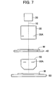
- Fig. 7 is a view showing a projection type exposure apparatus having an optical system composed of CaF 2 used as a lens.
- Fig. 8 is a chart showing a process for manufacturing a device.
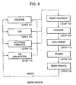
- Fig. 9 is a view showing the wafer process shown in Fig. 8.
- Fig. 10 is a view showing a process for manufacturing an optical element.
- Fig. 11 is a view showing the relationship between the optical loss and the wavelength.
- the bonding strength between atoms is decreased, and hence fluorine atoms are easily dissociated from the CaF 2 by bombardment of charged particles in plasma.
- the lattice defects generated by the dissociation of fluorine atoms form an absorption band called a color center by the interaction with electrons present in plasma, and hence the optical loss is caused primarily thereby.
- the process-altered layer itself does not cause an optical loss; however, when the process-altered layer is bombarded with charged particles in plasma, the optical loss is caused thereby. Hence, in order to reduce the plasma damage, the thickness of the process-altered layer is removed to the level at which the optical loss does not occur.
- a schematic view of the present invention is shown in Fig. 1.
- the CaF 2 substrate is polished in a polishing step.
- a process-altered layer is generated on a surface of the substrate, and the polishing is performed so that the thickness of the process-altered layer is 30 nm or less.
- an optical thin film is formed on a surface of the substrate in a film-forming step, and at this stage, plasma treatment is performed in one of the cleaning step and the film forming step or is performed in both steps.
- the cleaning time can be significantly decreased, and when sputtering film formation is performed in the film-forming step, an optical thin film having superior laser resistance and environmental resistance can be formed.
- both effects described above can be obtained.
- the thickness of the process-altered layer is decreased to 30 nm or less in the polishing step, even when plasma treatment is performed, degradation of optical properties caused thereby can be suppressed (the reason the thickness of the process-altered layer is decreased to 30 nm or less will be described later).
- the polishing step performs polishing at least twice under different conditions.
- the conditions mentioned above include a particle diameter of abrasive grains, a polishing speed, a pressure applied onto an element surface, and the like.
- the particle diameter of abrasive grains and the pressure applied onto the element surface are preferably decreased.
- the process-altered layer is generated; however, the thickness thereof depends on the particle diameter of the abrasive grains and the pressure applied onto the element surface.
- the particle diameter of the abrasive grains is large and the pressure applied onto the element surface is high, a thick process-altered layer is formed, and on the other hand, when the particle diameter of the abrasive grains is small and the pressure applied onto the element surface is low, a thin process-altered layer is formed.
- Fig. 2A is a view showing a CaF 2 substrate before polishing.
- first polishing in order to polish the CaF 2 substrate in a large amount, abrasive particles having a large particle diameter is used and the pressure applied onto the element surface is increased.
- the polishing amount is increased; however, at the same time, the process-altered layer formed on the CaF 2 surface has a large thickness.
- finish polishing which is the last polishing, is performed. In this polishing, the particle diameter of the abrasive grains is small, and the pressure applied onto the element surface is low.
- the polishing amount by the finish polishing is small, and the thickness of the process-altered layer generated in the finish polishing is small.
- Fig. 2C the CaF 2 substrate after finish polishing is shown.
- a material polished in the finish polishing is part of the process-altered layer formed in the polishing before the finish polishing. That is, the primary reason the process-altered layer is present in the optical element after the polishing step is that the process-altered layer is formed in polishing performed before the finish polishing, which is the last polishing, and dominates over the process-altered layer formed in the finish polishing.
- the surface roughness of the CaF 2 after the finish polishing is approximately several angstroms and is sufficient for a practical use. Since being performed for decreasing the surface roughness, in the past, the finish polishing is stopped when the surface roughness reaches a predetermined standard value or less, and the polishing amount has not been regarded as a problem. In addition, it has not been known at all that the process-altered layer processed by plasma treatment causes the degradation of the optical properties. Hence, although a CaF 2 substrate processed by a conventional polishing step had a sufficient surface roughness for a practical use, a process-altered layer having a large thickness remains in the substrate.
- the process-altered layer formed prior to the finish polishing is polished in the step thereof so that the thickness of the process-altered layer is decreased, and as a result, a CaF 2 substrate having resistance against plasma treatment can be realized.
- the process-altered layer is naturally formed also in the finish polishing, the thickness thereof is significantly smaller than that formed by polishing performed before the finish polishing. Accordingly, the process-altered layer is removed in the finish polishing until the thickness of the remaining layer becomes equivalent to that formed in the finish polishing. The thickness thus obtained is the minimum thickness of the process-altered layer.
- the minimum thickness of the process-altered layer depends on finish polishing methods.
- finish polishing method for example, there may be mentioned pitch-polishing, electro-rheological polishing, and magneto-rheological polishing.
- the thickness of the process-altered layer can be 15 nm or less, and hence the above two polishing methods are superior as the finish polishing method.
- the thickness of the process-altered layer can always be minimum; however, in the case described above, since the polishing amount is small, and a tremendous long period of time is required for polishing, this case cannot be practically performed.
- the process-altered layer When being immersed in a solution such as an aqueous, an acidic, or an alkaline solution, the process-altered layer can be removed.
- a solution such as an aqueous, an acidic, or an alkaline solution
- the substrate surface after the process-altered layer is removed is roughened so as not to meet the standard value of the surface roughness, and as a result, after the removal of the process-altered layer, the finish polishing must be performed.
- the process becomes complicated since a step of immersing the substrate into the solution must be additionally performed.
- a high quality optical element can be obtained suppressing degradation of the optical properties in plasma treatment, which is generally caused by plasma damage.
- the optical element according to the manufacturing method of the present invention which is formed by the steps of polishing CaF 2 , performing plasma cleaning, and then depositing an optical thin film on the surface of CaF 2 by sputtering, can be cleaned in a short period of time and has superior laser resistance and environmental resistance. Accordingly, a semiconductor exposure apparatus comprising an optical system formed of this optical element has superior laser resistance and environmental resistance.
- the polishing amount of the process-altered layer depends on a polishing time for the finish polishing.
- Fig. 3 is a graph showing the relationship between the polishing time for the finish polishing of CaF 2 and the thickness of the remaining process-altered layer when a magneto-rheological polishing method is used as the finish polishing method.
- the thickness of the process-altered layer was identified by RBS (Rutherford Backscattering Spectrometry) channeling measurement.
- the thickness of the remaining process-altered layer was decreased to approximately 15 nm or less as the polishing time was increased up to approximately 60 seconds; however, subsequently, the thickness of the process-altered layer was not so much changed even when the polishing time was further increased.
- the reason for this is that the thickness of the process-altered layer reached to the minimum value at a polishing time of approximately 60 seconds. That is, even when some allowance for the polishing time is taken into consideration, the finish polishing performed for approximately up to 100 seconds may be sufficient.
- the thickness of the process-altered layer can be controlled by the polishing time.
- sample B having a process-altered layer 30 nm thick the decrease in transmittance (increase in absorption by the substrate) caused by plasma damage was 0.7% at a wavelength of 193 nm.
- sample C having a process-altered layer 50 nm thick the decrease in transmittance (increase in absorption by the substrate) caused by plasma damage was 7.2%, and the substrate after the film formation was colored in blue.
- sample A having a process-altered layer 15 nm thick the decrease in transmittance (increase in absorption by the substrate) caused by plasma damage was not observed, and as an optical element, superior properties were obtained.
- Fig. 5 shows the relationship between the thickness of the process-altered layer and the optical loss at a wavelength of 193 nm caused by plasma damage generated in the film-forming step.
- the thickness of the process-altered layer is 50 nm which is equivalent to that obtained by the conventional finish polishing
- the optical loss is decreased. That is, as the thickness of the process-altered layer is decreased, the optical loss caused by plasma damage is decreased, and then it is understood that the removal of the process-altered layer is effective to suppress the optical loss caused by plasma damage.
- the optical loss caused by plasma damage can also be suppressed.
- Fig. 6 the transmittance at a wavelength of 300 to 800 nm is shown.
- the thickness of the process-altered layer is 50 nm
- the decrease in transmittance at around a wavelength of approximately 550 nm is significant; however, when the thickness is progressively decreased to 30 nm and 15 nm, the transmittance is increased, and in addition, an approximately uniform transmittance can be obtained in the entire visible region. This phenomenon is advantageous since an optical element having uniform properties in the entire visible region can be formed.
- reference numeral 10 indicates an optical axis
- numeral 20 a light source generating light having a wavelength of 157 nm in a vacuum UV region
- numeral 30 an illumination optical system provided with an aperture stop 30A
- numeral 40 a stage on which a reticle M is placed
- numeral 50 a projection optical system provided with an aperture stop 50A
- numeral 60 a stage on which a wafer W is placed.
- the reticle M is irradiated with light emitted from the light source 20 through the illumination optical system 30, and an image of a device pattern of the reticle M is projected onto the wafer W by the projection optical system 50.
- the optical system is formed of a lens, made of CaF 2 used as a glass material, manufactured by the manufacturing method of the embodiment according to the present invention. Since the optical system is formed using the lens described above, even for light having a wavelength of 157 nm, superior transmittance can be realized.
- Fig. 8 shows a manufacturing flow of a semiconductor ' device (a semiconductor device such as an IC or an LSI, a liquid crystal panel, a CCD, or the like).
- Step 1 circuit design
- Step 2 mask formation
- Step 3 wafer manufacturing
- Step 4 wafer process
- a front-end process by using the mask and the wafer thus prepared, an actual circuit is formed on the wafer by a lithography technique.
- Step 5 assembly
- Step 6 inspection
- operation test endurance test
- Step 7 shipment
- Step 11 oxidation
- Step 12 an insulating film is formed on the surface of the wafer.
- Step 13 electrode formation
- Step 14 ion implantation
- ions are implanted into the wafer.
- Step 15 resist treatment
- Step 16 exposure
- Step 17 development
- Step 18 etching
- Step 19 resist removal
- a method for manufacturing an optical element formed of CaF 2 is provided, the optical element exhibiting a small optical loss even when being processed with plasma treatment such as sputtering or plasma cleaning.
- the method for manufacturing an optical element, described above has the steps of polishing a CaF 2 substrate and performing plasma treatment, such as sputtering or plasma cleaning, in a chamber in which the polished CaF 2 substrate is placed.
- the thickness of a process-altered layer formed on a surface of the CaF 2 substrate is polished so as to be 30 nm or less, and hence there is provided a method for manufacturing an optical element capable of preventing degradation of the optical properties caused by plasma treatment.
Landscapes
- Chemical & Material Sciences (AREA)
- Engineering & Computer Science (AREA)
- Crystallography & Structural Chemistry (AREA)
- Materials Engineering (AREA)
- Metallurgy (AREA)
- Organic Chemistry (AREA)
- Inorganic Chemistry (AREA)
- Exposure And Positioning Against Photoresist Photosensitive Materials (AREA)
- Surface Treatment Of Optical Elements (AREA)
- Cleaning In General (AREA)
- Exposure Of Semiconductors, Excluding Electron Or Ion Beam Exposure (AREA)
- Surface Treatment Of Glass (AREA)
Applications Claiming Priority (2)
| Application Number | Priority Date | Filing Date | Title |
|---|---|---|---|
| JP2002172781 | 2002-06-13 | ||
| JP2002172781A JP2004020710A (ja) | 2002-06-13 | 2002-06-13 | 光学素子の製造方法 |
Publications (2)
| Publication Number | Publication Date |
|---|---|
| EP1372010A2 true EP1372010A2 (de) | 2003-12-17 |
| EP1372010A3 EP1372010A3 (de) | 2008-04-16 |
Family
ID=29561795
Family Applications (1)
| Application Number | Title | Priority Date | Filing Date |
|---|---|---|---|
| EP03013247A Withdrawn EP1372010A3 (de) | 2002-06-13 | 2003-06-12 | Verfahren zur Herstellung eines optischen Elements |
Country Status (3)
| Country | Link |
|---|---|
| US (1) | US6835661B2 (de) |
| EP (1) | EP1372010A3 (de) |
| JP (1) | JP2004020710A (de) |
Cited By (4)
| Publication number | Priority date | Publication date | Assignee | Title |
|---|---|---|---|---|
| WO2009017634A3 (en) * | 2007-07-31 | 2010-03-04 | Corning Incorporated | Cleaning method for duv optical elements to extend their lifetime |
| CN105269412A (zh) * | 2015-09-17 | 2016-01-27 | 中国科学院光电技术研究所 | 一种适用于氟化钙凸锥镜高效加工的联合工艺方法 |
| CN106271901A (zh) * | 2016-09-22 | 2017-01-04 | 中国科学院光电技术研究所 | 一种适用于氟化钙凹锥镜高效加工的联合工艺方法 |
| CN106826409A (zh) * | 2017-02-09 | 2017-06-13 | 同济大学 | 一种基于铝盐络合物的氟化钙单晶抛光方法 |
Family Cites Families (5)
| Publication number | Priority date | Publication date | Assignee | Title |
|---|---|---|---|---|
| US6835505B2 (en) * | 1998-10-08 | 2004-12-28 | Rochester Institute Of Technology | Mask for projection photolithography at or below about 160 nm and a method thereof |
| US6595834B2 (en) * | 1999-06-25 | 2003-07-22 | Corning Incorporated | Method of making <200nm light transmitting optical fluoride crystals for transmitting less than 200nm light |
| KR20020036789A (ko) * | 1999-06-25 | 2002-05-16 | 알프레드 엘. 미첼슨 | 세륨 옥사이드를 이용한 마이크로리소그라피용 플로라이드결정 광학 렌즈 및 예형의 연마방법 |
| JP2001201608A (ja) | 1999-11-08 | 2001-07-27 | Nikon Corp | 光学薄膜の成膜方法、光学素子及び露光装置 |
| JP2002082211A (ja) * | 2000-06-08 | 2002-03-22 | Canon Inc | 光学素子の製造方法 |
-
2002
- 2002-06-13 JP JP2002172781A patent/JP2004020710A/ja active Pending
-
2003
- 2003-05-30 US US10/448,285 patent/US6835661B2/en not_active Expired - Lifetime
- 2003-06-12 EP EP03013247A patent/EP1372010A3/de not_active Withdrawn
Cited By (6)
| Publication number | Priority date | Publication date | Assignee | Title |
|---|---|---|---|---|
| WO2009017634A3 (en) * | 2007-07-31 | 2010-03-04 | Corning Incorporated | Cleaning method for duv optical elements to extend their lifetime |
| CN105269412A (zh) * | 2015-09-17 | 2016-01-27 | 中国科学院光电技术研究所 | 一种适用于氟化钙凸锥镜高效加工的联合工艺方法 |
| CN106271901A (zh) * | 2016-09-22 | 2017-01-04 | 中国科学院光电技术研究所 | 一种适用于氟化钙凹锥镜高效加工的联合工艺方法 |
| CN106271901B (zh) * | 2016-09-22 | 2018-06-01 | 中国科学院光电技术研究所 | 一种适用于氟化钙凹锥镜高效加工的联合工艺方法 |
| CN106826409A (zh) * | 2017-02-09 | 2017-06-13 | 同济大学 | 一种基于铝盐络合物的氟化钙单晶抛光方法 |
| CN106826409B (zh) * | 2017-02-09 | 2018-05-08 | 同济大学 | 一种基于铝盐络合物的氟化钙单晶抛光方法 |
Also Published As
| Publication number | Publication date |
|---|---|
| US20030231416A1 (en) | 2003-12-18 |
| US6835661B2 (en) | 2004-12-28 |
| JP2004020710A (ja) | 2004-01-22 |
| EP1372010A3 (de) | 2008-04-16 |
Similar Documents
| Publication | Publication Date | Title |
|---|---|---|
| US6660546B2 (en) | Method of etching an object, method of repairing pattern, nitride pattern and semiconductor device | |
| KR101704846B1 (ko) | 세정용 레티클, 레티클 스테이지의 세정 방법 및 반도체 장치의 제조 방법 | |
| KR102060035B1 (ko) | 평탄화된 극자외선 리소그래피 블랭크, 및 그를 위한 제조 및 리소그래피 시스템들 | |
| US9195148B2 (en) | Side seal for wet lens elements | |
| US7763399B2 (en) | Removal of ionic residues or oxides and prevention of photo-induced defects, ionic crystal or oxide growth on photolithographic surfaces | |
| US7767365B2 (en) | Methods for forming and cleaning photolithography reticles | |
| US5942760A (en) | Method of forming a semiconductor device utilizing scalpel mask, and mask therefor | |
| US6040118A (en) | Critical dimension equalization across the field by second blanket exposure at low dose over bleachable resist | |
| US8439728B2 (en) | Reticle carrier | |
| US6835661B2 (en) | Method for manufacturing optical element | |
| JP7407871B2 (ja) | ブランクマスク用基板の洗浄方法、ブランクマスク用基板及びそれを含むブランクマスク | |
| CN115755516A (zh) | 空白掩模、使用其的光掩模及半导体器件的制造方法 | |
| JP4006341B2 (ja) | 光学素子の洗浄装置及び方法 | |
| EP1292864B1 (de) | Verfahren zur verringerung von entwicklungsdefekten in und um öffnungen in photolack mittels mehrfacher entwickler/spülzyklen | |
| US8148054B2 (en) | Immersion multiple-exposure method and immersion exposure system for separately performing multiple exposure of micropatterns and non-micropatterns | |
| US6555234B1 (en) | Barrier for and a method of reducing outgassing from a photoresist material | |
| US6481119B1 (en) | Apparatus for removing organic antireflection coating | |
| JP2006516052A (ja) | 炭素層を有する透過マスクを用いてウエハ上にフォトレジストをパターンニングする方法 | |
| KR102893004B1 (ko) | 심자외 광원용 광학 컴포넌트 | |
| US6291135B1 (en) | Ionization technique to reduce defects on next generation lithography mask during exposure | |
| JP2001028330A (ja) | 露光マスク、露光方法、及び露光マスクの製造方法 | |
| JP2004029418A (ja) | 光学素子の製造方法 | |
| JP2006088128A (ja) | 洗浄方法、洗浄装置、露光装置、及びデバイス製造方法 | |
| Shim et al. | Improved characteristics of rainbow defects with novel wafer edge exposure technique | |
| KR20070022978A (ko) | 포토리소그래피 장치 |
Legal Events
| Date | Code | Title | Description |
|---|---|---|---|
| PUAI | Public reference made under article 153(3) epc to a published international application that has entered the european phase |
Free format text: ORIGINAL CODE: 0009012 |
|
| 17P | Request for examination filed |
Effective date: 20030612 |
|
| AK | Designated contracting states |
Kind code of ref document: A2 Designated state(s): AT BE BG CH CY CZ DE DK EE ES FI FR GB GR HU IE IT LI LU MC NL PT RO SE SI SK TR |
|
| AX | Request for extension of the european patent |
Extension state: AL LT LV MK |
|
| PUAL | Search report despatched |
Free format text: ORIGINAL CODE: 0009013 |
|
| AK | Designated contracting states |
Kind code of ref document: A3 Designated state(s): AT BE BG CH CY CZ DE DK EE ES FI FR GB GR HU IE IT LI LU MC NL PT RO SE SI SK TR |
|
| AX | Request for extension of the european patent |
Extension state: AL LT LV MK |
|
| AKX | Designation fees paid |
Designated state(s): DE NL |
|
| 17Q | First examination report despatched |
Effective date: 20090529 |
|
| STAA | Information on the status of an ep patent application or granted ep patent |
Free format text: STATUS: THE APPLICATION HAS BEEN WITHDRAWN |
|
| 18W | Application withdrawn |
Effective date: 20090826 |