EP1371749A1 - Sputtering target material - Google Patents
Sputtering target material Download PDFInfo
- Publication number
- EP1371749A1 EP1371749A1 EP02705228A EP02705228A EP1371749A1 EP 1371749 A1 EP1371749 A1 EP 1371749A1 EP 02705228 A EP02705228 A EP 02705228A EP 02705228 A EP02705228 A EP 02705228A EP 1371749 A1 EP1371749 A1 EP 1371749A1
- Authority
- EP
- European Patent Office
- Prior art keywords
- mass
- metal component
- thin film
- target material
- sputtering target
- Prior art date
- Legal status (The legal status is an assumption and is not a legal conclusion. Google has not performed a legal analysis and makes no representation as to the accuracy of the status listed.)
- Granted
Links
Classifications
-
- C—CHEMISTRY; METALLURGY
- C23—COATING METALLIC MATERIAL; COATING MATERIAL WITH METALLIC MATERIAL; CHEMICAL SURFACE TREATMENT; DIFFUSION TREATMENT OF METALLIC MATERIAL; COATING BY VACUUM EVAPORATION, BY SPUTTERING, BY ION IMPLANTATION OR BY CHEMICAL VAPOUR DEPOSITION, IN GENERAL; INHIBITING CORROSION OF METALLIC MATERIAL OR INCRUSTATION IN GENERAL
- C23C—COATING METALLIC MATERIAL; COATING MATERIAL WITH METALLIC MATERIAL; SURFACE TREATMENT OF METALLIC MATERIAL BY DIFFUSION INTO THE SURFACE, BY CHEMICAL CONVERSION OR SUBSTITUTION; COATING BY VACUUM EVAPORATION, BY SPUTTERING, BY ION IMPLANTATION OR BY CHEMICAL VAPOUR DEPOSITION, IN GENERAL
- C23C14/00—Coating by vacuum evaporation, by sputtering or by ion implantation of the coating forming material
- C23C14/22—Coating by vacuum evaporation, by sputtering or by ion implantation of the coating forming material characterised by the process of coating
- C23C14/34—Sputtering
- C23C14/3407—Cathode assembly for sputtering apparatus, e.g. Target
- C23C14/3414—Metallurgical or chemical aspects of target preparation, e.g. casting, powder metallurgy
-
- C—CHEMISTRY; METALLURGY
- C22—METALLURGY; FERROUS OR NON-FERROUS ALLOYS; TREATMENT OF ALLOYS OR NON-FERROUS METALS
- C22C—ALLOYS
- C22C5/00—Alloys based on noble metals
- C22C5/06—Alloys based on silver
-
- C—CHEMISTRY; METALLURGY
- C22—METALLURGY; FERROUS OR NON-FERROUS ALLOYS; TREATMENT OF ALLOYS OR NON-FERROUS METALS
- C22C—ALLOYS
- C22C5/00—Alloys based on noble metals
- C22C5/06—Alloys based on silver
- C22C5/08—Alloys based on silver with copper as the next major constituent
-
- C—CHEMISTRY; METALLURGY
- C23—COATING METALLIC MATERIAL; COATING MATERIAL WITH METALLIC MATERIAL; CHEMICAL SURFACE TREATMENT; DIFFUSION TREATMENT OF METALLIC MATERIAL; COATING BY VACUUM EVAPORATION, BY SPUTTERING, BY ION IMPLANTATION OR BY CHEMICAL VAPOUR DEPOSITION, IN GENERAL; INHIBITING CORROSION OF METALLIC MATERIAL OR INCRUSTATION IN GENERAL
- C23C—COATING METALLIC MATERIAL; COATING MATERIAL WITH METALLIC MATERIAL; SURFACE TREATMENT OF METALLIC MATERIAL BY DIFFUSION INTO THE SURFACE, BY CHEMICAL CONVERSION OR SUBSTITUTION; COATING BY VACUUM EVAPORATION, BY SPUTTERING, BY ION IMPLANTATION OR BY CHEMICAL VAPOUR DEPOSITION, IN GENERAL
- C23C14/00—Coating by vacuum evaporation, by sputtering or by ion implantation of the coating forming material
- C23C14/06—Coating by vacuum evaporation, by sputtering or by ion implantation of the coating forming material characterised by the coating material
- C23C14/14—Metallic material, boron or silicon
-
- G—PHYSICS
- G11—INFORMATION STORAGE
- G11B—INFORMATION STORAGE BASED ON RELATIVE MOVEMENT BETWEEN RECORD CARRIER AND TRANSDUCER
- G11B7/00—Recording or reproducing by optical means, e.g. recording using a thermal beam of optical radiation by modifying optical properties or the physical structure, reproducing using an optical beam at lower power by sensing optical properties; Record carriers therefor
- G11B7/24—Record carriers characterised by shape, structure or physical properties, or by the selection of the material
- G11B7/241—Record carriers characterised by shape, structure or physical properties, or by the selection of the material characterised by the selection of the material
- G11B7/252—Record carriers characterised by shape, structure or physical properties, or by the selection of the material characterised by the selection of the material of layers other than recording layers
- G11B7/258—Record carriers characterised by shape, structure or physical properties, or by the selection of the material characterised by the selection of the material of layers other than recording layers of reflective layers
- G11B7/259—Record carriers characterised by shape, structure or physical properties, or by the selection of the material characterised by the selection of the material of layers other than recording layers of reflective layers based on silver
-
- G—PHYSICS
- G11—INFORMATION STORAGE
- G11B—INFORMATION STORAGE BASED ON RELATIVE MOVEMENT BETWEEN RECORD CARRIER AND TRANSDUCER
- G11B7/00—Recording or reproducing by optical means, e.g. recording using a thermal beam of optical radiation by modifying optical properties or the physical structure, reproducing using an optical beam at lower power by sensing optical properties; Record carriers therefor
- G11B7/24—Record carriers characterised by shape, structure or physical properties, or by the selection of the material
- G11B7/26—Apparatus or processes specially adapted for the manufacture of record carriers
-
- G—PHYSICS
- G11—INFORMATION STORAGE
- G11B—INFORMATION STORAGE BASED ON RELATIVE MOVEMENT BETWEEN RECORD CARRIER AND TRANSDUCER
- G11B7/00—Recording or reproducing by optical means, e.g. recording using a thermal beam of optical radiation by modifying optical properties or the physical structure, reproducing using an optical beam at lower power by sensing optical properties; Record carriers therefor
- G11B7/24—Record carriers characterised by shape, structure or physical properties, or by the selection of the material
- G11B7/241—Record carriers characterised by shape, structure or physical properties, or by the selection of the material characterised by the selection of the material
- G11B7/252—Record carriers characterised by shape, structure or physical properties, or by the selection of the material characterised by the selection of the material of layers other than recording layers
- G11B7/258—Record carriers characterised by shape, structure or physical properties, or by the selection of the material characterised by the selection of the material of layers other than recording layers of reflective layers
-
- G—PHYSICS
- G11—INFORMATION STORAGE
- G11B—INFORMATION STORAGE BASED ON RELATIVE MOVEMENT BETWEEN RECORD CARRIER AND TRANSDUCER
- G11B7/00—Recording or reproducing by optical means, e.g. recording using a thermal beam of optical radiation by modifying optical properties or the physical structure, reproducing using an optical beam at lower power by sensing optical properties; Record carriers therefor
- G11B7/24—Record carriers characterised by shape, structure or physical properties, or by the selection of the material
- G11B7/241—Record carriers characterised by shape, structure or physical properties, or by the selection of the material characterised by the selection of the material
- G11B7/252—Record carriers characterised by shape, structure or physical properties, or by the selection of the material characterised by the selection of the material of layers other than recording layers
- G11B7/258—Record carriers characterised by shape, structure or physical properties, or by the selection of the material characterised by the selection of the material of layers other than recording layers of reflective layers
- G11B7/2595—Record carriers characterised by shape, structure or physical properties, or by the selection of the material characterised by the selection of the material of layers other than recording layers of reflective layers based on gold
-
- Y—GENERAL TAGGING OF NEW TECHNOLOGICAL DEVELOPMENTS; GENERAL TAGGING OF CROSS-SECTIONAL TECHNOLOGIES SPANNING OVER SEVERAL SECTIONS OF THE IPC; TECHNICAL SUBJECTS COVERED BY FORMER USPC CROSS-REFERENCE ART COLLECTIONS [XRACs] AND DIGESTS
- Y10—TECHNICAL SUBJECTS COVERED BY FORMER USPC
- Y10T—TECHNICAL SUBJECTS COVERED BY FORMER US CLASSIFICATION
- Y10T428/00—Stock material or miscellaneous articles
- Y10T428/21—Circular sheet or circular blank
Definitions
- the present invention relates to a sputtering target material for forming a thin film which is improved in a corrosion resistance, particularly a halogen resistance, an acid resistance and a sulfurization resistance while maintaining a high reflectance and to a thin film formed by using this sputtering target material.
- Al and Al alloys are used for a reflecting film used for optical recording media such as CD (compact disc), DVD (digital versatile disc) and the like and a light-reflective conductive film used for displays such as a reflection type STN (super twist nematic) liquid crystal display, an organic EL (electro luminescence) display and the like.
- a reflecting film used for optical recording media such as CD (compact disc), DVD (digital versatile disc) and the like
- a light-reflective conductive film used for displays such as a reflection type STN (super twist nematic) liquid crystal display, an organic EL (electro luminescence) display and the like.
- a light-reflective thin film used for uses such as the optical recording media, the liquid crystal display and the organic EL display each described above is usually produced by preparing a sputtering target material having a desired quality and forming a film using this sputtering target material by an RF (radio frequency) sputtering method and a DC (direct current) sputtering method.
- RF radio frequency
- DC direct current
- the thin films comprising Al and Al alloys which are produced by the methods described above have a reflectance of some extent and a low electric resistance and forms a passive coating film on a surface, so that it has a stable corrosion resistance as well in the air.
- the thin films comprising Al and Al alloys have a reflectance of about 80 % in the case of, for example, light having a wavelength of 700 nm, and it is not sufficiently satisfactory to uses in which the high reflectance is required.
- Au and Ag as a sputtering target material in place of Al and Al alloys for optical disc media represented by, for example, CD-R and DVD to form a thin film. Further, it is proposed to use Ag having a high reflectance as a thin film material as well for a reflection type STN liquid crystal display.
- Au is expensive, and Ag has problems on a corrosion resistance, particularly a halogen resistance (Cl and others), an acid resistance and a sulfurization resistance as compared with Al.
- a corrosion resistance particularly a halogen resistance (Cl and others)
- an acid resistance particularly a sulfurization resistance
- a sulfurization resistance as compared with Al.
- Ag is reacted with a halogen element such as Cl, it is discolored and reduced in a reflectance, and if Ag is reacted with sulfur and oxygen, a sulfide and an oxide of Ag are formed to blacken the film and reduce a reflectance thereof.
- An object of the present invention is to provide a sputtering target material for forming a thin film, comprising an Ag alloy which is improved in a corrosion resistance, particularly a halogen resistance, an acid resistance and a sulfurization resistance while maintaining a high reflectance and a thin film formed using the above sputtering target material.
- the present invention provides a sputtering target material for forming a high corrosion resistant thin film having a high reflectance, comprising an Ag alloy which is prepared by blending Ag with a at least one metal component (A) selected from 0.1 to 2.0 mass % of In, 0.1 to 2.0 mass % of Sn and 0.1 to 2.0 mass % of Zn in an amount of 0.1 to 2.0 mass % in total and at least one metal component (B) selected from 0.1 to 0.9 mass % of Au, 0.1 to 4.9 mass % of Pd and 0.1 to 0.9 mass % of Pt in an amount of 0.1 to 4.9 mass % in total and in which the total content of the metal component (A) and the metal component (B) is 0.2 to 5.0 mass %.
- the present invention provides a sputtering target material for forming a high corrosion resistant thin film having a high reflectance, comprising an Ag alloy which is prepared by blending Ag with at least one metal component (A) selected from 0.05 to 2.0 mass % of In, 0.05 to 2.0 mass % of Sn and 0.05 to 2.0 mass % of Zn in an amount of 0.05 to 2.0 mass % in total, at least one metal component (B) selected from 0.1 to 0.9 mass % of Au, 0.1 to 4.9 mass % of Pd and 0.1 to 0.9 mass % of Pt in an amount of 0.1 to 4.9 mass % in total and 0.05 to 2.0 mass % of Cu and in which the total content of the metal component (A), the metal component (B) and Cu is 0.2 to 5.0 mass %.
- A metal component selected from 0.05 to 2.0 mass % of In, 0.05 to 2.0 mass % of Sn and 0.05 to 2.0 mass % of Zn in an amount of 0.05 to 2.0 mass % in total
- the present invention provides a thin film of an Ag alloy which is prepared by blending Ag with at least one metal component (A) selected from 0.1 to 2.0 mass % of In, 0.1 to 2.0 mass % of Sn and 0.1 to 2.0 mass % of Zn in an amount of 0.1 to 2.0 mass % in total and at least one metal component (B) selected from 0.1 to 0.9 mass % of Au, 0.1 to 4.9 mass % of Pd and 0.1 to 0.9 mass % of Pt in an amount of 0.1 to 4.9 mass % in total and in which the total content of the metal component (A) and the metal component (B) is 0.2 to 5.0 mass %.
- the present invention provides a thin film of an Ag alloy which is prepared by blending Ag with at least one metal component (A) selected from 0.05 to 2.0 mass % of In, 0.05 to 2.0 mass % of Sn and 0.05 to 2.0 mass % of Zn in an amount of 0.05 to 2.0 mass % in total, at least one metal component (B) selected from 0.1 to 0.9 mass % of Au, 0.1 to 4.9 mass % of Pd and 0.1 to 0.9 mass % of Pt in an amount of 0.1 to 4.9 mass % in total and 0.05 to 2.0 mass % of Cu and in which the total content of the metal component (A), the metal component (B) and Cu is 0.2 to 5.0 mass %.
- A metal component selected from 0.05 to 2.0 mass % of In, 0.05 to 2.0 mass % of Sn and 0.05 to 2.0 mass % of Zn in an amount of 0.05 to 2.0 mass % in total
- the sputtering target material of the present invention comprises an Ag alloy which is based on Ag and prepared by alloying it with the metal component (A) selected from In, Sn and Zn and the metal component (B) selected from Au, Pd and Pt.
- Sn and Zn each can be used alone as the metal component (A) or may be used in combination of two or three kinds thereof.
- In is used in a range of 0.1 to 2.0 mass %, preferably 0.1 to 1.5 mass %
- Sn is used in a range of 0.1 to 2.0 mass %, preferably 0.1 to 1.0 mass %
- Zn is used in a range of 0.1 to 2.0 mass %, preferably 0.1 to 1.5 mass %.
- the Ag alloy of the present invention can contain these metal components (A) in a range of 0.1 to 2.0 mass %, preferably 0.1 to 1.5 mass % in total.
- the metal component (A) described above has a content of less than 0.1 mass %, the satisfactory corrosion resistance, particularly the sulfurization resistance can not be obtained, and if it exceeds 2.0 mass %, a thin film formed from the resulting Ag alloy is likely to be reduced in a reflectance and increased in an electrical resistance.
- Au, Pd and Pt each can be used alone as the metal component (B) described above or may be used in combination of two or three kinds thereof.
- Au is used in a range of 0.1 to 0.9 mass %, preferably 0.2 to 0.8 mass %
- Pd is used in a range of 0.1 to 4.9 mass %, preferably 0.2 to 2.0 mass %
- Pt is used in a range of 0.1 to 0.9 mass %, preferably 0.2 to 0.8 mass %.
- the Ag alloy of the present invention can contain these metal components (A) in a range of 0.1 to 4.9 mass %, preferably 0.2 to 0.9 mass % in total.
- the metal component (B) described above has a content of less than 0.1 mass %, the satisfactory corrosion resistance, particularly the halogen resistance and the acid resistance can not be obtained.
- Au and Pt have a content exceeding 0.9 mass %, it is likely that when the resulting Ag alloy is used for a reflector of liquid crystal to which a patterning property is required, Au and Pt remain undissolved in patterning carried out by wet etching and that they remain as a residue on a substrate subjected to patterning to bring about discrepancy. Further, if Pd has a content exceeding 4.9 mass %, a thin film formed from the resulting Ag alloy is likely to be reduced in a reflectance.
- a relative ratio of the metal component (A) to the metal component (B) in the Ag alloy shall not specifically be restricted and can optionally be changed within the ranges of the foregoing contents of the respective metal components.
- the total content of the metal component (A) and the metal component (B) in the Ag alloy can fall in a range of 0.2 to 5.0 mass %, preferably 0.3 to 2.0 mass %.
- the total content of the metal component (A) and the metal component (B) is less than 0.2 mass %, the satisfactory corrosion resistance can not be obtained. On the other hand, if it exceeds 5.0 mass %, a thin film formed from the resulting Ag alloy is likely to be reduced in a reflectance.
- the Ag alloy can be produced, for example, by blending Ag with the metal component (A) (In, Sn and Zn) and the metal component (B) (Au, Pd and Pt) each described above in the foregoing amounts and melting them at about 1,000 to about 1,050°C in a suitable metal melting furnace such as a gas furnace and a high frequency melting furnace. They can be molten in an environment of the air without having any problems, but an inert gas environment or vacuum may be used if necessary.
- metal component (A) In, Sn and Zn
- metal component (B) Au, Pd and Pt
- the sputtering target material constituted from this Ag alloy maintains a high reflectance which is essentially held by Ag.
- a corrosion resistance such as a halogen resistance (particularly Cl), an acid resistance and a sulfurization resistance as compared with conventional Ag-Mg alloys, Ag-Pd alloys and Ag-Au alloys.
- a conductivity (usually, an electrical resistance is 7 ⁇ cm or less, preferably 3 ⁇ cm or less) is required to a light-reflective thin film depending on the use modes thereof. Also, when it is used as a reflector, it has to be subjected to patterning in a slit form, and therefore a patterning property is required. Further, in an optical disc medium represented by CD-R and DVD, a reflection type STN liquid crystal display and an organic EL display, a heat resistant characteristic is required as well.
- the sputtering target material provided by the present invention has a low electrical resistance and shows a good patterning property, and it is excellent as well in a heat resistance and satisfies the required characteristics described above.
- the sputtering target material of the present invention which is constituted from the Ag alloy described above can advantageously be used for forming a reflection film for an optical disc medium represented by CD-R and DVD to which a high reflectance is required and used for forming a light-reflective thin film for a reflection type STN liquid crystal display and an organic EL display.
- Cu is further added to Ag and molten into an alloy in the same manner as described above, whereby obtained is a sputtering target material which is further more improved in a corrosion resistance such as a halogen resistance, an acid resistance and a sulfurization resistance while maintaining a high reflectance and which has a low electrical resistance and is excellent in a patterning property and a heat resistance.
- a corrosion resistance such as a halogen resistance, an acid resistance and a sulfurization resistance
- the metal component (A) In is used in a range of 0.05 to 2.0 mass %, preferably 0.1 to 1.5 mass %; Sn is used in a range of 0.05 to 2.0 mass %, preferably 0.1 to 1.0 mass %; and Zn is used in a range of 0.05 to 2.0 mass %, preferably 0.1 to 1.5 mass %.
- the Cu-added Ag alloy thus formed can contain these metal components (A) in a range of 0.05 to 2.0 mass %, preferably 0.1 to 1.5 mass % in total.
- the metal component (B) can be used in the same proportion as described above. That is, in the metal component (B), Au is used in a range of 0.1 to 0.9 mass %, preferably 0.2 to 0.8 mass %; Pd is used in a range of 0.1 to 4.9 mass %, preferably 0.2 to 2.0 mass %; and Pt is used in a range of 0.1 to 0.9 mass %, preferably 0.2 to 0.8 mass %.
- the Ag alloy formed can contain these metal components (B) in a range of 0.1 to 4.9 mass %, preferably 0.2 to 0.9 mass % in total.
- Cu can be added in a range of 0.05 to 2.0 mass %, preferably 0.1 to 1.5 mass %.
- Cu has a content of less than 0.05 mass % and the total content of Cu and the metal component (A) is less than 0.1 mass %, the satisfactory corrosion resistance, particularly the satisfactory sulfurization resistance is not obtained.
- Cu has a content of exceeding 2.0 mass %, the Cu component is oxidized by load of heat in uses to which a heat resistance is required, so that the thin film is likely to be reduced in a reflectance in a short wavelength area.
- the Cu-added Ag alloy formed can contain the metal component (A), the metal component (B) and Cu in a range of 0.2 to 5.0 mass %, preferably 0.5 to 2.0 mass % in total.
- a relative ratio of the metal component (A), the metal component (B) and Cu in the Cu-added Ag alloy shall not specifically be restricted and can optionally be changed within the ranges of the foregoing contents of the respective metal components.
- a reflection film can be formed from the sputtering target material constituted from the Ag alloy of the present invention by conventionally known sputtering methods, for example, a high frequency (RF) sputtering method, a direct current (DC) sputtering method and a magnetron sputtering method.
- RF high frequency
- DC direct current
- Example 1-1 Ag-1 mass%In-0.7 mass%Pd 1-2 Ag-1 mass%Zn-0.5 mass%Au 1-3 Ag-0.8 mass%Sn-0.6 mass%Au-0.2 mass%Pd 1-4 Ag-0.5 mass%In-0.6 mass%Au-0.2 mass%Pt 1-5 Ag-0.8 mass%In-0.5 mass%Au-0.5 mass%Cu 1-6 Ag-0.7 mass%Sn-0.7 mass%Pt 1-7 Ag-0.3 mass%In-0.7 mass%Pd Comparative Example 1-1 Ag-0.01 mass%Zn-0.01 mass%Au-0.1 mass%Cu 1-2 Ag-2 mass%In-4 mass%Pd 1-3 Ag-1 mass%Au 1-4 Ag-1 mass%Pd 1-5 Ag-1 mass%Au-1 mass%Ti 1-6 Ag-1 mass%Sn Conventional Example 1-1 Ag 1-2 Ag-0.9 mass%Pd-1 mass%Cu
- This sputtering target material was used to obtain a thin film with a thickness of about 200 nm having the same composition as that shown in Table 1 on a glass substrate by an RF sputtering method.
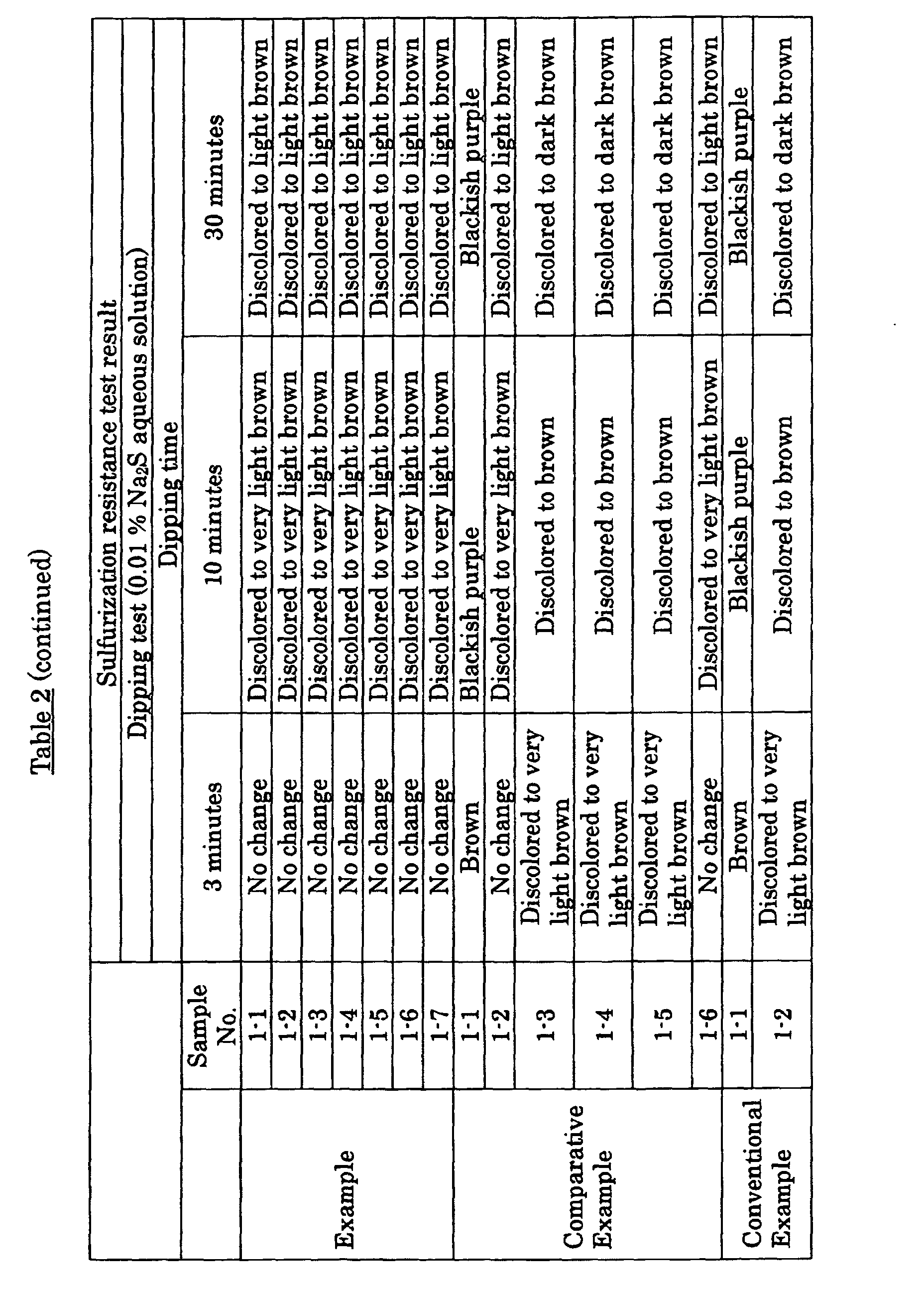
- the glass substrate thus obtained on which the thin film was adhered was exposed in the air to test an acid resistance. Further, different glass substrates on which the thin film was adhered each were dipped in a 10 % sodium chloride (NaCl) aqueous solution and a 0.01 sodium sulfide (Na 2 S) aqueous solution to test a halogen (chlorine) resistance and a sulfurization resistance. In the respective tests, the state of the thin films after prescribed time was passed was visually evaluated. The results thereof are shown in the following Table 2.
- Comparative Example 1-5 it can be found that when a transition metal such as Ti is substituted for the metal component (A) of the present invention, the resulting Ag alloy is not improved in a sulfurization resistance.
- the Ag alloy of the present invention is improved in a corrosion resistance while having a high reflectance.
- a dye compound containing a halogen element (Cl, Br, I and the like) is applied as a recording layer on a disc-like substrate as described in Japanese Patent Application Laid-Open No. 321110/1999 and Japanese Patent Application Laid-Open No. 43420/2000, and a reflective layer and a protective layer are further provided thereon.
- halogen ions contained in these dye compounds are adhered onto Ag, Ag is discolored.
- the dye is decomposed and the halogen ions contained in the dye are adhered onto the Ag reflective layer, it is reacted with the halogen ions and discolored to reduce a reflectance.
- Example 2-1 Ag-1 mass%In-0.7 mass%Pd 2-2 Ag-1 mass%Sn-0.8 mass%Au 2-3 Ag-0.8 mass%Zn-0.8 mass%Au Comparative Example 2-1 Ag-0.01 mass%Zn-0.01 mass%Au-0.1 mass%Cu 2-2 Ag-1 mass%Au 2-3 Ag-1 mass%Sn 2-4 Ag-1 mass%Ti-1 mass%Au 2-5 Ag-1 mass%Mg-1 mass%Au Conventional Example 2-1 Ag 2-2 Ag-0.9 mass%Pd-1 mass%Cu 2-3 Ag-1 mass%Mg Test solution 10 % Sodium chlorate aqueous solution 10 % Potassium iodide aqueous solution Dipping time 380 hours 24 hours Sample No. Sample No. Sample No.
- the Ag alloy when used for those related to liquid crystal and reflecting films in DVD, DVD-RW and DVD-RAM, they are exposed to a high temperature in a certain case depending on the use conditions thereof. For example, when a thin film of pure silver is exposed to a temperature of 200°C or higher, the film causes coagulation to become turbid and white, and it is reduced in a reflectance in a certain case. Accordingly, a stability of the film against heat is required in these uses.
- Example 3-1 Ag-1.0 mass%In-0.7 mass%Pd 3-2 Ag-0.8 mass%Sn-0.6 mass%Au-0.2 mass%Pd 3-3 Ag-1.0 mass%Zn-0.8 mass%Au 3-4 Ag-0.2 mass%Zn-0.5 mass%Au 3-5 Ag-0.2 mass%Zn-0.6 mass%Pd 3-6 Ag-0.3 mass%In-0.7 mass%Pd Comparative Example 3-1 Ag-0.5 mass%Au 3-2 Ag-0.2 mass%Zn-0.6 mass%Au-4.0 mass%Cu Conventional Example 3-1 Ag 3-2 Ag-0.9 mass%Pd-1 mass%Cu
- Example 3-1 100 94 100 3-2 100 97 100 3-3 100 97 99 3-4 100 97 100 3-5 100 98 100 3-6 100 97 100 Comparative Example 3-1 100 92 100 3-2 100 87 98 Conventional Example 3-1 100 84 99 3-2 100 90 100
- Example 3-4 has a change rate of 98 % and is thermally very stable but the thin film containing no Zn prepared in Comparative Example 3-1 has a change rate of 92 % and is improved in a thermal stability by adding Au and Zn in combination according to the present invention.
Landscapes
- Chemical & Material Sciences (AREA)
- Engineering & Computer Science (AREA)
- Organic Chemistry (AREA)
- Materials Engineering (AREA)
- Mechanical Engineering (AREA)
- Metallurgy (AREA)
- Chemical Kinetics & Catalysis (AREA)
- Manufacturing & Machinery (AREA)
- Physical Vapour Deposition (AREA)
- Optical Record Carriers And Manufacture Thereof (AREA)
- Manufacturing Optical Record Carriers (AREA)
- Liquid Crystal (AREA)
- Electroluminescent Light Sources (AREA)
Abstract
Description
| Sample No. | Composition | |
| Example | 1-1 | Ag-1 mass%In-0.7 mass%Pd |
| 1-2 | Ag-1 mass%Zn-0.5 mass%Au | |
| 1-3 | Ag-0.8 mass%Sn-0.6 mass%Au-0.2 mass%Pd | |
| 1-4 | Ag-0.5 mass%In-0.6 mass%Au-0.2 mass%Pt | |
| 1-5 | Ag-0.8 mass%In-0.5 mass%Au-0.5 mass%Cu | |
| 1-6 | Ag-0.7 mass%Sn-0.7 mass%Pt | |
| 1-7 | Ag-0.3 mass%In-0.7 mass%Pd | |
| Comparative Example | 1-1 | Ag-0.01 mass%Zn-0.01 mass%Au-0.1 mass%Cu |
| 1-2 | Ag-2 mass%In-4 mass%Pd | |
| 1-3 | Ag-1 mass%Au | |
| 1-4 | Ag-1 mass%Pd | |
| 1-5 | Ag-1 mass%Au-1 mass%Ti | |
| 1-6 | Ag-1 mass%Sn | |
| Conventional Example | 1-1 | Ag |
| 1-2 | Ag-0.9 mass%Pd-1 mass%Cu |

| Sample No. | Electrical resistivity ρ/µΩ·cm | |
| Example | 1-1 | 2.5 |
| 1-2 | 2.0 | |
| 1-3 | 4.8 | |
| 1-4 | 3.2 | |
| 1-5 | 2.9 | |
| 1-6 | 6.4 | |
| 1-7 | 2.3 | |
| Comparative Example | 1-2 | 7.9 |
| Sample No. | Composition | |
| Example | 2-1 | Ag-1 mass%In-0.7 mass%Pd |
| 2-2 | Ag-1 mass%Sn-0.8 mass%Au | |
| 2-3 | Ag-0.8 mass%Zn-0.8 mass%Au | |
| Comparative Example | 2-1 | Ag-0.01 mass%Zn-0.01 mass%Au-0.1 mass%Cu |
| 2-2 | Ag-1 mass%Au | |
| 2-3 | Ag-1 mass%Sn | |
| 2-4 | Ag-1 mass%Ti-1 mass%Au | |
| 2-5 | Ag-1 mass%Mg-1 mass%Au | |
| Conventional Example | 2-1 | Ag |
| 2-2 | Ag-0.9 mass%Pd-1 mass%Cu | |
| 2-3 | Ag-1 mass%Mg |
| Test solution | 10 % Sodium chlorate aqueous solution | 10 % Potassium iodide aqueous solution | |
| Dipping time | 380 hours | 24 hours | |
| Sample No. Sample No. | Color difference b (= +yellow/-blue) | Color difference b (= +yellow/-blue) | |
| Example | 2-1 | 0.45 | 0.03 |
| 2-2 | 0.80 | 0.52 | |
| 2-3 | 0.41 | 0.65 | |
| Comparative Example | 2-1 | 4.80 | 8.53 |
| 2-2 | 1.65 | 1.31 | |
| 2-3 | 2.89 | 4.19 | |
| 2-4 | 1.85 | 1.56 | |
| 2-5 | 2.03 | 1.87 | |
| Conventional Example | 2-1 | 4.78 | 8.80 |
| 2-2 | 2.19 | 2.44 | |
| 2-3 | 3.65 | 5.00 |
| Sample No. | Composition | |
| Example | 3-1 | Ag-1.0 mass%In-0.7 mass%Pd |
| 3-2 | Ag-0.8 mass%Sn-0.6 mass%Au-0.2 mass%Pd | |
| 3-3 | Ag-1.0 mass%Zn-0.8 mass%Au | |
| 3-4 | Ag-0.2 mass%Zn-0.5 mass%Au | |
| 3-5 | Ag-0.2 mass%Zn-0.6 mass%Pd | |
| 3-6 | Ag-0.3 mass%In-0.7 mass%Pd | |
| Comparative Example | 3-1 | Ag-0.5 mass%Au |
| 3-2 | Ag-0.2 mass%Zn-0.6 mass%Au-4.0 mass%Cu | |
| Conventional Example | 3-1 | Ag |
| 3-2 | Ag-0.9 mass%Pd-1 mass%Cu |
| Sample No. No | Change rate (%) | |||
| Before test | After test | |||
| . | Measuring wavelength 400 nm | Measuring wavelength 700 mn | ||
| Example | 3-1 | 100 | 94 | 100 |
| 3-2 | 100 | 97 | 100 | |
| 3-3 | 100 | 97 | 99 | |
| 3-4 | 100 | 97 | 100 | |
| 3-5 | 100 | 98 | 100 | |
| 3-6 | 100 | 97 | 100 | |
| Comparative Example | 3-1 | 100 | 92 | 100 |
| 3-2 | 100 | 87 | 98 | |
| Conventional Example | 3-1 | 100 | 84 | 99 |
| 3-2 | 100 | 90 | 100 |
| Sample No. | Composition | |
| Example | 4-1 | Ag-0.8 mass%In-0.3 mass%Pt |
| 4-2 | Ag-1.0 mass%Zn-0.5 mass%Au | |
| 4-3 | Ag-1.0 mass%Zn-2.0 mass%Pd | |
| Comparative Example | 4-1 | Ag-0.8 mass%Sn-2.0 mass%Au |
| 4-2 | Ag-0.8 mass%Sn-2.0 mass %Pt |
| Sample No. | Evaluation | Remarks | |
| Example | 4-1 | ○ | Good |
| 4-2 | ○ | Good | |
| 4-3 | ○ | Good | |
| Comparative Example | 4-1 | × | Residue present |
| 4-2 | × | Residue present | |
| Evaluation criteria O: no residue is adhered on the substrate ×: residue is adhered on the substrate |
Claims (20)
- A sputtering target material for forming a high corrosion resistant thin film having a high reflectance, comprising an Ag alloy which is prepared by blending Ag with at least one metal component (A) selected from 0.1 to 2.0 mass % of In, 0.1 to 2.0 mass % of Sn and 0.1 to 2.0 mass % of Zn in an amount of 0.1 to 2.0 mass % in total and at least one metal component (B) selected from 0.1 to 0.9 mass % of Au, 0.1 to 4.9 mass % of Pd and 0.1 to 0.9 mass % of Pt in an amount of 0.1 to 4.9 mass % in total and in which the total content of the metal component (A) and the metal component (B) is 0.2 to 5.0 mass %.
- A sputtering target material for forming a high corrosion resistant thin film having a high reflectance, comprising an Ag alloy which is prepared by blending Ag with a at least one metal component (A) selected from 0.05 to 2.0 mass % of In, 0.05 to 2.0 mass % of Sn and 0.05 to 2.0 mass % of Zn in an amount of 0.05 to 2.0 mass % in total, at least metal component (B) selected from 0.1 to 0.9 mass % of Au, 0.1 to 4.9 mass % of Pd and 0.1 to 0.9 mass % of Pt in an amount of 0.1 to 4.9 mass % in total and 0.05 to 2.0 mass % of Cu and in which the total content of the metal component (A), the metal component (B) and Cu is 0.2 to 5.0 mass %.
- The sputtering target material as described in claim 1 or 2, wherein the metal component (A) is at least one selected from 0.1 to 1.5 mass % of In, 0.1 to 1.0 mass % of Sn and 0.1 to 1.5 mass % of Zn.
- The sputtering target material as described in claim 1 or 2, wherein the total content of the metal component (A) is 0.1 to 1.5 mass %.
- The sputtering target material as described in claim 1 or 2, wherein the metal component (B) is at least one selected from 0.2 to 0.8 mass % of Au, 0.2 to 2.0 mass % of Pd and 0.2 to 0.8 mass % of Pt.
- The sputtering target material as described in claim 1 or 2, wherein the total content of the metal component (B) is 0.2 to 0.9 mass %.
- The sputtering target material as described in claim 1, wherein the total content of the metal component (A) and the metal component (B) is 0.3 to 2.0 mass %.
- The sputtering target material as described in claim 2, wherein Cu has a content of 0.1 to 1.5 mass %.
- The sputtering target material as described in claim 2, wherein the total content of the metal component (A), the metal component (B) and Cu is 0.5 to 2.0 mass %.
- A thin film of an Ag alloy which is prepared by blending Ag with at least one metal component (A) selected from 0.1 to 2.0 mass % of In, 0.1 to 2.0 mass % of Sn and 0.1 to 2.0 mass % of Zn in an amount of 0.1 to 2.0 mass % in total and at least one metal component (B) selected from 0.1 to 0.9 mass % of Au, 0.1 to 4.9 mass % of Pd and 0.1 to 0.9 mass % of Pt in an amount of 0.1 to 4.9 mass % in total and in which the total content of the metal component (A) and the metal component (B) is 0.2 to 5.0 mass %.
- A thin film of an Ag alloy which is prepared by blending Ag with at least one metal component (A) selected from 0.05 to 2.0 mass % of In, 0.05 to 2.0 mass % of Sn and 0.05 to 2.0 mass % of Zn in an amount of 0.05 to 2.0 mass % in total, at least one metal component (B) selected from 0.1 to 0.9 mass % of Au, 0.1 to 4.9 mass % of Pd and 0.1 to 0.9 mass % of Pt in an amount of 0.1 to 4.9 mass % in total and 0.05 to 2.0 mass % of Cu and in which the total content of the metal component (A), the metal component (B) and Cu is 0.2 to 5.0 mass %.
- The thin film as described in claim 10 or 11, wherein the metal component (A) is at least one selected from 0.1 to 1.5 mass % of In, 0.1 to 1.0 mass % of Sn and 0.1 to 1.5 mass % of Zn.
- The thin film as described in claim 10 or 11, wherein the total content of the metal component (A) is 0.1 to 1.5 mass %.
- The thin film as described in claim 10 or 11, wherein the metal component (B) is at least one selected from 0.2 to 0.8 mass % of Au, 0.2 to 2.0 mass % of Pd and 0.2 to 0.8 mass % of Pt.
- The thin film as described in claim 10 or 11, wherein the total content of the metal component (B) is 0.2 to 0.9 mass %.
- The thin film as described in claim 10, wherein the total content of the metal component (A) and the metal component (B) is 0.3 to 2.0 mass %.
- The thin film as described in claim 11, wherein Cu has a content of 0.1 to 1.5 mass %.
- The thin film as described in claim 11, wherein the total content of the metal component (A), the metal component (B) and Cu is 0.5 to 2.0 mass %.
- An optical disc medium comprising the thin film as described in claim 10 or 11.
- A reflection type STN liquid crystal display and an organic EL display prepared by using the thin film as described in claim 10 or 11.
Applications Claiming Priority (3)
| Application Number | Priority Date | Filing Date | Title |
|---|---|---|---|
| JP2001076132 | 2001-03-16 | ||
| JP2001076132 | 2001-03-16 | ||
| PCT/JP2002/002466 WO2002077317A1 (en) | 2001-03-16 | 2002-03-15 | Sputtering target material |
Publications (3)
| Publication Number | Publication Date |
|---|---|
| EP1371749A1 true EP1371749A1 (en) | 2003-12-17 |
| EP1371749A4 EP1371749A4 (en) | 2004-08-18 |
| EP1371749B1 EP1371749B1 (en) | 2009-01-07 |
Family
ID=18933115
Family Applications (1)
| Application Number | Title | Priority Date | Filing Date |
|---|---|---|---|
| EP02705228A Expired - Lifetime EP1371749B1 (en) | 2001-03-16 | 2002-03-15 | Optical disc medium, reflection type STN liquid crystal display and organic EL display |
Country Status (8)
| Country | Link |
|---|---|
| US (1) | US7465424B2 (en) |
| EP (1) | EP1371749B1 (en) |
| JP (1) | JP3856386B2 (en) |
| CN (1) | CN1217028C (en) |
| AT (1) | ATE420219T1 (en) |
| DE (1) | DE60230728D1 (en) |
| TW (1) | TW575674B (en) |
| WO (1) | WO2002077317A1 (en) |
Cited By (5)
| Publication number | Priority date | Publication date | Assignee | Title |
|---|---|---|---|---|
| EP1617427A3 (en) * | 2004-07-15 | 2006-03-15 | Kabushiki Kaisha Kobe Seiko Sho | Silver alloy reflective film, sputtering target therefor, and optical information recording medium using the same |
| EP1660316A4 (en) * | 2003-09-03 | 2008-08-20 | Williams Advanced Materials In | Silver alloys for optical data storages and optical media containing same |
| EP1736558A4 (en) * | 2003-12-10 | 2009-06-17 | Tanaka Precious Metal Ind | SILVER ALLOY FOR REFLECTIVE FILM |
| ITSA20120001A1 (en) * | 2012-01-04 | 2013-07-05 | Rosita Gioielli D Amare Di Petrosin O Rosa | SILVER-PALLADIUM LEAGUE FOR THE SILVER SILVER INDUSTRY. |
| EP2937444A4 (en) * | 2012-12-21 | 2016-08-17 | Mitsubishi Materials Corp | ALLOY SPRAY TARGET Ag-In |
Families Citing this family (21)
| Publication number | Priority date | Publication date | Assignee | Title |
|---|---|---|---|---|
| JP2004192702A (en) * | 2002-12-10 | 2004-07-08 | Tanaka Kikinzoku Kogyo Kk | Silver alloy for reflection film of optical recording medium |
| JP4671579B2 (en) | 2002-12-16 | 2011-04-20 | 株式会社アルバック | Ag alloy reflective film and method for producing the same |
| KR100677805B1 (en) * | 2003-07-23 | 2007-02-02 | 샤프 가부시키가이샤 | Silver alloy materials, circuit boards, electronic devices and methods of manufacturing circuit boards |
| CN101042946B (en) * | 2003-07-23 | 2011-04-20 | 夏普株式会社 | Silver alloy material, circuit board, electronic device and method of producing circuit board |
| EP1669964A4 (en) * | 2003-09-30 | 2007-09-26 | Asahi Glass Co Ltd | MULTILAYER BODIES FOR FORMING A WIRING BASE, WIRING BASE, AND PROCESS FOR PRODUCING THE SAME |
| EP1734140A4 (en) * | 2003-12-10 | 2009-06-24 | Tanaka Precious Metal Ind | SILVER ALLOY HAVING EXCELLENT PRESERVATION OF REFLECTION FACTOR |
| JP4918231B2 (en) * | 2004-06-16 | 2012-04-18 | 株式会社アルバック | Method for producing Ag alloy film |
| WO2006132417A1 (en) * | 2005-06-10 | 2006-12-14 | Tanaka Kikinzoku Kogyo K.K. | Silver alloy excellent in reflectance/transmittance maintaining characteristics |
| WO2006132413A1 (en) * | 2005-06-10 | 2006-12-14 | Tanaka Kikinzoku Kogyo K.K. | Silver alloy for electrode, wiring and electromagnetic shielding |
| JP4833942B2 (en) * | 2007-08-29 | 2011-12-07 | 株式会社コベルコ科研 | Ag-based alloy sputtering target |
| JP2010287565A (en) * | 2009-05-14 | 2010-12-24 | Mitsubishi Materials Corp | Al alloy reflective electrode film forming anode layer of upper light emitting organic EL device |
| JP4793502B2 (en) | 2009-10-06 | 2011-10-12 | 三菱マテリアル株式会社 | Silver alloy target for forming reflective electrode film of organic EL element and method for producing the same |
| JP5533545B2 (en) * | 2010-01-12 | 2014-06-25 | 三菱マテリアル株式会社 | Silver alloy target for forming reflective electrode film of organic EL element and method for producing the same |
| JP5159962B1 (en) | 2012-01-10 | 2013-03-13 | 三菱マテリアル株式会社 | Silver alloy sputtering target for forming conductive film and method for producing the same |
| JP5612147B2 (en) * | 2013-03-11 | 2014-10-22 | 三菱マテリアル株式会社 | Silver alloy sputtering target for forming conductive film and method for producing the same |
| JP6198177B2 (en) * | 2013-07-19 | 2017-09-20 | 三菱マテリアル株式会社 | Ag alloy sputtering target |
| CN105316630B (en) * | 2014-06-04 | 2020-06-19 | 光洋应用材料科技股份有限公司 | Silver alloy target, its manufacturing method and organic light-emitting diode using the same |
| TWI612025B (en) * | 2015-09-23 | 2018-01-21 | 住華科技股份有限公司 | Solder for fabricating sputtering target and applying method thereof |
| CN106947879B (en) * | 2017-04-11 | 2019-02-19 | 东北大学 | Silver-based alloy target blank for vacuum magnetron sputtering, preparation method and application thereof |
| JP2020090706A (en) * | 2018-12-05 | 2020-06-11 | 三菱マテリアル株式会社 | Metal film and sputtering target |
| CN113564543A (en) * | 2021-07-20 | 2021-10-29 | 昆山嘉美荣材料科技有限公司 | Silver palladium indium target material and preparation method thereof |
Family Cites Families (15)
| Publication number | Priority date | Publication date | Assignee | Title |
|---|---|---|---|---|
| JP2541677B2 (en) | 1989-08-09 | 1996-10-09 | 帝人株式会社 | Optical recording medium |
| CA2017284C (en) | 1989-07-04 | 1995-10-03 | Kazutomi Suzuki | Optical recording medium |
| JPH073435A (en) | 1993-04-22 | 1995-01-06 | Mitsubishi Materials Corp | High corrosion resistance Ag-Mg alloy and thin film thereof |
| JP3558301B2 (en) | 1993-04-22 | 2004-08-25 | 三菱マテリアル株式会社 | High corrosion resistant Ag-Mg alloy thin film |
| JPH09111380A (en) * | 1995-10-18 | 1997-04-28 | Nisshin Steel Co Ltd | Ag-cu-zn alloy excellent in antibacterial and antimold property |
| JPH10177742A (en) | 1996-10-15 | 1998-06-30 | Kao Corp | Optical recording medium |
| JPH10143917A (en) * | 1996-11-08 | 1998-05-29 | Kao Corp | Optical recording medium |
| CN1080767C (en) * | 1997-07-02 | 2002-03-13 | 马渊马达株式会社 | Sliding contact material, clad composite material, and small D. C. motor made by using the same |
| JPH1125515A (en) * | 1997-07-03 | 1999-01-29 | Kao Corp | Optical recording medium |
| US6544616B2 (en) * | 2000-07-21 | 2003-04-08 | Target Technology Company, Llc | Metal alloys for the reflective or the semi-reflective layer of an optical storage medium |
| JP4007702B2 (en) | 1998-10-05 | 2007-11-14 | 株式会社フルヤ金属 | Sputtering target material for forming a thin film, a thin film formed using the same, and an optical recording medium |
| JP2000226626A (en) * | 1999-02-03 | 2000-08-15 | Tsutomu Kirihara | Sulfidization resistant silver alloy |
| JP4247863B2 (en) | 1999-07-12 | 2009-04-02 | ソニー株式会社 | Metal materials for electronic components, wiring materials for electronic components, electrode materials for electronic components, electronic components, electronic equipment, processing methods for metal materials, and electro-optical components |
| JP3957259B2 (en) | 2000-04-12 | 2007-08-15 | 株式会社神戸製鋼所 | Reflective layer for optical information recording medium and optical information recording medium |
| JP2002235130A (en) | 2001-02-05 | 2002-08-23 | Sumitomo Metal Mining Co Ltd | Silver alloy for optical disk reflective film |
-
2002
- 2002-03-15 JP JP2002575350A patent/JP3856386B2/en not_active Expired - Fee Related
- 2002-03-15 DE DE60230728T patent/DE60230728D1/en not_active Expired - Lifetime
- 2002-03-15 WO PCT/JP2002/002466 patent/WO2002077317A1/en not_active Ceased
- 2002-03-15 CN CN028007182A patent/CN1217028C/en not_active Expired - Fee Related
- 2002-03-15 EP EP02705228A patent/EP1371749B1/en not_active Expired - Lifetime
- 2002-03-15 AT AT02705228T patent/ATE420219T1/en not_active IP Right Cessation
- 2002-03-15 US US10/470,414 patent/US7465424B2/en not_active Expired - Fee Related
- 2002-03-15 TW TW91104906A patent/TW575674B/en not_active IP Right Cessation
Cited By (8)
| Publication number | Priority date | Publication date | Assignee | Title |
|---|---|---|---|---|
| EP1660316A4 (en) * | 2003-09-03 | 2008-08-20 | Williams Advanced Materials In | Silver alloys for optical data storages and optical media containing same |
| EP1736558A4 (en) * | 2003-12-10 | 2009-06-17 | Tanaka Precious Metal Ind | SILVER ALLOY FOR REFLECTIVE FILM |
| EP1617427A3 (en) * | 2004-07-15 | 2006-03-15 | Kabushiki Kaisha Kobe Seiko Sho | Silver alloy reflective film, sputtering target therefor, and optical information recording medium using the same |
| EP2043097A1 (en) * | 2004-07-15 | 2009-04-01 | Kabushiki Kaisha Kobe Seiko Sho | Silver alloy reflective film, and optical information recording medium using the same |
| EP2077556A1 (en) * | 2004-07-15 | 2009-07-08 | Kabushiki Kaisha Kobe Seiko Sho | Silver alloy reflective film, sputtering target therefor, and optical information recording medium using the same |
| US7695790B2 (en) | 2004-07-15 | 2010-04-13 | Kobe Steel, Ltd. | Silver alloy reflective film, sputtering target therefor, and optical information recording medium using the same |
| ITSA20120001A1 (en) * | 2012-01-04 | 2013-07-05 | Rosita Gioielli D Amare Di Petrosin O Rosa | SILVER-PALLADIUM LEAGUE FOR THE SILVER SILVER INDUSTRY. |
| EP2937444A4 (en) * | 2012-12-21 | 2016-08-17 | Mitsubishi Materials Corp | ALLOY SPRAY TARGET Ag-In |
Also Published As
| Publication number | Publication date |
|---|---|
| US7465424B2 (en) | 2008-12-16 |
| CN1458986A (en) | 2003-11-26 |
| US20040055882A1 (en) | 2004-03-25 |
| JPWO2002077317A1 (en) | 2004-07-15 |
| JP3856386B2 (en) | 2006-12-13 |
| EP1371749B1 (en) | 2009-01-07 |
| ATE420219T1 (en) | 2009-01-15 |
| DE60230728D1 (en) | 2009-02-26 |
| WO2002077317A1 (en) | 2002-10-03 |
| TW575674B (en) | 2004-02-11 |
| EP1371749A4 (en) | 2004-08-18 |
| CN1217028C (en) | 2005-08-31 |
Similar Documents
| Publication | Publication Date | Title |
|---|---|---|
| US7465424B2 (en) | Sputtering target material | |
| US8252127B2 (en) | Sputtering target material | |
| JP4801279B2 (en) | Sputtering target material | |
| JP2005048231A (en) | Sputtering target material | |
| JP3855958B2 (en) | Sputtering target material | |
| KR100841588B1 (en) | Sputtering target material | |
| JP4418777B2 (en) | Sputtering target material and thin film made of Ag-based alloy | |
| TWI283710B (en) | Spattering targets material | |
| JP5590258B2 (en) | Ag alloy film forming sputtering target, Ag alloy film, Ag alloy reflective film, Ag alloy conductive film, Ag alloy semi-transmissive film | |
| JP3765540B2 (en) | Silver alloy for reflective film of optical recording media | |
| JP2003160859A (en) | Silver alloy sputtering target for forming reflective film on optical recording media | |
| JP4186221B2 (en) | Reflective film and translucent reflective film for optical recording medium, and Ag alloy sputtering target for forming these reflective films | |
| JP2003160860A (en) | Silver alloy sputtering target for forming reflective film on optical recording media | |
| JP4585952B2 (en) | Thin film made of Ag-based alloy | |
| JP2003193155A (en) | Silver alloy sputtering target for forming reflection film of optical recording medium and reflection film formed using this target | |
| JP4186222B2 (en) | Reflective film and translucent reflective film for optical recording medium, and Ag alloy sputtering target for forming these reflective films | |
| JP2007310967A (en) | Translucent reflective film for optical recording medium and Ag alloy sputtering target for forming the translucent reflective film | |
| JPH04280960A (en) | Thin al alloy film and al alloy sputtering target | |
| JP2006099821A (en) | Reflective film and translucent reflective film for optical recording medium, and Ag alloy sputtering target for forming these reflective films | |
| JP2007003624A (en) | Semi-reflective semi-permeable membrane | |
| CN101346491A (en) | Semitransparent reflective film and reflective film for optical recording medium, and Ag alloy sputtering target for forming semitransparent reflective film and reflective film | |
| JP2007026501A (en) | Translucent reflective film for optical recording medium and Ag alloy sputtering target for forming the translucent reflective film |
Legal Events
| Date | Code | Title | Description |
|---|---|---|---|
| PUAI | Public reference made under article 153(3) epc to a published international application that has entered the european phase |
Free format text: ORIGINAL CODE: 0009012 |
|
| 17P | Request for examination filed |
Effective date: 20030725 |
|
| AK | Designated contracting states |
Kind code of ref document: A1 Designated state(s): AT BE CH CY DE DK ES FI FR GB GR IE IT LI LU MC NL PT SE TR |
|
| A4 | Supplementary search report drawn up and despatched |
Effective date: 20040706 |
|
| RAP1 | Party data changed (applicant data changed or rights of an application transferred) |
Owner name: ISHIFUKU METAL INDUSTRY CO., LTD. |
|
| GRAP | Despatch of communication of intention to grant a patent |
Free format text: ORIGINAL CODE: EPIDOSNIGR1 |
|
| RTI1 | Title (correction) |
Free format text: OPTICAL DISC MEDIUM, REFLECTION TYPE STN LIQUID CRYSTAL DISPLAY AND ORGANIC EL DISPLAY |
|
| GRAS | Grant fee paid |
Free format text: ORIGINAL CODE: EPIDOSNIGR3 |
|
| GRAA | (expected) grant |
Free format text: ORIGINAL CODE: 0009210 |
|
| RIN1 | Information on inventor provided before grant (corrected) |
Inventor name: HASEGAWA, KOICHI,C/O ISHIFUKU METAL IND. CO., LTD. Inventor name: ISHII, NOBUO,C/O ISHIFUKU METAL IND. CO., LTD. Inventor name: ASAKI, TOMOYOSHI,C/O ISHIFUKU METAL IND. CO., LTD. |
|
| AK | Designated contracting states |
Kind code of ref document: B1 Designated state(s): AT BE CH CY DE DK ES FI FR GB GR IE IT LI LU MC NL PT SE TR |
|
| REG | Reference to a national code |
Ref country code: GB Ref legal event code: FG4D |
|
| REG | Reference to a national code |
Ref country code: CH Ref legal event code: EP |
|
| REG | Reference to a national code |
Ref country code: IE Ref legal event code: FG4D |
|
| REF | Corresponds to: |
Ref document number: 60230728 Country of ref document: DE Date of ref document: 20090226 Kind code of ref document: P |
|
| PG25 | Lapsed in a contracting state [announced via postgrant information from national office to epo] |
Ref country code: ES Free format text: LAPSE BECAUSE OF FAILURE TO SUBMIT A TRANSLATION OF THE DESCRIPTION OR TO PAY THE FEE WITHIN THE PRESCRIBED TIME-LIMIT Effective date: 20090418 Ref country code: FI Free format text: LAPSE BECAUSE OF FAILURE TO SUBMIT A TRANSLATION OF THE DESCRIPTION OR TO PAY THE FEE WITHIN THE PRESCRIBED TIME-LIMIT Effective date: 20090107 |
|
| PG25 | Lapsed in a contracting state [announced via postgrant information from national office to epo] |
Ref country code: SE Free format text: LAPSE BECAUSE OF FAILURE TO SUBMIT A TRANSLATION OF THE DESCRIPTION OR TO PAY THE FEE WITHIN THE PRESCRIBED TIME-LIMIT Effective date: 20090407 Ref country code: PT Free format text: LAPSE BECAUSE OF FAILURE TO SUBMIT A TRANSLATION OF THE DESCRIPTION OR TO PAY THE FEE WITHIN THE PRESCRIBED TIME-LIMIT Effective date: 20090608 Ref country code: AT Free format text: LAPSE BECAUSE OF FAILURE TO SUBMIT A TRANSLATION OF THE DESCRIPTION OR TO PAY THE FEE WITHIN THE PRESCRIBED TIME-LIMIT Effective date: 20090107 |
|
| PG25 | Lapsed in a contracting state [announced via postgrant information from national office to epo] |
Ref country code: BE Free format text: LAPSE BECAUSE OF FAILURE TO SUBMIT A TRANSLATION OF THE DESCRIPTION OR TO PAY THE FEE WITHIN THE PRESCRIBED TIME-LIMIT Effective date: 20090107 |
|
| PG25 | Lapsed in a contracting state [announced via postgrant information from national office to epo] |
Ref country code: MC Free format text: LAPSE BECAUSE OF NON-PAYMENT OF DUE FEES Effective date: 20090331 Ref country code: DK Free format text: LAPSE BECAUSE OF FAILURE TO SUBMIT A TRANSLATION OF THE DESCRIPTION OR TO PAY THE FEE WITHIN THE PRESCRIBED TIME-LIMIT Effective date: 20090107 |
|
| REG | Reference to a national code |
Ref country code: CH Ref legal event code: PL |
|
| PLBE | No opposition filed within time limit |
Free format text: ORIGINAL CODE: 0009261 |
|
| STAA | Information on the status of an ep patent application or granted ep patent |
Free format text: STATUS: NO OPPOSITION FILED WITHIN TIME LIMIT |
|
| 26N | No opposition filed |
Effective date: 20091008 |
|
| GBPC | Gb: european patent ceased through non-payment of renewal fee |
Effective date: 20090407 |
|
| REG | Reference to a national code |
Ref country code: FR Ref legal event code: ST Effective date: 20091130 |
|
| PG25 | Lapsed in a contracting state [announced via postgrant information from national office to epo] |
Ref country code: CH Free format text: LAPSE BECAUSE OF NON-PAYMENT OF DUE FEES Effective date: 20090331 Ref country code: LI Free format text: LAPSE BECAUSE OF NON-PAYMENT OF DUE FEES Effective date: 20090331 Ref country code: IE Free format text: LAPSE BECAUSE OF NON-PAYMENT OF DUE FEES Effective date: 20090315 |
|
| PG25 | Lapsed in a contracting state [announced via postgrant information from national office to epo] |
Ref country code: GB Free format text: LAPSE BECAUSE OF NON-PAYMENT OF DUE FEES Effective date: 20090407 Ref country code: FR Free format text: LAPSE BECAUSE OF NON-PAYMENT OF DUE FEES Effective date: 20091123 |
|
| PG25 | Lapsed in a contracting state [announced via postgrant information from national office to epo] |
Ref country code: GR Free format text: LAPSE BECAUSE OF FAILURE TO SUBMIT A TRANSLATION OF THE DESCRIPTION OR TO PAY THE FEE WITHIN THE PRESCRIBED TIME-LIMIT Effective date: 20090408 |
|
| PG25 | Lapsed in a contracting state [announced via postgrant information from national office to epo] |
Ref country code: IT Free format text: LAPSE BECAUSE OF FAILURE TO SUBMIT A TRANSLATION OF THE DESCRIPTION OR TO PAY THE FEE WITHIN THE PRESCRIBED TIME-LIMIT Effective date: 20090107 |
|
| PG25 | Lapsed in a contracting state [announced via postgrant information from national office to epo] |
Ref country code: LU Free format text: LAPSE BECAUSE OF NON-PAYMENT OF DUE FEES Effective date: 20090315 |
|
| PG25 | Lapsed in a contracting state [announced via postgrant information from national office to epo] |
Ref country code: TR Free format text: LAPSE BECAUSE OF FAILURE TO SUBMIT A TRANSLATION OF THE DESCRIPTION OR TO PAY THE FEE WITHIN THE PRESCRIBED TIME-LIMIT Effective date: 20090107 |
|
| PG25 | Lapsed in a contracting state [announced via postgrant information from national office to epo] |
Ref country code: CY Free format text: LAPSE BECAUSE OF FAILURE TO SUBMIT A TRANSLATION OF THE DESCRIPTION OR TO PAY THE FEE WITHIN THE PRESCRIBED TIME-LIMIT Effective date: 20090107 |
|
| PGFP | Annual fee paid to national office [announced via postgrant information from national office to epo] |
Ref country code: NL Payment date: 20150130 Year of fee payment: 14 |
|
| PGFP | Annual fee paid to national office [announced via postgrant information from national office to epo] |
Ref country code: DE Payment date: 20150306 Year of fee payment: 14 |
|
| REG | Reference to a national code |
Ref country code: DE Ref legal event code: R119 Ref document number: 60230728 Country of ref document: DE |
|
| REG | Reference to a national code |
Ref country code: NL Ref legal event code: MM Effective date: 20160401 |
|
| PG25 | Lapsed in a contracting state [announced via postgrant information from national office to epo] |
Ref country code: DE Free format text: LAPSE BECAUSE OF NON-PAYMENT OF DUE FEES Effective date: 20161001 Ref country code: NL Free format text: LAPSE BECAUSE OF NON-PAYMENT OF DUE FEES Effective date: 20160401 |