EP2043097A1 - Silver alloy reflective film, and optical information recording medium using the same - Google Patents
Silver alloy reflective film, and optical information recording medium using the same Download PDFInfo
- Publication number
- EP2043097A1 EP2043097A1 EP08020402A EP08020402A EP2043097A1 EP 2043097 A1 EP2043097 A1 EP 2043097A1 EP 08020402 A EP08020402 A EP 08020402A EP 08020402 A EP08020402 A EP 08020402A EP 2043097 A1 EP2043097 A1 EP 2043097A1
- Authority
- EP
- European Patent Office
- Prior art keywords
- alloy
- atomic percent
- reflective film
- information recording
- recording medium
- Prior art date
- Legal status (The legal status is an assumption and is not a legal conclusion. Google has not performed a legal analysis and makes no representation as to the accuracy of the status listed.)
- Withdrawn
Links
Images
Classifications
-
- C—CHEMISTRY; METALLURGY
- C23—COATING METALLIC MATERIAL; COATING MATERIAL WITH METALLIC MATERIAL; CHEMICAL SURFACE TREATMENT; DIFFUSION TREATMENT OF METALLIC MATERIAL; COATING BY VACUUM EVAPORATION, BY SPUTTERING, BY ION IMPLANTATION OR BY CHEMICAL VAPOUR DEPOSITION, IN GENERAL; INHIBITING CORROSION OF METALLIC MATERIAL OR INCRUSTATION IN GENERAL
- C23C—COATING METALLIC MATERIAL; COATING MATERIAL WITH METALLIC MATERIAL; SURFACE TREATMENT OF METALLIC MATERIAL BY DIFFUSION INTO THE SURFACE, BY CHEMICAL CONVERSION OR SUBSTITUTION; COATING BY VACUUM EVAPORATION, BY SPUTTERING, BY ION IMPLANTATION OR BY CHEMICAL VAPOUR DEPOSITION, IN GENERAL
- C23C14/00—Coating by vacuum evaporation, by sputtering or by ion implantation of the coating forming material
- C23C14/22—Coating by vacuum evaporation, by sputtering or by ion implantation of the coating forming material characterised by the process of coating
- C23C14/34—Sputtering
- C23C14/3407—Cathode assembly for sputtering apparatus, e.g. Target
- C23C14/3414—Metallurgical or chemical aspects of target preparation, e.g. casting, powder metallurgy
-
- C—CHEMISTRY; METALLURGY
- C23—COATING METALLIC MATERIAL; COATING MATERIAL WITH METALLIC MATERIAL; CHEMICAL SURFACE TREATMENT; DIFFUSION TREATMENT OF METALLIC MATERIAL; COATING BY VACUUM EVAPORATION, BY SPUTTERING, BY ION IMPLANTATION OR BY CHEMICAL VAPOUR DEPOSITION, IN GENERAL; INHIBITING CORROSION OF METALLIC MATERIAL OR INCRUSTATION IN GENERAL
- C23C—COATING METALLIC MATERIAL; COATING MATERIAL WITH METALLIC MATERIAL; SURFACE TREATMENT OF METALLIC MATERIAL BY DIFFUSION INTO THE SURFACE, BY CHEMICAL CONVERSION OR SUBSTITUTION; COATING BY VACUUM EVAPORATION, BY SPUTTERING, BY ION IMPLANTATION OR BY CHEMICAL VAPOUR DEPOSITION, IN GENERAL
- C23C14/00—Coating by vacuum evaporation, by sputtering or by ion implantation of the coating forming material
- C23C14/06—Coating by vacuum evaporation, by sputtering or by ion implantation of the coating forming material characterised by the coating material
- C23C14/14—Metallic material, boron or silicon
- C23C14/18—Metallic material, boron or silicon on other inorganic substrates
- C23C14/185—Metallic material, boron or silicon on other inorganic substrates by cathodic sputtering
-
- G—PHYSICS
- G11—INFORMATION STORAGE
- G11B—INFORMATION STORAGE BASED ON RELATIVE MOVEMENT BETWEEN RECORD CARRIER AND TRANSDUCER
- G11B7/00—Recording or reproducing by optical means, e.g. recording using a thermal beam of optical radiation by modifying optical properties or the physical structure, reproducing using an optical beam at lower power by sensing optical properties; Record carriers therefor
- G11B7/24—Record carriers characterised by shape, structure or physical properties, or by the selection of the material
- G11B7/241—Record carriers characterised by shape, structure or physical properties, or by the selection of the material characterised by the selection of the material
- G11B7/252—Record carriers characterised by shape, structure or physical properties, or by the selection of the material characterised by the selection of the material of layers other than recording layers
- G11B7/258—Record carriers characterised by shape, structure or physical properties, or by the selection of the material characterised by the selection of the material of layers other than recording layers of reflective layers
- G11B7/259—Record carriers characterised by shape, structure or physical properties, or by the selection of the material characterised by the selection of the material of layers other than recording layers of reflective layers based on silver
-
- G—PHYSICS
- G11—INFORMATION STORAGE
- G11B—INFORMATION STORAGE BASED ON RELATIVE MOVEMENT BETWEEN RECORD CARRIER AND TRANSDUCER
- G11B7/00—Recording or reproducing by optical means, e.g. recording using a thermal beam of optical radiation by modifying optical properties or the physical structure, reproducing using an optical beam at lower power by sensing optical properties; Record carriers therefor
- G11B7/24—Record carriers characterised by shape, structure or physical properties, or by the selection of the material
- G11B7/26—Apparatus or processes specially adapted for the manufacture of record carriers
-
- G—PHYSICS
- G11—INFORMATION STORAGE
- G11B—INFORMATION STORAGE BASED ON RELATIVE MOVEMENT BETWEEN RECORD CARRIER AND TRANSDUCER
- G11B7/00—Recording or reproducing by optical means, e.g. recording using a thermal beam of optical radiation by modifying optical properties or the physical structure, reproducing using an optical beam at lower power by sensing optical properties; Record carriers therefor
- G11B7/007—Arrangement of the information on the record carrier, e.g. form of tracks, actual track shape, e.g. wobbled, or cross-section, e.g. v-shaped; Sequential information structures, e.g. sectoring or header formats within a track
- G11B7/00736—Auxiliary data, e.g. lead-in, lead-out, Power Calibration Area [PCA], Burst Cutting Area [BCA], control information
-
- G—PHYSICS
- G11—INFORMATION STORAGE
- G11B—INFORMATION STORAGE BASED ON RELATIVE MOVEMENT BETWEEN RECORD CARRIER AND TRANSDUCER
- G11B7/00—Recording or reproducing by optical means, e.g. recording using a thermal beam of optical radiation by modifying optical properties or the physical structure, reproducing using an optical beam at lower power by sensing optical properties; Record carriers therefor
- G11B7/24—Record carriers characterised by shape, structure or physical properties, or by the selection of the material
- G11B7/241—Record carriers characterised by shape, structure or physical properties, or by the selection of the material characterised by the selection of the material
- G11B7/252—Record carriers characterised by shape, structure or physical properties, or by the selection of the material characterised by the selection of the material of layers other than recording layers
- G11B7/258—Record carriers characterised by shape, structure or physical properties, or by the selection of the material characterised by the selection of the material of layers other than recording layers of reflective layers
-
- Y—GENERAL TAGGING OF NEW TECHNOLOGICAL DEVELOPMENTS; GENERAL TAGGING OF CROSS-SECTIONAL TECHNOLOGIES SPANNING OVER SEVERAL SECTIONS OF THE IPC; TECHNICAL SUBJECTS COVERED BY FORMER USPC CROSS-REFERENCE ART COLLECTIONS [XRACs] AND DIGESTS
- Y10—TECHNICAL SUBJECTS COVERED BY FORMER USPC
- Y10T—TECHNICAL SUBJECTS COVERED BY FORMER US CLASSIFICATION
- Y10T428/00—Stock material or miscellaneous articles
- Y10T428/21—Circular sheet or circular blank
Definitions
- the present invention relates to an Ag alloy reflective film for an optical information recording medium; an optical information recording medium using the Ag alloy reflective film, and an Ag alloy sputtering target for the deposition of the Ag alloy reflective film. More specifically, it relates to a reflective film which exhibits a low thermal conductivity, low melting point, high reflectivity and high corrosion resistance for enabling laser marking after the preparation of a disc in the field of optical information recording media such as compact disc (CD), digital versatile disc (DVD), Blu-ray Disc, and high definition DVD (HD DVD) It also relates to a sputtering target which is used in depositing the reflective film; and an optical information recording medium having the reflective film.
- CD compact disc
- DVD digital versatile disc
- HD DVD high definition DVD
- Optical information recording media include various types, and the three main types categorized by the writing/reading system are read-only, write-once, and rewritable optical discs.
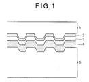
- a read-only optical disc has a structure as shown in FIG. 1 , in which data are recorded as convex and concave pits on a transparent plastic substrate during the manufacture of the disc, and a reflective layer is formed typically from Al, Ag or Au thereon. The recorded data are reproduced (read out) by detecting a difference in phase or reflection of laser light applied to the disc.
- Certain optical discs each containing laminated two substrates have two recording layers. One of the two substrates has recording pits and is covered by a reflective layer, and the other has different recording pits and is covered by a semi-reflective layer.
- the data according to this writing/reading system namely, single side, dual layer system, are read-only and can be neither rewritten nor changed.
- FIG. 1 is a schematic cross sectional view of an optical disc.
- the optical disc includes a polycarbonate substrate 1, a semi-reflective layer 2 made typically of Au, Ag alloy or Si, an adhesive layer 3, a reflective layer 4 made typically of a Ag alloy, and a protective layer 5 made typically from an ultraviolet curable resin.
- Such read-only optical discs cannot significantly have a respective identification (ID), since these discs are produced in a large quantity where information to be written is pressed on the discs using a stamper during their manufacture.
- Read-only optical discs having a respective identification have been developed for preventing illegal duplication, improving the traceability during commercial distribution and increasing added values of the discs.
- the identification (ID) is recorded on the discs according to, for example, a Label Gate system or burst cutting area (BCA) system with a dedicated apparatus after the manufacture of the discs.
- the ID is generally marked by irradiating laser beam to a disc after its manufacture, thereby melting and puncturing the A1 alloy of the reflective film.
- Such reflective films of read-only optical discs have generally been prepared from Al alloys such as an Al alloy according to the specification in Japanese Industrial Standards (JIS) A 6061 (Al-Mg alloy). Such Al alloys are widely distributed as a general-purpose constitutional material and are thereby inexpensive.
- JIS Japanese Industrial Standards
- Al-Mg alloy Al-Mg alloy
- TheAl alloy according to JISA 6061 is not directed to laser marking process and has the following problems.
- the Al alloy according to JIS A 6061 has a high thermal conductivity and thus requires a high laser power for marking, which invites damage, for example, on the polycarbonate substrate or the adhesive layer.
- the alloy has low corrosion resistance, has cavities as a result of the laser marking, and the resulting reflective film cannot avoid corrosion after laser marking.
- the corrosion resistance herein can be determined in a test with constant temperature and humidity.
- Recordable optical discs such as write-once optical discs and rewritable optical discs generally employ Ag alloys for their higher reflectivity.
- a reflective film made from a Ag alloy is susceptible to cohesion at high temperatures due to its low heat resistance.
- Various proposals have been made to avoid this problem and to improve the durability of such a Ag alloy.
- Japanese Patent Application Laid-open No. 2002-15464 discloses prevention of growth of crystal grain (cohesion) of Ag by adding 0.1 to 3 atomic percent of a rare earth element to Ag.
- Japanese Patent Application Laid-open No. 2004-139712 disclosesimprovementin reflectivity and durability while maintaining high thermal conductivity by incorporating Bi or Sb into Ag.
- the thermal conductivity of the Ag alloy is reduced in Japanese Patent Application Laid-open No. 04-25440 and No. 04-28032 by adding an alloying element to Ag. These reflective films, however, are not directed to laser marking in which the film is melted and removed by laser irradiation. Accordingly, no Ag alloy has been provided to have a reduced thermal conductivity and a reduced melting temperature simultaneously to thereby satisfy requirements as a Ag alloy for use in laser marking.
- a Ag alloy for use in laser marking must have a low thermal conductivity, low melting temperature, high corrosion resistance and high heat resistance.
- the Al alloy according to JIS A 6061 generally used in read-only optical discs cannot be used in laser marking due to its high thermal conductivity and low corrosion resistance.
- a Ag alloy thin film containing a specific amount of at least one specific alloying element in addition to Ag has a low thermal conductivity, low melting temperature and high corrosion resistance and is suitable for use in laser marking as a reflective thin film layer (metal thin film layer) for an optical information recording medium.
- the present invention has been achieved based on these findings.
- the present invention relates to a Ag alloy reflective film for an optical information recording medium, an optical information recording medium, and a Ag alloy sputtering target for the deposition of Ag alloy reflective film having the following configurations.
- the present invention provides, in a first aspect, a Ag alloy reflective film for an optical information recording medium, containing Ag as a main component, and at least one selected from the group consisting of Nd, Sn, Gd and In in a total amount of more than 3.0 atomic percent and less than or equal to 10 atomic percent.
- the Ag alloy reflective film can further contain 0.01 to 3 atomic percent of at least one of Bi and Sb.
- the Ag alloy reflective film can further contain 20 atomic percent or less of at least one selected from the group consisting of Mn, Cu, La and Zn.
- the present invention further provides, in a second aspect, an optical information recording medium having the Ag alloy reflective film of the present invention.
- the optical information recording medium can be subjected to laser marking.
- the present invention provides a Ag alloy sputtering target for the deposition of a Ag alloy reflective film, containing Ag as a main component, and at least one selected from the group consisting of Nd, Sn, Gd and In in a total amount of more than 3.0 atomic percent and less than or equal to 10 atomic percent.
- the Ag alloy sputtering target can further contain 0.01 to 3 atomic percent of Sb.
- the Ag alloy sputtering target can further contain 0.03 to 10 atomic percent of Bi.
- the Ag alloy reflective film can contain 20 atomic percent or less of at least one selected from the group consisting of Mn, Cu, La and Zn.
- the Ag alloy reflective film for an optical information recording medium according to the present invention enables easy laser marking on a read-only optical disc.
- the optical information recording medium according to the present invention has the Ag alloy reflective film and enables easy laser marking when used as a read-only optical disc.
- the Ag alloy sputtering target according to the present invention enables the deposition of such a Ag alloy reflective film.
- FIG. 1 is a schematic sectional view of a configuration of a read-only optical disc.
- a Ag alloy for use in laser marking must have a low thermal conductivity, low melting temperature and high corrosion resistance.
- the present inventors prepared Ag alloy sputtering targets by adding various elements to Ag, prepared Ag alloy thin films having different compositions by sputtering using these targets, determined their compositions and properties as reflective thin films and found the following findings (1), (2) and (3).
- the present invention has been achieved based on these findings and provides the Ag alloy reflective film for an optical information recordingmedium, the optical information recording medium, and the Ag alloy sputtering target for the deposition of the Ag alloy reflective film having the above configurations.
- the Ag alloy reflective film according to the first embodiment of the present invention is for use in an optical information recording medium, mainly comprises Ag and further comprises at least one of Nd, Sn, Gd and In in a total content of more than 3.0 atomic percent and equal to or less than 10 atomic percent.
- the Ag alloy reflective film can have a reduced thermal conductivity and improved durability without elevating its melting temperature (liquidus temperature) by comprising at least one of Nd, Sn, Gd and In in a total content of more than 3.0 atomic percent and equal to or less than 10 atomic percent as described in the finding (1).
- the Ag alloy reflective film according to the present invention therefore has a low thermal conductivity, low melting temperature and high corrosion resistance, can be suitably used in laser marking and can be advantageously used as a reflective film for an optical information recording medium. More specifically, the low melting temperature of the Ag alloy reflective film enables easy laser marking. The low thermal conductivity thereof does not require excessive laser output and reduces the laser output in the laser marking, which in turn avoids thermal damage of constitutional members of the disc such as polycarbonate substrate and adhesive layer due to excessive laser output. In addition, the high corrosion resistance prevents the decreased reflectivity due to corrosion or cohesion caused by water migrated into cavities formed after laser marking.
- the Ag alloy reflective film according to the second embodiment significantly prevents the decreased reflectivity due to corrosion or cohesion in the test with constant temperature and humidity, as described in the finding (2).
- the Ag alloy reflective film according to the third embodiment can have a further reduced thermal conductivity, as described in the finding (3).
- the thickness of the Ag alloy reflective film is preferably 10 nm to 200 nm, and more preferably 20 nm to 100 nm. If the thickness is less than 10 nm, the reflective film may transmit light and have a decreased reflectivity, although such a thin film is advantageous for laser marking.
- the thickness of the reflective film is thus preferably 10 nm or more and more preferably 20 nm or more.
- the thickness is preferably 200 nm or less, and more preferably 100 nm or less, because a Ag alloy reflective film having an excessively large thickness may require a larger energy for laser marking so as to fuse the reflective film.
- the reflective film may have a decreased surface smoothness, may scatter light more and fail to obtain a high signal output.
- the optical information recording medium according to the present invention comprises the Ag alloy reflective film of the present invention.
- the optical information recording medium can be suitably subjected to laser marking, is free from thermal damage of constitutional members thereof, such as the polycarbonate substrate and adhesive layer, due to excessive laser output.
- the optical information recording medium has high corrosion resistance and is resistant to the decreased reflectivity due to corrosion or cohesion.
- optical information recording medium according to the present invention has such satisfactory properties and can be particularly advantageously used in laser marking.
- the Ag alloy sputtering target for the deposition of a Ag alloy reflective film according to the present invention mainly comprises Ag and further comprises at least one selected from the group consisting of Nd, Sn, Gd and In in a total amount of more than 3.0 atomic percent and less than or equal to 10 atomic percent.
- the Ag alloy sputtering target enables the deposition of the Ag alloy reflective film for an optical information recording medium accordingto the present invention.
- the Ag alloy sputtering target enables the deposition of the Ag alloy reflective film according to the second embodiment, wherein the Ag alloy reflective film comprises 0.01 to 3 atomic percent of Sb.
- the Ag alloy sputtering target further comprises 0.03 to 10 atomic percent of Bi, it enables the deposition of the Ag alloy reflective film according to the second embodiment, wherein the Ag alloy reflective film comprises 0.01 to 3 atomic percent of Bi.
- the Bi content in the target is higher than the Bi content in the reflective film since the amount of Bi in the resulting reflective film reduces to several dozen percent of the Bi that had been present in the target in the course of depositing the reflective film.
- the content of the Nd, Sn, G, In or Sb in the target is substantially equal to the content in the resulting reflective film.
- the Ag alloy sputtering target enables the deposition of the Ag alloy reflective film according to the third embodiment of the present invention.
- the content of the Nd, Sn, Gd or In in the target is substantially equal to the content in the resulting reflective film.
- Thin films of Ag-Nd (Nd-containing Ag alloy), Ag-Sn (Sn-containing Ag alloy), Ag-Gd (Gd-containing Ag alloy), Ag-In (In-containing Ag alloy) and Ag-Nd-Sn (Nd-Sn-containing Ag alloy) were prepared, and the relationships between the contents of Nd, Sn, Gd and In, and the melting temperature, thermal conductivity and reflectivity of the thin films were determined.
- the thin films were prepared in the following manner. On a glass substrate (Corning #1737 having a diameter of 50 mm and a thickness of 1 mm) were deposited thin films of Ag-Nd, Ag-Sn, Ag-Gd, Ag-In and Ag-Nd-Sn with a DC magnetron sputter at a substrate temperature of 22°C, an Ar gas pressure of 2 mTorr, a deposition rate of 5 nm/sec and a base pressure of less than 5 ⁇ 10 -6 Torr.
- the sputtering target was a composite target comprising a pure Ag target and chips of an alloying element arranged on the pure Ag target.
- the melting temperature of a sample thin film was determined in the following manner.
- a sample Ag alloy thin film 1 ⁇ m thick (the Ag-Nd thin film, the Ag-Sn thin film, the Ag-Gd thin film, the Ag-In thin film or the Ag-Nd-Sn thin film) was stripped from the substrate, and about 5 mg of the stripped thin film was subjected to measurement with a differential calorimeter.
- the melting temperature of the sample thin film was defined as the average of a temperature at which the thin film was completely fused in the course of temperature rise, and a temperature at which the thin film began to solidify in the course of temperature fall.
- the thermal conductivity was determined by converting from the electric resistivity of a sample Ag alloy thin film 100 nm thick.
- the reflectivity of a sample Ag alloy thin film was determined at a wavelength of 405 nm after the deposition of the thin film and after a test with constant temperature and humidity (environmental test).
- the test with constant temperature and humidity (environmental test) was carried out at a temperature of 80°C and relative humidity (RH) of 90% for hundred hours.
- Ag-x ⁇ Nd represents a Ag alloy containing x atomic percent of Nd (Ag-Nd alloy)
- Ag-y ⁇ Sn represents a Ag alloy containing y atomic percent of Sn (Ag-Sn alloy)
- Ag-z ⁇ Gd represents a Ag alloy containing z atomic percent of Gd (Ag-Gd alloy)
- Ag-w ⁇ In represents a Ag alloy containing w atomic percent of In (Ag-In alloy).
- Ag-5.0Nd for example, represents a Ag alloy containing 5.0 atomic percent of Nd.
- Table 1 shows that the thermal conductivity and the melting temperature decrease with decreasing contents of Nd, Sn, Gd and In.
- the thin films containing these elements in a total content of 3.0 atomic percent or less fail to exhibit a sufficiently low thermal conductivity.
- the thin films containing these elements in a total content of more than 10 atomic percent fail to exhibit a sufficiently high reflectivity.
- the total amount (total content) of Nd, Sn, Gd and In should be more than 3.0 atomic percent and equal to or less than 10 atomic percent and is preferably from 3.2 to 8 atomic percent.
- Thin films of Ag-5.0Nd-Bi (thin films of Ag alloys each containing 5.0 atomic percent of Nd and a certain amount of Bi) and thin films of Ag-5.0Nd-Sb (thin films of Ag alloys each containing 5.0 atomic percent of Nd and a certain amount of Sb) were prepared, and the relationships between the content of Bi or Sb and the thermal conductivity and reflectivity of the thin films were determined.
- the thin films were prepared in the following manner. On a glass substrate (Corning #1737 having a diameter of 50 mm and a thickness of 1 mm) were deposited thin films of Ag-5.0Nd-Bi and Ag-5.0Nd-Sb with a DC magnetron sputter at a substrate temperature of 22°C, an Ar gas pressure of 2 mTorr, a deposition rate of 5 nm/sec and a base pressure of less than 5 ⁇ 10 -6 Torr.
- the sputtering target was a composite target comprising a pure Ag target and chips of an alloying element arranged on the pure Ag target.
- the thermal conductivity was determined by converting from the electric resistivity of a sample Ag alloy thin film 100 nm thick.
- the reflectivity of a sample Ag alloy thin film was determined at a wavelength of 405 nm after the deposition of the thin film and after the test with constant temperature and humidity (environmental test) at a temperature of 80°C and relative humidity (RH) of 90% for hundred hours.
- the Bi content in theAg-5.0Nd-Bi thin films and the Sb content in theAg-5.0Nd-Sb thin films in the column of the composition are each expressed as an atomic percent.
- “Ag-5.0Nd-a Bi” represents a Ag alloy containing 5.0 atomic percent of Nd and a atomic percent of Bi (Ag-Nd-Bi alloy).
- “Ag-5.0Nd-1.0Bi” represents a Ag alloy containing 5.0 atomic percent of Nd and 1.0 atomic percent of Bi.
- Table 2 shows that the addition of Bi or Sb prevents the reflectivity from decreasing after the environmental test (decreased reflectivity due to corrosion or cohesion in the test with constant temperature and humidity).
- the reflectivity is not effectively prevented from decreasing at a content of these elements of less than 0.01 atomic percent but is effectively prevented at a content of these elements of 0.01 atomic percent or more.
- the reflectivity of the thin films decreases with an increasing content of Bi and/or Sb and is very low at a content of Bi and/Sb of more than 3.0 atomic percent.
- the content of Bi and/or Sb is preferably 0.01 to 3.0 atomic percent based on these results.
- Thin films of Ag-3.2Nd-(La,Mn,Cu,Zn) (thin films of Ag alloys each containing 3.2 atomic percent of Nd and a certain amount of one of La, Mn, Cu and Zn) and thin films of Ag-1.0Nd-5.0Sn-Cu (thin films of Ag alloys each containing 1.0 atomic percent of Nd, 5.0 atomic percent of Sn and a certain amount of Cu) were prepared, and the relationships between the content of La, Mn, Cu or Zn and the melting temperature, thermal conductivity and reflectivity of the thin films were determined.
- the thin films were prepared in the following manner. On a glass substrate (Corning #1737 having a diameter of 50 mm and a thickness of 0.7 mm) were deposited thin films of Ag-3.2Nd-(La,Mn,Cu,Zn) and Ag-1.0Nd-5.0Sn-Cu with a DC magnetron sputter under the same condition as Experimental Example 2.
- the sputtering target was a composite target comprising a pure Ag target and chips of an alloying element arranged on the pure Ag target.
- the melting temperature of a sample thin film was determined in the following manner. A sample Ag alloy thin film 1 ⁇ m thick was stripped from the substrate, and about 5 mg of the stripped thin film was subjected to measurement with a differential calorimeter. The melting temperature of the sample thin film was defined as the average of a temperature at which the thin film was completely fused in the course of temperature rise, and a temperature at which the thin film began to solidify in the course of temperature fall. The thermal conductivity was determined by converting from the electric resistivity of a sample Ag alloy thin film 100 nm thick. The reflectivity of a sample Ag alloy thin film was determined at a wavelength of 405 nm.
- Table 3 shows that the thermal conductivity significantly decreases with the addition of La, Mn, Cu or Zn.
- the reflectivity of the thin film decreases with an increasing content of these elements and is very low at a content of these elements of more than 20 atomic percent.
- the samples in the above experimental examples comprise either one of Nd, Sn, Gd and In, or a combination of Nd and Sn.
- the samples comprise either one of Bi and Sb, and/or either one of La, Mn, Cu and Zn. Similar results to above are obtained by incorporating other combinations of two or more of Nd, Sn, Gd and In, by incorporating both Bi and Sb, and by incorporating two or more of La, Mn, Cu and Zn.
- the Ag alloy reflective film for an optical information recording medium according to the present invention enables easy laser marking in read-only optical discs and can be suitably used as a reflective film for an optical information recording medium serving as a read-only optical disc.
Abstract
Description
- The present invention relates to an Ag alloy reflective film for an optical information recording medium; an optical information recording medium using the Ag alloy reflective film, and an Ag alloy sputtering target for the deposition of the Ag alloy reflective film. More specifically, it relates to a reflective film which exhibits a low thermal conductivity, low melting point, high reflectivity and high corrosion resistance for enabling laser marking after the preparation of a disc in the field of optical information recording media such as compact disc (CD), digital versatile disc (DVD), Blu-ray Disc, and high definition DVD (HD DVD) It also relates to a sputtering target which is used in depositing the reflective film; and an optical information recording medium having the reflective film.
- Optical information recording media (optical discs) include various types, and the three main types categorized by the writing/reading system are read-only, write-once, and rewritable optical discs.
- Of these optical discs, a read-only optical disc has a structure as shown in
FIG. 1 , in which data are recorded as convex and concave pits on a transparent plastic substrate during the manufacture of the disc, and a reflective layer is formed typically from Al, Ag or Au thereon. The recorded data are reproduced (read out) by detecting a difference in phase or reflection of laser light applied to the disc. Certain optical discs each containing laminated two substrates have two recording layers. One of the two substrates has recording pits and is covered by a reflective layer, and the other has different recording pits and is covered by a semi-reflective layer. The data according to this writing/reading system, namely, single side, dual layer system, are read-only and can be neither rewritten nor changed. Examples of such optical discs according to this writing/reading system are CD-ROM and DVD-ROM.FIG. 1 is a schematic cross sectional view of an optical disc. The optical disc includes apolycarbonate substrate 1, a semi-reflective layer 2 made typically of Au, Ag alloy or Si, an adhesive layer 3, areflective layer 4 made typically of a Ag alloy, and aprotective layer 5 made typically from an ultraviolet curable resin. - Such read-only optical discs cannot significantly have a respective identification (ID), since these discs are produced in a large quantity where information to be written is pressed on the discs using a stamper during their manufacture. Read-only optical discs having a respective identification, however, have been developed for preventing illegal duplication, improving the traceability during commercial distribution and increasing added values of the discs. The identification (ID) is recorded on the discs according to, for example, a Label Gate system or burst cutting area (BCA) system with a dedicated apparatus after the manufacture of the discs. The ID is generally marked by irradiating laser beam to a disc after its manufacture, thereby melting and puncturing the A1 alloy of the reflective film.
- Such reflective films of read-only optical discs have generally been prepared from Al alloys such as an Al alloy according to the specification in Japanese Industrial Standards (JIS) A 6061 (Al-Mg alloy). Such Al alloys are widely distributed as a general-purpose constitutional material and are thereby inexpensive.
- TheAl alloy according to JISA 6061, however, is not directed to laser marking process and has the following problems.
- The Al alloy according to JIS A 6061 has a high thermal conductivity and thus requires a high laser power for marking, which invites damage, for example, on the polycarbonate substrate or the adhesive layer. In addition, the alloy has low corrosion resistance, has cavities as a result of the laser marking, and the resulting reflective film cannot avoid corrosion after laser marking. The corrosion resistance herein can be determined in a test with constant temperature and humidity.
- Recordable optical discs such as write-once optical discs and rewritable optical discs generally employ Ag alloys for their higher reflectivity. A reflective film made from a Ag alloy, however, is susceptible to cohesion at high temperatures due to its low heat resistance. Various proposals have been made to avoid this problem and to improve the durability of such a Ag alloy. For example, Japanese Patent Application Laid-open No.
2002-15464 2004-139712 - The thermal conductivity of the Ag alloy is reduced in Japanese Patent Application Laid-open No.
04-25440 04-28032 - As is described above, a Ag alloy for use in laser marking must have a low thermal conductivity, low melting temperature, high corrosion resistance and high heat resistance.
- The Al alloy according to JIS A 6061 generally used in read-only optical discs cannot be used in laser marking due to its high thermal conductivity and low corrosion resistance.
- Under these circumstances, an object of the present invention is to provide a Ag alloy reflective film for an optical information recording medium, which enables easy laser marking on a read-only optical disc. Another object of the present invention is to provide an optical information recording medium having the reflective film. Yet another object of the present invention is to provide a sputtering target for the deposition of the reflective film.
- After intensive investigations to achieve the above objects, the present inventors have found that a Ag alloy thin film containing a specific amount of at least one specific alloying element in addition to Ag has a low thermal conductivity, low melting temperature and high corrosion resistance and is suitable for use in laser marking as a reflective thin film layer (metal thin film layer) for an optical information recording medium. The present invention has been achieved based on these findings.
- Accordingly, the present invention relates to a Ag alloy reflective film for an optical information recording medium, an optical information recording medium, and a Ag alloy sputtering target for the deposition of Ag alloy reflective film having the following configurations.
- Specifically, the present invention provides, in a first aspect, a Ag alloy reflective film for an optical information recording medium, containing Ag as a main component, and at least one selected from the group consisting of Nd, Sn, Gd and In in a total amount of more than 3.0 atomic percent and less than or equal to 10 atomic percent.
- The Ag alloy reflective film can further contain 0.01 to 3 atomic percent of at least one of Bi and Sb.
- In addition or alternatively, the Ag alloy reflective film can further contain 20 atomic percent or less of at least one selected from the group consisting of Mn, Cu, La and Zn.
- The present invention further provides, in a second aspect, an optical information recording medium having the Ag alloy reflective film of the present invention.
- The optical information recording medium can be subjected to laser marking.
- In addition and advantageously, the present invention provides a Ag alloy sputtering target for the deposition of a Ag alloy reflective film, containing Ag as a main component, and at least one selected from the group consisting of Nd, Sn, Gd and In in a total amount of more than 3.0 atomic percent and less than or equal to 10 atomic percent.
- The Ag alloy sputtering target can further contain 0.01 to 3 atomic percent of Sb.
- The Ag alloy sputtering target can further contain 0.03 to 10 atomic percent of Bi.
- In addition or alternatively, the Ag alloy reflective film can contain 20 atomic percent or less of at least one selected from the group consisting of Mn, Cu, La and Zn.
- The Ag alloy reflective film for an optical information recording medium according to the present invention enables easy laser marking on a read-only optical disc. The optical information recording medium according to the present invention has the Ag alloy reflective film and enables easy laser marking when used as a read-only optical disc. The Ag alloy sputtering target according to the present invention enables the deposition of such a Ag alloy reflective film.
- Further objects, features and advantages of the present invention will become apparent from the following description of the preferred embodiments with reference to the attached drawing.
-
FIG. 1 is a schematic sectional view of a configuration of a read-only optical disc. - As is described above, a Ag alloy for use in laser marking must have a low thermal conductivity, low melting temperature and high corrosion resistance.
- The present inventors prepared Ag alloy sputtering targets by adding various elements to Ag, prepared Ag alloy thin films having different compositions by sputtering using these targets, determined their compositions and properties as reflective thin films and found the following findings (1), (2) and (3).
- (1) The thermal conductivity can be reduced without elevating the melting temperature (liquidus temperature) by adding to Ag at least one, namely one or more elements selected from Nd, Sn, Gd and In in a total amount of more than 3.0 atomic percent and equal to or less than 10 atomic percent. If the total amount of the at least one element is 3.0 atomic percent (hereinafter briefly referred to as percent or %) or less, the thermal conductivity is not effectively reduced. If it exceeds 10 atomic percent, the reflectivity significantly decreases. By adding more than 3 atomic percent and equal to or less than 10 atomic percent of at least one of these elements, the resulting reflective film can have a reduced thermal conductivity and melting temperature and exhibit improved durability. More specifically, the reflective film is resistant to corrosion and cohesion and prevents decrease in reflectivity under high temperature and high humidity conditions in a test with constant temperature and humidity after laser marking (hereinafter referred to as "decreased reflectivity due to corrosion or cohesion in the test with constant temperature and humidity").
- (2) The decreased reflectivity due to corrosion or cohesion in the test with constant temperature and humidity can be significantly prevented by further adding at least one of Bi and Sb in addition to at least one selected from Nd, Sn, Gd and In in the specific amount. The total content of Bi and/or Sb is preferably 3 atomic percent or less for preventing, as a result of alloying, decrease in reflectivity. It is also preferably 0.01 atomic percent for satisfactory effects of the alloying. The total content of Bi and Sb is more preferably 0.1 atomic percent or more and 2.0 atomic percent or less.
- (3) The thermal conductivity can be significantly reduced by further adding at least one of Mn, Cu, La and Zn. The total content of these elements is preferably 20 atomic percent or less for preventing, as a result of alloying, decrease in reflectivity. These elements, however, do not significantly contribute to improvement in the durability of the resulting reflective film. For further effectively reducing the thermal conductivity, the total content of these elements is preferably 0.1 atomic percent or more and more preferably 1.0 atomic percent or more.
- The present invention has been achieved based on these findings and provides the Ag alloy reflective film for an optical information recordingmedium, the optical information recording medium, and the Ag alloy sputtering target for the deposition of the Ag alloy reflective film having the above configurations.
- Thus, the Ag alloy reflective film according to the first embodiment of the present invention is for use in an optical information recording medium, mainly comprises Ag and further comprises at least one of Nd, Sn, Gd and In in a total content of more than 3.0 atomic percent and equal to or less than 10 atomic percent.
- The Ag alloy reflective film can have a reduced thermal conductivity and improved durability without elevating its melting temperature (liquidus temperature) by comprising at least one of Nd, Sn, Gd and In in a total content of more than 3.0 atomic percent and equal to or less than 10 atomic percent as described in the finding (1).
- The Ag alloy reflective film according to the present invention therefore has a low thermal conductivity, low melting temperature and high corrosion resistance, can be suitably used in laser marking and can be advantageously used as a reflective film for an optical information recording medium. More specifically, the low melting temperature of the Ag alloy reflective film enables easy laser marking. The low thermal conductivity thereof does not require excessive laser output and reduces the laser output in the laser marking, which in turn avoids thermal damage of constitutional members of the disc such as polycarbonate substrate and adhesive layer due to excessive laser output. In addition, the high corrosion resistance prevents the decreased reflectivity due to corrosion or cohesion caused by water migrated into cavities formed after laser marking.
- By further comprising 0.01 to 3 atomic percent of at least one of Bi and Sb, the Ag alloy reflective film according to the second embodiment significantly prevents the decreased reflectivity due to corrosion or cohesion in the test with constant temperature and humidity, as described in the finding (2).
- By further comprising 20 atomic percent or less of at least one of Mn, Cu, La and Zn, the Ag alloy reflective film according to the third embodiment can have a further reduced thermal conductivity, as described in the finding (3).
- The thickness of the Ag alloy reflective film is preferably 10 nm to 200 nm, and more preferably 20 nm to 100 nm. If the thickness is less than 10 nm, the reflective film may transmit light and have a decreased reflectivity, although such a thin film is advantageous for laser marking. The thickness of the reflective film is thus preferably 10 nm or more and more preferably 20 nm or more. In contrast, the thickness is preferably 200 nm or less, and more preferably 100 nm or less, because a Ag alloy reflective film having an excessively large thickness may require a larger energy for laser marking so as to fuse the reflective film. In addition, with an increasing thickness, the reflective film may have a decreased surface smoothness, may scatter light more and fail to obtain a high signal output.
- The optical information recording medium according to the present invention comprises the Ag alloy reflective film of the present invention. The optical information recording medium can be suitably subjected to laser marking, is free from thermal damage of constitutional members thereof, such as the polycarbonate substrate and adhesive layer, due to excessive laser output. In addition, the optical information recording medium has high corrosion resistance and is resistant to the decreased reflectivity due to corrosion or cohesion.
- The optical information recording medium according to the present invention has such satisfactory properties and can be particularly advantageously used in laser marking.
- The Ag alloy sputtering target for the deposition of a Ag alloy reflective film according to the present invention mainly comprises Ag and further comprises at least one selected from the group consisting of Nd, Sn, Gd and In in a total amount of more than 3.0 atomic percent and less than or equal to 10 atomic percent. The Ag alloy sputtering target enables the deposition of the Ag alloy reflective film for an optical information recording medium accordingto the present invention.
- By further comprising 0.01 to 3 atomic percent of Sb, the Ag alloy sputtering target enables the deposition of the Ag alloy reflective film according to the second embodiment, wherein the Ag alloy reflective film comprises 0.01 to 3 atomic percent of Sb. When the Ag alloy sputtering target further comprises 0.03 to 10 atomic percent of Bi, it enables the deposition of the Ag alloy reflective film according to the second embodiment, wherein the Ag alloy reflective film comprises 0.01 to 3 atomic percent of Bi. The Bi content in the target is higher than the Bi content in the reflective film since the amount of Bi in the resulting reflective film reduces to several dozen percent of the Bi that had been present in the target in the course of depositing the reflective film. In this connection, the content of the Nd, Sn, G, In or Sb in the target is substantially equal to the content in the resulting reflective film.
- By further comprising 20 atomic percent or less of at least one of Mn, Cu, La and Zn, the Ag alloy sputtering target enables the deposition of the Ag alloy reflective film according to the third embodiment of the present invention. The content of the Nd, Sn, Gd or In in the target is substantially equal to the content in the resulting reflective film.
- The present invention will be described in further detail by referring to the following examples and comparative examples which by no means limit the scope of the present invention. Any modification of such examples without deviating the scope of the present invention is within the technical range of the present invention.
- Thin films of Ag-Nd (Nd-containing Ag alloy), Ag-Sn (Sn-containing Ag alloy), Ag-Gd (Gd-containing Ag alloy), Ag-In (In-containing Ag alloy) and Ag-Nd-Sn (Nd-Sn-containing Ag alloy) were prepared, and the relationships between the contents of Nd, Sn, Gd and In, and the melting temperature, thermal conductivity and reflectivity of the thin films were determined.
- The thin films were prepared in the following manner. On a glass substrate (Corning #1737 having a diameter of 50 mm and a thickness of 1 mm) were deposited thin films of Ag-Nd, Ag-Sn, Ag-Gd, Ag-In and Ag-Nd-Sn with a DC magnetron sputter at a substrate temperature of 22°C, an Ar gas pressure of 2 mTorr, a deposition rate of 5 nm/sec and a base pressure of less than 5×10⁻⁶ Torr. The sputtering target was a composite target comprising a pure Ag target and chips of an alloying element arranged on the pure Ag target.
- The melting temperature of a sample thin filmwas determined in the following manner. A sample Ag alloy
thin film 1 µm thick (the Ag-Nd thin film, the Ag-Sn thin film, the Ag-Gd thin film, the Ag-In thin film or the Ag-Nd-Sn thin film) was stripped from the substrate, and about 5 mg of the stripped thin film was subjected to measurement with a differential calorimeter. The melting temperature of the sample thin film was defined as the average of a temperature at which the thin film was completely fused in the course of temperature rise, and a temperature at which the thin film began to solidify in the course of temperature fall. The thermal conductivity was determined by converting from the electric resistivity of a sample Ag alloy thin film 100 nm thick. The reflectivity of a sample Ag alloy thin film was determined at a wavelength of 405 nm after the deposition of the thin film and after a test with constant temperature and humidity (environmental test). The test with constant temperature and humidity (environmental test) was carried out at a temperature of 80°C and relative humidity (RH) of 90% for hundred hours. - The results are shown in Table 1. In Table 1, the contents of Nd, Sn, Gd, In in the Ag-Nd, Ag-Sn, Ag-Gd, Ag-In, and Ag-Nd-Sn thin films in the column of the composition are each expressed as an atomic percent. Specifically, "Ag-x·Nd" represents a Ag alloy containing x atomic percent of Nd (Ag-Nd alloy) ; "Ag-y·Sn" represents a Ag alloy containing y atomic percent of Sn (Ag-Sn alloy); "Ag-z·Gd" represents a Ag alloy containing z atomic percent of Gd (Ag-Gd alloy) ; and "Ag-w·In" represents a Ag alloy containing w atomic percent of In (Ag-In alloy). "Ag-5.0Nd", for example, represents a Ag alloy containing 5.0 atomic percent of Nd.
- Table 1 shows that the thermal conductivity and the melting temperature decrease with decreasing contents of Nd, Sn, Gd and In.
- The thin films containing these elements in a total content of 3.0 atomic percent or less fail to exhibit a sufficiently low thermal conductivity. The thin films containing these elements in a total content of more than 10 atomic percent fail to exhibit a sufficiently high reflectivity.
- These results show that the total amount (total content) of Nd, Sn, Gd and In should be more than 3.0 atomic percent and equal to or less than 10 atomic percent and is preferably from 3.2 to 8 atomic percent.
- Thin films of Ag-5.0Nd-Bi (thin films of Ag alloys each containing 5.0 atomic percent of Nd and a certain amount of Bi) and thin films of Ag-5.0Nd-Sb (thin films of Ag alloys each containing 5.0 atomic percent of Nd and a certain amount of Sb) were prepared, and the relationships between the content of Bi or Sb and the thermal conductivity and reflectivity of the thin films were determined.
- The thin films were prepared in the following manner. On a glass substrate (Corning #1737 having a diameter of 50 mm and a thickness of 1 mm) were deposited thin films of Ag-5.0Nd-Bi and Ag-5.0Nd-Sb with a DC magnetron sputter at a substrate temperature of 22°C, an Ar gas pressure of 2 mTorr, a deposition rate of 5 nm/sec and a base pressure of less than 5×10⁻⁶ Torr. The sputtering target was a composite target comprising a pure Ag target and chips of an alloying element arranged on the pure Ag target.
- The thermal conductivity was determined by converting from the electric resistivity of a sample Ag alloy thin film 100 nm thick. The reflectivity of a sample Ag alloy thin film was determined at a wavelength of 405 nm after the deposition of the thin film and after the test with constant temperature and humidity (environmental test) at a temperature of 80°C and relative humidity (RH) of 90% for hundred hours.
- The results are shown in Table 2. In Table 2, the Bi content in theAg-5.0Nd-Bi thin films and the Sb content in theAg-5.0Nd-Sb thin films in the column of the composition are each expressed as an atomic percent. Specifically, "Ag-5.0Nd-a Bi" represents a Ag alloy containing 5.0 atomic percent of Nd and a atomic percent of Bi (Ag-Nd-Bi alloy). "Ag-5.0Nd-1.0Bi", for example, represents a Ag alloy containing 5.0 atomic percent of Nd and 1.0 atomic percent of Bi.
- Table 2 shows that the addition of Bi or Sb prevents the reflectivity from decreasing after the environmental test (decreased reflectivity due to corrosion or cohesion in the test with constant temperature and humidity). The reflectivity is not effectively prevented from decreasing at a content of these elements of less than 0.01 atomic percent but is effectively prevented at a content of these elements of 0.01 atomic percent or more.
- The reflectivity of the thin films decreases with an increasing content of Bi and/or Sb and is very low at a content of Bi and/Sb of more than 3.0 atomic percent.
- The content of Bi and/or Sb is preferably 0.01 to 3.0 atomic percent based on these results.
- Thin films of Ag-3.2Nd-(La,Mn,Cu,Zn) (thin films of Ag alloys each containing 3.2 atomic percent of Nd and a certain amount of one of La, Mn, Cu and Zn) and thin films of Ag-1.0Nd-5.0Sn-Cu (thin films of Ag alloys each containing 1.0 atomic percent of Nd, 5.0 atomic percent of Sn and a certain amount of Cu) were prepared, and the relationships between the content of La, Mn, Cu or Zn and the melting temperature, thermal conductivity and reflectivity of the thin films were determined.
- The thin films were prepared in the following manner. On a glass substrate (Corning #1737 having a diameter of 50 mm and a thickness of 0.7 mm) were deposited thin films of Ag-3.2Nd-(La,Mn,Cu,Zn) and Ag-1.0Nd-5.0Sn-Cu with a DC magnetron sputter under the same condition as Experimental Example 2. The sputtering target was a composite target comprising a pure Ag target and chips of an alloying element arranged on the pure Ag target.
- The melting temperature of a sample thin film was determined in the following manner. A sample Ag alloy
thin film 1 µm thick was stripped from the substrate, and about 5 mg of the stripped thin film was subjected to measurement with a differential calorimeter. The melting temperature of the sample thin film was defined as the average of a temperature at which the thin film was completely fused in the course of temperature rise, and a temperature at which the thin film began to solidify in the course of temperature fall. The thermal conductivity was determined by converting from the electric resistivity of a sample Ag alloy thin film 100 nm thick. The reflectivity of a sample Ag alloy thin film was determined at a wavelength of 405 nm. - The results are shown in Table 3. In Table 3, the contents of La, Mn, Cu and Zn in the Ag-3.2Nd-(La,Mn,Cu,Zn) thin films and the Cu content in the Ag-1.0Nd-5.0Sn-Cu thin films in the column of the composition are each expressed as an atomic percent. Specifically, "Ag-3.2Nd-b·La (or Mn, Cu or Zn)" represents a Ag alloy containing 3.2 atomic percent of Nd and b atomic percent of La (or Mn, Cu or Zn) [Ag-Nd-(La,Mn,Cu,Zn) alloy]. "Ag-3.2Nd-5.0La", for example, represents a Ag alloy containing 3.2 atomic percent of Nd and 5.0 atomic percent of La.
- Table 3 shows that the thermal conductivity significantly decreases with the addition of La, Mn, Cu or Zn. The reflectivity of the thin film decreases with an increasing content of these elements and is very low at a content of these elements of more than 20 atomic percent.
- These results show that the total content of La, Mn, Cu and Zn is preferably 20 atomic percent or less.
Table 1 Composition Melting temperature (°C) Electric resistivity (µΩcm) Thermal conductivity (W/ (cm·K)) Reflectivity (%) After deposition After environmental test pure Ag 960 2.4 3.2 93.2 70.2 Ag-0.5Nd 958 4.8 1.57 90.4 85.3 Ag-1.0Nd 955 7.3 1.03 87.0 84.3 Ag-5.0Nd 910 26.9 0.28 75.7 70.3 Ag-10.0Nd 820 40.2 0.19 61.8 60.2 Ag-15.0Nd 920 76.2 0.10 55.2 50.3 Ag-0.1Sn 960 2.8 2.69 92.5 76.2 Ag-1.0Sn 957 7.1 1.06 88.2 85.2 Ag-5.0Sn 905 25.8 0.29 72.2 68.2 Ag-10.0Sn 860 38.2 0.20 65.2 61.2 Ag-15.0Sn 806 75.1 0.10 54.3 51.3 Ag-0.1Gd 958 3.2 2.35 92.8 72.3 Ag-1.0Gd 947 10.5 0.72 88.0 76.2 Ag-5.0Gd 887 43.6 0.17 74.1 63.2 Ag-10.0Gd 869 80.2 0.09 71.8 64.3 Ag-15.0Gd 902 101.1 0.07 58.3 53.2 Ag-0.01In 960 2.5 3.01 93.0 78.6 Ag-0. 1In 960 3.0 2.51 92.8 74.3 Ag-3.2In 944 21.3 0.35 82.3 76.6 Ag-10.0In 901 58.3 0.13 69.6 61.2 Ag-20.0In 831 110.2 0.07 44.3 48.6 Ag-1.0Nd-1.0Sn 942 12.4 0.60 84.1 78.5 Ag-1.0Nd-3.0sn 923 23.0 0.30 78.1 73.2 Ag-1.0Nd-5.0Sn 880 35.8 0.20 70.2 66.9 Ag-5.0Nd-10.0Sn 823 74.3 0.10 51.8 48.2 Table 2 Composition Electric resistivity (µΩcm) Thermal conductivity (W/ (cm·K)) Reflectivity (%) After deposition After environmental test pure Ag 2.4 3.2 93.2 70.2 Ag-5.0Nd 26.9 0.28 75.7 70.3 Ag-5.0Nd-0.005Bi 26.9 0.28 75.7 71.0 Ag-5.0Nd-0.01Bi 27.2 0.28 75.7 74.0 Ag-5.0Nd-1.0Bi 32.3 0.23 72.1 70.1 Ag-5.0Nd-3.0Bi 56.7 0.13 62.1 60.8 Ag-5.0Nd-5.0Bi 92.4 0.08 51.2 40.6 Ag-5.0Nd-0.005Sn 26.9 0.28 75.7 71.2 Ag-5.0Nd-0.01Sn 27.5 0.27 75.5 73.6 Ag-5.0Nd-1.0Sn 34.5 0.22 72.6 70.8 Ag-5.0Nd-3.0Sn 52.1 0.14 65.8 64.2 Ag-5.0Nd-5.0Sn 73.9 0.10 55.2 52.1 Table 3 Composition Melting temperatu re (°C) Electric resistivity (µΩcm) Therrmal conductivity (W/ (cm·K)) Reflectivity (%) pure Ag 960 2.4 3.14 93.2 Ag-3.2Nd-0.5La 932 21.6 0.35 81.2 Ag-3.2Nd-1.0La 931 23.7 0.32 79.8 Ag-3.2Nd-10.0La 812 72.3 0.10 68.5 Ag-3.2Nd-20.0La 865 98.2 0.08 62.1 Ag-3.2Nd-30.0La 921 121.6 0.06 52.4 Ag-3.2Nd-0.5Mn 931 14.1 0.53 81.0 Ag-3.2Nd-1.0Mn 931 16.1 0.47 78.0 Ag-3.2Nd-10.0Mn 964 30.1 0.25 70.2 Ag-3.2Nd-30.0Mn 971 47.1 0.16 56.9 Ag-3.2Nd-0.5Cu 928 15.0 0.50 90.1 Ag-3.2Nd-1.0Cu 920 16.2 0.46 88.2 Ag-3.2Nd-10.0Cu 870 20.3 0.37 73.4 Ag-3.2Nd-20.0Cu 842 30.2 0.25 65.2 Ag-3.2Nd-30.0Cu 786 52.1 0.14 59.1 Ag-3.2Nd-0.5Zn 945 13.0 0.58 82.0 Ag-3.2Nd-1.0Zn 945 13.4 0.56 81.6 Ag-3.2Nd-10.0Zn 910 18.3 0.41 78.2 Ag-3.2Nd-30.0Zn 765 23.8 0.32 58.8 Ag-1.0Nd-5.0Sn-2.0Cu 872 39.5 0.19 66.2 Ag-1.0Nd-5.0sn-5.0Cu 840 42.1 0.18 61.8 - The samples in the above experimental examples comprise either one of Nd, Sn, Gd and In, or a combination of Nd and Sn. Likewise, the samples comprise either one of Bi and Sb, and/or either one of La, Mn, Cu and Zn. Similar results to above are obtained by incorporating other combinations of two or more of Nd, Sn, Gd and In, by incorporating both Bi and Sb, and by incorporating two or more of La, Mn, Cu and Zn.
- The Ag alloy reflective film for an optical information recording medium according to the present invention enables easy laser marking in read-only optical discs and can be suitably used as a reflective film for an optical information recording medium serving as a read-only optical disc.
- While the present invention has been described with reference to what are presently considered to be the preferred embodiments, it is to be understood that the invention is not limited to the disclosed embodiments. On the contrary, the invention is intended to cover various modifications and equivalent arrangements included within the spirit and scope of the appended claims. The scope of the following claims is to be accorded the broadest interpretation so as to encompass all such modifications and equivalent structures and functions.
Claims (1)
- A read-only optical information recording medium for use in laser marking, comprising an Ag alloy reflective film, comprising:Ag as a main component, andat least one selected from the group consisting of Nd, Sn, Gd and In in a total amount of more than 3.0 atomic percent and less than or equal to 10 atomic percent,optionally further comprising 0.01 to 3 atomic percent of at least one of Bi and Sb, andoptionally further comprising 20 atomic percent or less of at least one selected from the group consisting of Mn, Cu, La and Zn.
Applications Claiming Priority (3)
| Application Number | Priority Date | Filing Date | Title |
|---|---|---|---|
| JP2004208686 | 2004-07-15 | ||
| JP2005067262A JP3907666B2 (en) | 2004-07-15 | 2005-03-10 | Read-only optical information recording medium for laser marking |
| EP05014211A EP1617427B1 (en) | 2004-07-15 | 2005-06-30 | Silver alloy reflective film, sputtering target therefor, and optical information recording medium using the same |
Related Parent Applications (1)
| Application Number | Title | Priority Date | Filing Date |
|---|---|---|---|
| EP05014211A Division EP1617427B1 (en) | 2004-07-15 | 2005-06-30 | Silver alloy reflective film, sputtering target therefor, and optical information recording medium using the same |
Publications (1)
| Publication Number | Publication Date |
|---|---|
| EP2043097A1 true EP2043097A1 (en) | 2009-04-01 |
Family
ID=35241160
Family Applications (3)
| Application Number | Title | Priority Date | Filing Date |
|---|---|---|---|
| EP08020403A Withdrawn EP2077556A1 (en) | 2004-07-15 | 2005-06-30 | Silver alloy reflective film, sputtering target therefor, and optical information recording medium using the same |
| EP08020402A Withdrawn EP2043097A1 (en) | 2004-07-15 | 2005-06-30 | Silver alloy reflective film, and optical information recording medium using the same |
| EP05014211A Not-in-force EP1617427B1 (en) | 2004-07-15 | 2005-06-30 | Silver alloy reflective film, sputtering target therefor, and optical information recording medium using the same |
Family Applications Before (1)
| Application Number | Title | Priority Date | Filing Date |
|---|---|---|---|
| EP08020403A Withdrawn EP2077556A1 (en) | 2004-07-15 | 2005-06-30 | Silver alloy reflective film, sputtering target therefor, and optical information recording medium using the same |
Family Applications After (1)
| Application Number | Title | Priority Date | Filing Date |
|---|---|---|---|
| EP05014211A Not-in-force EP1617427B1 (en) | 2004-07-15 | 2005-06-30 | Silver alloy reflective film, sputtering target therefor, and optical information recording medium using the same |
Country Status (8)
| Country | Link |
|---|---|
| US (1) | US7695790B2 (en) |
| EP (3) | EP2077556A1 (en) |
| JP (1) | JP3907666B2 (en) |
| KR (1) | KR100720203B1 (en) |
| AT (1) | ATE424025T1 (en) |
| DE (1) | DE602005012891D1 (en) |
| SG (1) | SG119296A1 (en) |
| TW (1) | TWI327602B (en) |
Families Citing this family (29)
| Publication number | Priority date | Publication date | Assignee | Title |
|---|---|---|---|---|
| WO2004001093A1 (en) * | 2002-06-24 | 2003-12-31 | Kobelco Research Institute, Inc. | Silver alloy sputtering target and process for producing the same |
| US7514037B2 (en) * | 2002-08-08 | 2009-04-07 | Kobe Steel, Ltd. | AG base alloy thin film and sputtering target for forming AG base alloy thin film |
| JP3993530B2 (en) * | 2003-05-16 | 2007-10-17 | 株式会社神戸製鋼所 | Ag-Bi alloy sputtering target and method for producing the same |
| JP2006294195A (en) * | 2005-04-14 | 2006-10-26 | Kobe Steel Ltd | Ag alloy reflection film for optical information recording, optical information recording medium and ag alloy sputtering target for deposition of ag alloy reflection film for optical information recording |
| JP4377861B2 (en) * | 2005-07-22 | 2009-12-02 | 株式会社神戸製鋼所 | Ag alloy reflecting film for optical information recording medium, optical information recording medium, and Ag alloy sputtering target for forming Ag alloy reflecting film for optical information recording medium |
| JP4527624B2 (en) * | 2005-07-22 | 2010-08-18 | 株式会社神戸製鋼所 | Optical information medium having Ag alloy reflective film |
| JP2007035104A (en) * | 2005-07-22 | 2007-02-08 | Kobe Steel Ltd | Ag ALLOY REFLECTION FILM FOR OPTICAL INFORMATION RECORDING MEDIUM, OPTICAL INFORMATION RECORDING MEDIUM AND Ag ALLOY SPUTTERING TARGET FOR FORMING Ag ALLOY REFLECTION FILM FOR OPTICAL INFORMATION RECORDING MEDIUM |
| JP4377877B2 (en) | 2005-12-21 | 2009-12-02 | ソニー株式会社 | Ag alloy reflecting film for optical information recording medium, optical information recording medium, and Ag alloy sputtering target for forming Ag alloy reflecting film for optical information recording medium |
| JP2007335061A (en) | 2006-05-16 | 2007-12-27 | Sony Corp | Optical information recording medium and its burst cutting area marking method |
| JP2008021393A (en) * | 2006-07-14 | 2008-01-31 | Mitsubishi Kagaku Media Co Ltd | Optical recording medium and recording method of disk medium recognition signal |
| US8092889B2 (en) * | 2006-08-28 | 2012-01-10 | Kobe Steel, Ltd. | Silver alloy reflective film for optical information storage media, optical information storage medium, and sputtering target for the deposition of silver alloy reflective film for optical information storage media |
| JP2008117470A (en) * | 2006-11-02 | 2008-05-22 | Sony Corp | Optical information recording medium and method for manufacturing optical information recording medium, bca (burst cutting area) marking method |
| JP4540687B2 (en) * | 2007-04-13 | 2010-09-08 | 株式会社ソニー・ディスクアンドデジタルソリューションズ | Read-only optical information recording medium |
| JP4694543B2 (en) * | 2007-08-29 | 2011-06-08 | 株式会社コベルコ科研 | Ag-based alloy sputtering target and manufacturing method thereof |
| JP4833942B2 (en) * | 2007-08-29 | 2011-12-07 | 株式会社コベルコ科研 | Ag-based alloy sputtering target |
| JP2009076129A (en) * | 2007-09-19 | 2009-04-09 | Kobe Steel Ltd | Read-only optical information recording medium |
| EP2204674A4 (en) * | 2007-09-25 | 2012-12-05 | Kobe Steel Ltd | Reflective film, reflective film laminate, led, organic el display, and organic el illuminating device |
| JP5046890B2 (en) * | 2007-11-29 | 2012-10-10 | 株式会社コベルコ科研 | Ag-based sputtering target |
| JP2010049736A (en) * | 2008-08-21 | 2010-03-04 | Taiyo Yuden Co Ltd | Optical information recording medium |
| JP5331420B2 (en) | 2008-09-11 | 2013-10-30 | 株式会社神戸製鋼所 | Read-only optical information recording medium and sputtering target for forming a transflective film of the optical information recording medium |
| JP2010225572A (en) * | 2008-11-10 | 2010-10-07 | Kobe Steel Ltd | Reflective anode and wiring film for organic el display device |
| KR101286661B1 (en) * | 2009-02-06 | 2013-07-16 | 데와키 유카리 | Silver-containing alloy plating bath and method for electrolytic plating using same |
| CN102369571A (en) | 2009-04-14 | 2012-03-07 | 株式会社神户制钢所 | Optical information recording medium, and sputtering target for forming reflective film for optical information recording medium |
| CA2769569C (en) | 2009-07-31 | 2014-07-15 | M-Tech Japan Co., Ltd. | Tin-containing alloy plating bath, electroplating method using same, and substrate with the electroplating deposited thereon |
| JP5719179B2 (en) * | 2010-01-25 | 2015-05-13 | 株式会社神戸製鋼所 | Reflective film laminate |
| KR101432362B1 (en) | 2011-06-29 | 2014-08-20 | 후지쯔 콤포넌트 가부시끼가이샤 | Printer apparatus |
| JP2013077547A (en) * | 2011-09-15 | 2013-04-25 | Mitsubishi Materials Corp | Conductive film and manufacturing method thereof, and silver alloy sputtering target for conductive film formation and manufacturing method thereof |
| JP5159962B1 (en) * | 2012-01-10 | 2013-03-13 | 三菱マテリアル株式会社 | Silver alloy sputtering target for forming conductive film and method for producing the same |
| JP5159963B1 (en) * | 2012-01-13 | 2013-03-13 | 三菱マテリアル株式会社 | Silver alloy sputtering target for forming conductive film and method for producing the same |
Citations (5)
| Publication number | Priority date | Publication date | Assignee | Title |
|---|---|---|---|---|
| US20020150772A1 (en) * | 2000-12-26 | 2002-10-17 | Kabushiki Kaisha Kobe Seiko Sho (Kobe Steel, Ltd.) | Reflection layer or semi-transparent reflection layer for use in optical information recording media, optical information recording media and sputtering target for use in the optical information recording media |
| US20030215598A1 (en) * | 1998-06-22 | 2003-11-20 | Nee Han H. | Metal alloys for the reflective or the semi-reflective layer of an optical storage medium |
| EP1371749A1 (en) * | 2001-03-16 | 2003-12-17 | Ishifuku Metal Industry Co., Ltd. | Sputtering target material |
| WO2004006228A2 (en) * | 2002-07-08 | 2004-01-15 | Academy Corporation | Reflective or semi-reflective metal alloy coatings |
| EP1589531A2 (en) * | 2004-04-21 | 2005-10-26 | Kabushiki Kaisha Kobe Seiko Sho | Semi-reflective film and reflective film for optical information recording medium, and sputtering target |
Family Cites Families (24)
| Publication number | Priority date | Publication date | Assignee | Title |
|---|---|---|---|---|
| US293072A (en) * | 1884-02-05 | Fire-escape | ||
| US292662A (en) * | 1884-01-29 | Centrifugal creamer | ||
| US274205A (en) * | 1883-03-20 | Straw-stacker | ||
| US292651A (en) * | 1884-01-29 | Refuse attachment for table-plates | ||
| US4998239A (en) * | 1987-10-07 | 1991-03-05 | The Dow Chemical Company | Optical information recording medium containing a metal alloy as a reflective material |
| US5948497A (en) | 1992-10-19 | 1999-09-07 | Eastman Kodak Company | High stability silver based alloy reflectors for use in a writable compact disk |
| JP3404165B2 (en) | 1994-03-30 | 2003-05-06 | 日本板硝子株式会社 | Heat shielding glass |
| DE69731705T2 (en) * | 1996-09-24 | 2005-04-07 | Fuji Photo Film Co., Ltd., Minami-Ashigara | Optical information recording disk |
| US6007889A (en) | 1998-06-22 | 1999-12-28 | Target Technology, Llc | Metal alloys for the reflective or the semi-reflective layer of an optical storage medium |
| US6544616B2 (en) | 2000-07-21 | 2003-04-08 | Target Technology Company, Llc | Metal alloys for the reflective or the semi-reflective layer of an optical storage medium |
| JP2000169959A (en) | 1998-12-04 | 2000-06-20 | Japan Energy Corp | Sputtering target for forming reflective film for optical disk |
| EP1122723B1 (en) * | 1999-07-22 | 2006-10-18 | Sony Corporation | Optical recording medium, optical recording method, optical reproducing method, optical recording device, optical reproducing device, and optical recording/reproducing device |
| JP3365762B2 (en) | 2000-04-28 | 2003-01-14 | 株式会社神戸製鋼所 | Reflective layer or translucent reflective layer for optical information recording medium, optical information recording medium, and sputtering target for optical information recording medium |
| TW583323B (en) | 2001-08-20 | 2004-04-11 | Cosmos Vacuum Technology Corp | Manufacturing process of depositing anti-reflection film at room temperature and low reflectivity polarizer manufactured by the same |
| JP3772972B2 (en) | 2001-11-26 | 2006-05-10 | 三菱マテリアル株式会社 | Silver alloy sputtering target for reflection layer formation of optical recording media |
| US7022384B2 (en) | 2002-01-25 | 2006-04-04 | Kabushiki Kaisha Kobe Seiko Sho (Kobe Steel, Ltd.) | Reflective film, reflection type liquid crystal display, and sputtering target for forming the reflective film |
| WO2004001093A1 (en) | 2002-06-24 | 2003-12-31 | Kobelco Research Institute, Inc. | Silver alloy sputtering target and process for producing the same |
| US7514037B2 (en) * | 2002-08-08 | 2009-04-07 | Kobe Steel, Ltd. | AG base alloy thin film and sputtering target for forming AG base alloy thin film |
| JP3655907B2 (en) | 2002-08-20 | 2005-06-02 | 株式会社神戸製鋼所 | Reflective film and transflective film for optical information recording medium, and optical information recording medium |
| JP2006523913A (en) * | 2003-04-18 | 2006-10-19 | ターゲット・テクノロジー・カンパニー・エルエルシー | Alloys for reflective or semi-reflective layers of light storage media |
| JP3993530B2 (en) | 2003-05-16 | 2007-10-17 | 株式会社神戸製鋼所 | Ag-Bi alloy sputtering target and method for producing the same |
| JP4009564B2 (en) * | 2003-06-27 | 2007-11-14 | 株式会社神戸製鋼所 | Ag alloy reflective film for reflector, reflector using this Ag alloy reflective film, and Ag alloy sputtering target for forming an Ag alloy thin film of this Ag alloy reflective film |
| JP2005029849A (en) * | 2003-07-07 | 2005-02-03 | Kobe Steel Ltd | Ag ALLOY REFLECTIVE FILM FOR REFLECTOR, REFLECTOR USING THE Ag ALLOY REFLECTIVE FILM, AND Ag ALLOY SPUTTERING TARGET FOR DEPOSITING THE Ag ALLOY REFLECTIVE FILM |
| US20050112019A1 (en) * | 2003-10-30 | 2005-05-26 | Kabushiki Kaisha Kobe Seiko Sho(Kobe Steel, Ltd.) | Aluminum-alloy reflection film for optical information-recording, optical information-recording medium, and aluminum-alloy sputtering target for formation of the aluminum-alloy reflection film for optical information-recording |
-
2005
- 2005-03-10 JP JP2005067262A patent/JP3907666B2/en not_active Expired - Fee Related
- 2005-06-22 TW TW094120841A patent/TWI327602B/en not_active IP Right Cessation
- 2005-06-22 US US11/158,079 patent/US7695790B2/en not_active Expired - Fee Related
- 2005-06-30 EP EP08020403A patent/EP2077556A1/en not_active Withdrawn
- 2005-06-30 DE DE602005012891T patent/DE602005012891D1/en active Active
- 2005-06-30 EP EP08020402A patent/EP2043097A1/en not_active Withdrawn
- 2005-06-30 EP EP05014211A patent/EP1617427B1/en not_active Not-in-force
- 2005-06-30 AT AT05014211T patent/ATE424025T1/en active
- 2005-07-06 SG SG200504273A patent/SG119296A1/en unknown
- 2005-07-14 KR KR1020050063819A patent/KR100720203B1/en not_active IP Right Cessation
Patent Citations (5)
| Publication number | Priority date | Publication date | Assignee | Title |
|---|---|---|---|---|
| US20030215598A1 (en) * | 1998-06-22 | 2003-11-20 | Nee Han H. | Metal alloys for the reflective or the semi-reflective layer of an optical storage medium |
| US20020150772A1 (en) * | 2000-12-26 | 2002-10-17 | Kabushiki Kaisha Kobe Seiko Sho (Kobe Steel, Ltd.) | Reflection layer or semi-transparent reflection layer for use in optical information recording media, optical information recording media and sputtering target for use in the optical information recording media |
| EP1371749A1 (en) * | 2001-03-16 | 2003-12-17 | Ishifuku Metal Industry Co., Ltd. | Sputtering target material |
| WO2004006228A2 (en) * | 2002-07-08 | 2004-01-15 | Academy Corporation | Reflective or semi-reflective metal alloy coatings |
| EP1589531A2 (en) * | 2004-04-21 | 2005-10-26 | Kabushiki Kaisha Kobe Seiko Sho | Semi-reflective film and reflective film for optical information recording medium, and sputtering target |
Also Published As
| Publication number | Publication date |
|---|---|
| JP2006054032A (en) | 2006-02-23 |
| KR20060050179A (en) | 2006-05-19 |
| ATE424025T1 (en) | 2009-03-15 |
| EP1617427B1 (en) | 2009-02-25 |
| TW200622011A (en) | 2006-07-01 |
| EP1617427A3 (en) | 2006-03-15 |
| SG119296A1 (en) | 2006-02-28 |
| EP1617427A2 (en) | 2006-01-18 |
| DE602005012891D1 (en) | 2009-04-09 |
| TWI327602B (en) | 2010-07-21 |
| KR100720203B1 (en) | 2007-05-21 |
| JP3907666B2 (en) | 2007-04-18 |
| US20060013988A1 (en) | 2006-01-19 |
| EP2077556A1 (en) | 2009-07-08 |
| US7695790B2 (en) | 2010-04-13 |
Similar Documents
| Publication | Publication Date | Title |
|---|---|---|
| EP1617427B1 (en) | Silver alloy reflective film, sputtering target therefor, and optical information recording medium using the same | |
| EP1746180A1 (en) | Optical information recording media and silver alloy reflective films for the same | |
| EP1746591B1 (en) | Silver alloy reflective films for optical information recording media, silver alloy sputtering targets therefor, and optical information recording media | |
| US7754307B2 (en) | Silver alloy reflective films for optical information recording media, silver alloy sputtering targets therefor, and optical information recording media | |
| EP1746590A2 (en) | Silver alloy reflective films for optical information recording media, silver alloy sputtering targets therefor, and optical | |
| JP3365762B2 (en) | Reflective layer or translucent reflective layer for optical information recording medium, optical information recording medium, and sputtering target for optical information recording medium | |
| EP1703504B1 (en) | Recording film for use in optical information recording medium, optical information recording medium, and sputtering target | |
| EP1589531B1 (en) | Semi-reflective film and reflective film for optical information recording medium, and sputtering target | |
| US7419711B2 (en) | Ag base alloy thin film and sputtering target for forming Ag base alloy thin film | |
| JP2006054032A5 (en) | ||
| US20020150772A1 (en) | Reflection layer or semi-transparent reflection layer for use in optical information recording media, optical information recording media and sputtering target for use in the optical information recording media | |
| JP2002518596A (en) | Alloy for reflective or semi-reflective layer of light storage medium | |
| JP3924308B2 (en) | Ag alloy sputtering target for forming Ag alloy reflective film for read-only optical information recording medium for laser marking | |
| CN100373485C (en) | Silver alloy reflective film, sputtering target therefor, and optical information recording medium using the same | |
| JP4153484B2 (en) | Ag-based alloy sputtering target for optical information recording media |
Legal Events
| Date | Code | Title | Description |
|---|---|---|---|
| PUAI | Public reference made under article 153(3) epc to a published international application that has entered the european phase |
Free format text: ORIGINAL CODE: 0009012 |
|
| AC | Divisional application: reference to earlier application |
Ref document number: 1617427 Country of ref document: EP Kind code of ref document: P |
|
| AK | Designated contracting states |
Kind code of ref document: A1 Designated state(s): AT BE BG CH CY CZ DE DK EE ES FI FR GB GR HU IE IS IT LI LT LU MC NL PL PT RO SE SI SK TR |
|
| AKX | Designation fees paid | ||
| STAA | Information on the status of an ep patent application or granted ep patent |
Free format text: STATUS: THE APPLICATION IS DEEMED TO BE WITHDRAWN |
|
| 18D | Application deemed to be withdrawn |
Effective date: 20091002 |
|
| REG | Reference to a national code |
Ref country code: DE Ref legal event code: 8566 |