EP1363312A2 - Farbbildanzeigegerät - Google Patents
Farbbildanzeigegerät Download PDFInfo
- Publication number
- EP1363312A2 EP1363312A2 EP03253043A EP03253043A EP1363312A2 EP 1363312 A2 EP1363312 A2 EP 1363312A2 EP 03253043 A EP03253043 A EP 03253043A EP 03253043 A EP03253043 A EP 03253043A EP 1363312 A2 EP1363312 A2 EP 1363312A2
- Authority
- EP
- European Patent Office
- Prior art keywords
- voltage
- beam current
- display device
- color image
- image display
- Prior art date
- Legal status (The legal status is an assumption and is not a legal conclusion. Google has not performed a legal analysis and makes no representation as to the accuracy of the status listed.)
- Withdrawn
Links
- 238000010894 electron beam technology Methods 0.000 claims abstract description 24
- 239000011521 glass Substances 0.000 claims description 73
- 238000010586 diagram Methods 0.000 description 8
- 230000007246 mechanism Effects 0.000 description 8
- 238000000034 method Methods 0.000 description 3
- 230000003287 optical effect Effects 0.000 description 3
- 238000010276 construction Methods 0.000 description 2
- 238000007796 conventional method Methods 0.000 description 2
- 230000002542 deteriorative effect Effects 0.000 description 2
- 230000000694 effects Effects 0.000 description 2
- 238000004519 manufacturing process Methods 0.000 description 2
- 239000011248 coating agent Substances 0.000 description 1
- 238000000576 coating method Methods 0.000 description 1
- 230000000295 complement effect Effects 0.000 description 1
- 230000002950 deficient Effects 0.000 description 1
- 230000006866 deterioration Effects 0.000 description 1
- 230000003028 elevating effect Effects 0.000 description 1
- 238000005516 engineering process Methods 0.000 description 1
- 239000005357 flat glass Substances 0.000 description 1
- 239000000463 material Substances 0.000 description 1
- 230000003068 static effect Effects 0.000 description 1
- 230000002194 synthesizing effect Effects 0.000 description 1
Images


Classifications
-
- H—ELECTRICITY
- H01—ELECTRIC ELEMENTS
- H01J—ELECTRIC DISCHARGE TUBES OR DISCHARGE LAMPS
- H01J29/00—Details of cathode-ray tubes or of electron-beam tubes of the types covered by group H01J31/00
- H01J29/46—Arrangements of electrodes and associated parts for generating or controlling the ray or beam, e.g. electron-optical arrangement
- H01J29/52—Arrangements for controlling intensity of ray or beam, e.g. for modulation
Definitions
- the present invention relates to a color image display device, and in particular to the uniformity of brightness throughout an entire screen in such a device. It has especial application to display devices having a flat-type color cathode ray tube with a high wedge rate.
- the cathode ray tube comprises a cathode for inputting video signals, a heater for generating thermal electronics at the cathode, a grid electrode for controlling amount of electron beams by means of a voltage difference from the cathode, and an electron gun including a triode section.
- the triode section comprises an accelerating electrode for accelerating electron beams passing through the grid electrode, an anode and a deflection yoke for redirecting the electron beams to the fluorescent body.
- Thermal electrons generated from the heated cathode are accelerated toward the fluorescent body by means of a high voltage on the anode 9 in as much amount as proportional to the video signals inputted to the cathode.
- the fluorescent body becomes luminescent due to collision with the accelerated thermal electrons, and displays an image on a screen.
- the amount of electron beams emanated from the cathode is determined by the voltage difference between the video signal voltage applied to the cathode and the voltage applied to the grid electrode. Assuming that the grid electrode voltage is constant (0V), the beam current becomes inverse-proportional to the cathode voltage.
- the conventional cathode ray tube of a curved face has almost the same curve ratio between inner face and outer face of a screen. Since the inner face of the screen of a panel has an outstandingly greater curve rate than the outer face of the screen, the distance to be covered by the movements of electron beams that have been emitted from the electron gun is supposed to be greater around edge area than the middle area of the screen. Such differences in distance to be covered by the movements of electron beams pose a problem of deteriorating uniformity of entire brightness (white balance) due to lowered brightness around the edge area of the screen than in the middle area of the screen when the electron beams of the same amount are emitted.
- Korean Patent Publication No: 10-0258982 (laid open on July 5, 1999) suggests a monitor comprising a section for generating a parabola signal, a first video output signal generating section for outputting a signal adjusted to a brightness adjusting voltage from a black level voltage based on a video input signal carrying an image with the black level voltage as well as on an input of the brightness adjusting voltage to adjust brightness of the screen, a signal synthesizing section for outputting a second video output signal, which incorporates the parabola signal into the first video output signal based on an input of the first video output signal and the parabola signal, and a brightness adjusting section of the screen.
- Japanese laid-open Patent Publication No: 2000-125225 (laid open on April 28, 2000) also suggests a technology of correcting a brightness level in a pixel unit by means of a function having a predetermined pixel reference position with respect to the video brightness signal as well as a distance of a video display pixel position as factors.
- the method for compensating deterioration of the brightness around edge area is to display the video signals in accordance with positions thereof on the screen.
- it requires a very complicated and expensive brightness compensation circuit to convert the video signals inputted in real time through antenna.
- this kind of brightness compensating method is to resolve the brightness unbalance due to differences in distance to be covered by the movements of electron beams of the cathode ray tube, etc.
- the thickness difference between the middle area and the edge area of the screen has become greater to complement the weakened strength of the flat outer face of the screen by differentiating the curve ratios between the inner face and the outer face of the screen in the cathode ray tube.
- This is generally expressed by a wedge ratio.
- the wedge ratio of a flat-type panel having a flat outer face and a curved inner face is ranged 230% at the maximum and 170% at the minimum. Brightness difference is created with respect to a same signal due to the thickness difference. What is generally manufactured to overcome such a brightness difference is a panel for screen using clear glass of very high transmissibility.
- the clear glass has a transmissibility of about 80%, brightness difference is created with respect to the same beam current by the thickness difference in accordance with positions of the screen glass.
- efforts have been exerted to obtain uniform brightness through either graded coating or attachment of films with different transmissibility to each position of the screen glass so as to differentiate the transmissibility in accordance with positions thereof on the screen. It is out of question that uniform brightness cannot be obtained if tint glass with transmissibility of about 50% is used, when the wedge ratio is high, either to elevate quality of the cathode ray tube or to lower the manufacturing cost.
- the present invention is directed at a color image display device, comprising a panel housing a screen on an inner face thereof, and an electron gun for emitting electron beams towards the screen; a deflection device for deflecting electron beams emitted from the electron gun in horizontal and vertical directions with respect to the screen to display an image; and a cathode ray tube including a shadow mask aligned from the screen with a predetermined distance.
- the electron gun includes a triode section having a cathode for generating electron beams, a grid electrode adjacent the cathode and an accelerating electrode adjacent the grid electrode, voltage means being provided for applying a variable voltage to at least one of the grid electrode or accelerating electrode.
- a funnel is normally engaged with the panel, with the electron gun engaged with a neck portion of the funnel.
- the voltage means applies a voltage for compensating a brightness difference in accordance with the thickness of the panel glass, the voltage being variable depending on the beam current emitted from the cathode.
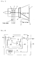
- the cathode ray tube of Figure 1 has a cathode 3 with a heater 2, a grid electrode 4 and an accelerating electrode 5. Electron beams generated at the cathode are accelerated through the tube and redirected by the deflection yoke 6 to a fluorescent body 7 to create a visible image.
- the amount of beam current in the cathode ray tube can be controlled by varying the voltage between the grid electrode and the cathode of the cathode ray tube.
- the conventional cathode ray tube operates as follows.
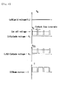
- the grid electrode is grounded and a video signal as shown in Fig. 8b (a white signal) is applied to the cathode so that a voltage V CG can be loaded between the grid electrode and the cathode, and current I can flow inverse-proportional to the voltage V CG in the cathode ray tube to control beam current.
- the intervals of high voltage depicted in narrow width in Fig. 8b are flyback line intervals, in which no current flows because the voltage is higher than the cut-off voltage (limited voltage disabling beams to flow).
- the amount of current is controlled by the conventional method as described above, same beam current flows on a video signal level of the same voltage.
- the amount of beam current arrived at the fluorescent body in the middle area of the panel is equal to that arrived at the fluorescent body around edge area of the panel.
- the brightness becomes lower around edge area than around middle area because the thickness of the panel glass is greater and the optical transmissibility is lower around edge area than in the middle area thereof.
- the amount of light generated by emitting a fluorescent body with electron beams is proportional to.the amount of electron beam current as shown in Figs. 4a to 4c.
- the light emitted from the fluorescent body reaches'human eyes through the glass.
- some amount of the light is absorbed, while the remaining amount thereof pass through the glass.
- transmissibility of the glass is variable depending on thickness of the glass, as shown in Fig. 4b. As the glass becomes thicker, the amount of light passing through the glass becomes lesser.
- the present invention employs a mechanism such that less amount of beam current arrives at the fluorescent body of the thin glass, as shown in Fig. 6a, and more amount of beam current arrives at the fluorescent body of the thick glass.
- the amount of light emitted from the fluorescent body becomes relatively greater in the thick glass than in the thin glass, thereby equalizing the amount of light passing through the thick glass with that passing through the thin glass even if the thick glass has lower transmissibility.
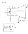
- the present invention additionally provides a brightness compensating circuit 11 to the electron gun 10 of the cathode ray tube for controlling the electron beam current so as to correct the difference in brightness variable in accordance with the thickness difference in the glass of the panel in the grid electrode 4, which is one of the terminals for controlling the amount of beam current.
- the present invention inputs in the grid electrode 4 a voltage waveform for compensating brightness to control the current instead of grounding the voltage 0V around the grid electrode 4 of the conventional cathode ray tube as shown in Fig. 1.
- the present invention does not apply a static voltage (0V in general) to the grid electrode of the cathode ray tube, unlike the conventional method. Rather, the present invention applies a voltage, which has a waveform calculated in accordance with the transmissibility as shown in Fig. 9a, so as to be low in the middle area and high around edge area, thereby resulting in the waveform of the electric potential difference (electric potential difference between the grid electrode and the cathode" V CG ) from the video signal [V c in Fig. 9b] loaded on the cathode to be as shown in Fig. 9c.
- the brightness compensating voltage is applied to the grid electrode by the brightness compensating circuit 11 as shown in Fig. 7.
- Vertical and horizontal parabolic voltages are inputted in the brightness compensating circuit 11, as in case of a dynamic focus circuit of the conventional cathode ray tube.
- the parabola input voltage is applied to the grid electrode 4 through an amplifying terminal, which comprises a transistor Q1 and resistors R1, R2.
- the thickness around the middle area is set to be ranged 12.5-14.5mm and the thickness around the edge area is set to be ranged 25.5-29.6mm so as to have a wedge ratio of about 204% in the glass for a cathode ray tube generally known to be the clear glass, the brightness difference between the middle area and the edge area becomes 6.6% if the same level of beam current is used in those portions.
- the brightness difference becomes 23.2% if the same level of beam current is used in the middle area and the edge area of the screen glass.
- the thickness of the middle area is set to be ranged 12.5-14.5mm and the thickness of the edge area is set to be ranged 25.5-29.6mm in the flat glass for a cathode ray tube generally known to be the dark tint glass so as to have a wedge ratio of about 204%, the brightness difference becomes 22.4% if the same level of beam current is used in the middle area and the edge area of the screen glass.
- the wedge ratio may be set to be greater and the beam current control range may be set to be greater than the aforementioned values if the curve ratio is set to be smaller than the aforementioned value for the purpose of improving howling characteristics and doming characteristics of a shadow mask.
- the beam current control range is limited to be about 50% and 70% in case of a cathode ray tube for TV and monitors, respectively, it is possible to obtain the above characteristics economically without taking any particular measures for focus control in the electron gun.
- the panel employed in the flat-type cathode ray tube is shaped to have an almost flat outer face and an inner face of a predetermined curve ratio.
- the ratio between the middle area and edge area of the panel is ranged about 170-230%.
- the tint glass or the dark tint glass is mainly used in a cathode ray tube of high quality to enhance contrast.
- the thickness of B is 1.7d B .
- T B (1-R) 2 *e -k(1.7dA) ⁇ (1-R) 2 *e -k(2.3dA) .
- L B should have the following value: L A x e 0.00578 x 0.7 x (12.5 ⁇ 14.5) ⁇ L B ⁇ L A x e 0.00578 x 1.3 x (12.5 ⁇ 14.5) ⁇ (1.052 ⁇ 1.060) L A ⁇ L B ⁇ (1.098 ⁇ 1.115)L A
- L B should have the following value: L A x e 0.04626 x 0.7x (12.5 ⁇ 14.5) ⁇ L B ⁇ L A x e 0.04626 x 1.3 x (12.5 ⁇ 14.5) ⁇ (1.499 ⁇ 1.599)L A ⁇ L B ⁇ (2.121 ⁇ 2.392) L A Further, assuming that the absorbancy index k of the dark tint glass is 0.06837, the thickness d A of area A is ranged 12.5-14.5mm, L B should have the following value: L A x e 0.06737 x 0.7 x (12.5 ⁇ 14.5) ⁇ L B ⁇ L A x e 0.06737 x 1.3 x (12.5 ⁇ 14.5) ⁇ (1.803 ⁇ 1.981) L A ⁇ L B ⁇ (2.988 ⁇ 3.561) L A
- the brightness of the fluorescent body is proportional to the beam current. Therefore, assuming that the thickness of area A is 12.5mm, the brightness becomes comprehensively equal if voltage is applied to the grid electrode 4 so as to flow 1.052 ⁇ 1.098 times more the beam current I A of area A to the beam current I B of B in case of the clear glass; 1.499 ⁇ 2.121 times more the beam current I A of area A to the beam current I B of B in case of the tint glass, 1.803 ⁇ 2.988 times more the beam current I A of area A to the beam current I B of B in case of the dark tint glass in accordance with their respective wedge ratios.
- the brightness becomes comprehensively equal if voltage is applied to the grid electrode 4 so as to supply 1.060 ⁇ 1.115 times more the beam current I A of area A to the beam current I B of B in case of the clear glass; 1.599 ⁇ 2.392 times more the beam current I A of area A to the beam current I B of B in case of the tint glass; and 1.981 ⁇ 3.561 times more the beam current I A of area A to the beam current I B of B in case of the dark tint glass in accordance with their respective wedge ratios.
- the difference between the aforementioned voltage and the signal voltage is the voltage of a correcting waveform around edge area of the parabolic voltage.
- the voltage V V of the correcting waveform around edge area of the parabolic voltage is a voltage to be applied to the grid electrode 4 so as to display B when the signal level is white.
- vertical and horizontal parabolic voltages of the dynamic focus circuit are inputted in the grid electrode 4 of the brightness compensating device 11 as shown in 7, as in case of the conventional cathode ray tube.
- the parabola input voltage is applied to the grid electrode 4 through the amplifying terminal, which comprises the transistor Q1 and the resistors R1, R2.
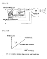
- Fig. 11 is a diagram illustrating a brightness compensating device according to another embodiment of the present invention. Referring to Fig.
- the brightness compensating device comprises a voltage control section for receiving vertical and horizontal parabolic voltages inputted in the dynamic focus circuit of the cathode ray tube operating circuit, a first amplifying section Q1 for receiving voltage in accordance with the beam current and inputting the amplified voltage in a control voltage of the voltage control section, and a second amplifying section Q2 for amplifying the vertical and horizontal parabolic voltages controlled in accordance with the output voltage of the first amplifying section Q1 so as to be applied to the grid electrode 4 of the electron gun.
- the voltage control section comprises a volume control IC.
- the vertical and horizontal parabolic voltages are inputted in the voltage control section through resistors R1 and R2, respectively.
- the first and the second amplifying sections comprise transistors Q1 and Q2, respectively.
- the parabolic voltages in which vertical and horizontal cycles are mixed, connect to the resistors R1 and R2 the vertical and the horizontal voltages amounting to tens of volts at the front terminal of a second depositor in a circuit generating the dynamic focus voltage.
- the resistors R1 and R2 divide the voltages to control volume of the waveform of the vertical and the horizontal parabolic voltages.
- the divided voltages are inputted in the volume control IC, and voltages at an ABL terminal is connected by means of the volume control IC so as to sense variation of the voltage in accordance with the beam current.
- the voltages of the ABL terminal is amplified with polarities reversed by the first amplifying section (the transistor Q1), and inputted in the control voltage of the volume control IC.
- the output of the volume control IC has different amplified ratios in accordance with the volume of the control voltage. Thus, the volume becomes greater where there is more beam current, while the volume becomes smaller where there is less beam current.
- the voltage of the volume control IC which is very small in its volume, is amplified by the second amplifying section (the transistor Q2) and inputted in the grid electrode of the electron gun.
- the ABL terminal senses the amount of beam current emitted by the cathode, and controls the parabolic voltage inputted in the grid electrode 4 of the electron gun in accordance with the sensed value so as to prevent excessive or deficient compensation for brightness.
- Cathode ray tubes having a screen of almost flat outer face were recently launched.
- the screen has a curve ratio difference between an inner face and an outer face thereof. This results in the thickness difference between the middle area and the edge area of the screen. This is generally referred to as a wedge ratio.
- the wedge ratio is ranged between 170% at the minimum and 230% at the maximum.
- Clear glass of high transmissibility is used for manufacturing a panel for screen to overcome the brightness difference caused by the thickness difference.
- the clear glass also has a transmissibility higher than 75%. Therefore, to differentiate the brightness.
- the compensating degrees in accordance with variance of the beam current by using the voltage at the ABL terminal. Then, the brightness can be maintained in a uniform or constant ratio between the middle area and the edge area of the screen regardless of the brightness level of the screen.
Landscapes
- Cathode-Ray Tubes And Fluorescent Screens For Display (AREA)
- Video Image Reproduction Devices For Color Tv Systems (AREA)
- Details Of Television Scanning (AREA)
- Television Receiver Circuits (AREA)
- Vessels, Lead-In Wires, Accessory Apparatuses For Cathode-Ray Tubes (AREA)
- Transforming Electric Information Into Light Information (AREA)
Applications Claiming Priority (4)
| Application Number | Priority Date | Filing Date | Title |
|---|---|---|---|
| KR2002026921 | 2002-05-15 | ||
| KR20020026921 | 2002-05-15 | ||
| KR2002032245 | 2002-06-10 | ||
| KR10-2002-0032245A KR100474331B1 (ko) | 2002-05-15 | 2002-06-10 | 컬러 화상표시장치 |
Publications (2)
| Publication Number | Publication Date |
|---|---|
| EP1363312A2 true EP1363312A2 (de) | 2003-11-19 |
| EP1363312A3 EP1363312A3 (de) | 2006-03-08 |
Family
ID=29272442
Family Applications (1)
| Application Number | Title | Priority Date | Filing Date |
|---|---|---|---|
| EP03253043A Withdrawn EP1363312A3 (de) | 2002-05-15 | 2003-05-15 | Farbbildanzeigegerät |
Country Status (4)
| Country | Link |
|---|---|
| US (1) | US6798155B2 (de) |
| EP (1) | EP1363312A3 (de) |
| JP (1) | JP2003330402A (de) |
| CN (1) | CN1458661A (de) |
Families Citing this family (2)
| Publication number | Priority date | Publication date | Assignee | Title |
|---|---|---|---|---|
| JP2003304558A (ja) * | 2002-04-09 | 2003-10-24 | Sanyo Electric Co Ltd | ブルーストレッチ回路及びレベル検出回路 |
| CN103376343B (zh) * | 2012-04-28 | 2015-11-04 | 中国科学院电子学研究所 | 一种用于强流电子注分析仪的可移动极间距电子枪系统 |
Family Cites Families (16)
| Publication number | Priority date | Publication date | Assignee | Title |
|---|---|---|---|---|
| DE2030384A1 (de) * | 1969-06-30 | 1971-01-14 | Sony Corp Tokio | Kathodenstrahlrohre |
| US4319163A (en) * | 1980-06-30 | 1982-03-09 | Rca Corporation | Electron gun with deflection-synchronized astigmatic screen grid means |
| JPS63237334A (ja) * | 1987-03-25 | 1988-10-03 | Iwatsu Electric Co Ltd | 電子管の電子銃 |
| DE3721326A1 (de) * | 1987-06-27 | 1989-01-12 | Triumph Adler Ag | Ansteuerverfahren fuer eine bildroehre mit unterschiedlich dicker frontscheibe und schaltungsanordnung zur durchfuehrung des verfahrens |
| US4916365A (en) * | 1987-08-31 | 1990-04-10 | Anritsu Corporation | Color CRT displaying correction circuit |
| JPH03205966A (ja) * | 1988-10-18 | 1991-09-09 | Samsung Electron Devices Co Ltd | 輝度補生回路 |
| JPH087537B2 (ja) * | 1989-06-23 | 1996-01-29 | アンリツ株式会社 | Crt表示装置の輝度むら補正回路 |
| US5077502A (en) | 1990-04-26 | 1991-12-31 | Honeywell Inc. | Compensation for drift in a cathode ray tube |
| JP3510339B2 (ja) * | 1994-08-01 | 2004-03-29 | 株式会社 日立ディスプレイズ | カラー陰極線管 |
| TW272299B (de) * | 1994-08-01 | 1996-03-11 | Toshiba Co Ltd | |
| JPH08298080A (ja) * | 1995-04-27 | 1996-11-12 | Nec Kansai Ltd | 電子銃 |
| JPH08336062A (ja) * | 1995-06-08 | 1996-12-17 | Sony Corp | テレビジョン受像機 |
| KR100258982B1 (ko) | 1997-12-02 | 2000-06-15 | 윤종용 | 모니터의 화면 휘도 조정부 |
| JP2000125225A (ja) | 1998-10-15 | 2000-04-28 | Matsushita Electric Ind Co Ltd | 輝度補正装置 |
| KR100298408B1 (ko) * | 1998-11-18 | 2001-08-07 | 구자홍 | 음극선관의코너포커스및휘도보정장치 |
| JP2002042698A (ja) * | 2000-07-27 | 2002-02-08 | Hitachi Ltd | パネル表面がフラットなシャドーマスク型カラー陰極線管 |
-
2002
- 2002-09-17 US US10/244,739 patent/US6798155B2/en not_active Expired - Fee Related
- 2002-10-16 CN CN02131485A patent/CN1458661A/zh active Pending
- 2002-10-30 JP JP2002315465A patent/JP2003330402A/ja active Pending
-
2003
- 2003-05-15 EP EP03253043A patent/EP1363312A3/de not_active Withdrawn
Non-Patent Citations (1)
| Title |
|---|
| None * |
Also Published As
| Publication number | Publication date |
|---|---|
| EP1363312A3 (de) | 2006-03-08 |
| US20030214261A1 (en) | 2003-11-20 |
| US6798155B2 (en) | 2004-09-28 |
| CN1458661A (zh) | 2003-11-26 |
| JP2003330402A (ja) | 2003-11-19 |
Similar Documents
| Publication | Publication Date | Title |
|---|---|---|
| US4205252A (en) | Flat cathode ray tube with repeller electrode | |
| EP1363312A2 (de) | Farbbildanzeigegerät | |
| GB2049989A (en) | Cathode ray tube having low voltage focus and dynamic correction | |
| US6034742A (en) | Adaptive sharpness enhancement for a multi-frequency scanning monitor | |
| US6259484B1 (en) | Method and apparatus for centering a video signal on a display screen | |
| US6348944B1 (en) | Selective aging for monitor production | |
| KR100474331B1 (ko) | 컬러 화상표시장치 | |
| US6420841B2 (en) | Color display device | |
| JP2748901B2 (ja) | 冷陰極駆動回路およびこれを用いた電子ビーム装置 | |
| US5977711A (en) | Method and system for optimizing cathode output for aging a cathode ray tube during manufacture | |
| US6605898B2 (en) | CRT device with improved resolution | |
| KR19980701605A (ko) | 음극선 튜브로 구성된 디스플레이 시스템과 디스플레이 시스템에 신호를 전송하는 수단을 포함하는 컴퓨터 | |
| KR100440526B1 (ko) | Crt 표시 장치 | |
| US20040140751A1 (en) | Display tube and display device | |
| JP3125598B2 (ja) | 平板型画像表示装置 | |
| JP2866721B2 (ja) | 陰極線管駆動装置 | |
| JP2002099233A (ja) | 陰極線管およびその輝度変動抑制回路 | |
| JP2000032484A (ja) | 画像表示装置 | |
| KR19990080539A (ko) | 모니터의 래스터 안정화회로 | |
| JPH06261219A (ja) | ディスプレイモニタ | |
| JPH07201292A (ja) | Crtディスプレイの鮮鋭度改善回路 | |
| JPH02139836A (ja) | 平板型画像表示装置 | |
| JPH11233043A (ja) | 電子銃装置および陰極線管装置 | |
| JPH07169418A (ja) | 平板型画像表示装置 | |
| JPH10215463A (ja) | 自動白バランス調整回路を有するカラー受像管を用いたディスプレイ |
Legal Events
| Date | Code | Title | Description |
|---|---|---|---|
| PUAI | Public reference made under article 153(3) epc to a published international application that has entered the european phase |
Free format text: ORIGINAL CODE: 0009012 |
|
| AK | Designated contracting states |
Kind code of ref document: A2 Designated state(s): AT BE BG CH CY CZ DE DK EE ES FI FR GB GR HU IE IT LI LU MC NL PT RO SE SI SK TR |
|
| AX | Request for extension of the european patent |
Extension state: AL LT LV MK |
|
| RIN1 | Information on inventor provided before grant (corrected) |
Inventor name: LIM, JONG-HO Inventor name: HEO, MAN-HO Inventor name: KIM, JI-HYUN |
|
| RIC1 | Information provided on ipc code assigned before grant |
Ipc: 7H 04N 5/68 B Ipc: 7H 04N 5/57 A |
|
| PUAL | Search report despatched |
Free format text: ORIGINAL CODE: 0009013 |
|
| AK | Designated contracting states |
Kind code of ref document: A3 Designated state(s): AT BE BG CH CY CZ DE DK EE ES FI FR GB GR HU IE IT LI LU MC NL PT RO SE SI SK TR |
|
| AX | Request for extension of the european patent |
Extension state: AL LT LV MK |
|
| RIC1 | Information provided on ipc code assigned before grant |
Ipc: H04N 5/20 20060101ALI20060117BHEP Ipc: H01J 29/52 20060101ALI20060117BHEP Ipc: H04N 5/68 20060101ALI20060117BHEP Ipc: H04N 5/57 20060101AFI20050411BHEP |
|
| 17P | Request for examination filed |
Effective date: 20060908 |
|
| AKX | Designation fees paid |
Designated state(s): NL |
|
| 17Q | First examination report despatched |
Effective date: 20061115 |
|
| REG | Reference to a national code |
Ref country code: DE Ref legal event code: 8566 |
|
| RIN1 | Information on inventor provided before grant (corrected) |
Inventor name: LIM, JONG-HO Inventor name: HEO, MAN-HO Inventor name: KIM, JI-HYUN |
|
| STAA | Information on the status of an ep patent application or granted ep patent |
Free format text: STATUS: THE APPLICATION IS DEEMED TO BE WITHDRAWN |
|
| 18D | Application deemed to be withdrawn |
Effective date: 20091201 |