EP1361961B1 - Forming a mark on a gemstone or industrial diamond - Google Patents
Forming a mark on a gemstone or industrial diamond Download PDFInfo
- Publication number
- EP1361961B1 EP1361961B1 EP02711117A EP02711117A EP1361961B1 EP 1361961 B1 EP1361961 B1 EP 1361961B1 EP 02711117 A EP02711117 A EP 02711117A EP 02711117 A EP02711117 A EP 02711117A EP 1361961 B1 EP1361961 B1 EP 1361961B1
- Authority
- EP
- European Patent Office
- Prior art keywords
- setting
- exposure
- radiation
- image
- diamond
- Prior art date
- Legal status (The legal status is an assumption and is not a legal conclusion. Google has not performed a legal analysis and makes no representation as to the accuracy of the status listed.)
- Expired - Lifetime
Links
- 239000010432 diamond Substances 0.000 title claims abstract description 98
- 229910003460 diamond Inorganic materials 0.000 title claims abstract description 90
- 239000010437 gem Substances 0.000 title claims description 59
- 229910001751 gemstone Inorganic materials 0.000 title claims description 59
- 230000005855 radiation Effects 0.000 claims abstract description 106
- 229920002120 photoresistant polymer Polymers 0.000 claims abstract description 4
- 238000000034 method Methods 0.000 claims description 32
- 230000003287 optical effect Effects 0.000 claims description 16
- 230000000873 masking effect Effects 0.000 claims description 7
- 239000004973 liquid crystal related substance Substances 0.000 claims description 5
- 238000001459 lithography Methods 0.000 claims 1
- 238000010438 heat treatment Methods 0.000 abstract description 5
- 238000005286 illumination Methods 0.000 description 14
- 230000000694 effects Effects 0.000 description 7
- XKRFYHLGVUSROY-UHFFFAOYSA-N Argon Chemical compound [Ar] XKRFYHLGVUSROY-UHFFFAOYSA-N 0.000 description 6
- 238000001393 microlithography Methods 0.000 description 6
- 238000004140 cleaning Methods 0.000 description 4
- 229920001971 elastomer Polymers 0.000 description 4
- 230000009467 reduction Effects 0.000 description 4
- 238000012360 testing method Methods 0.000 description 4
- OKTJSMMVPCPJKN-UHFFFAOYSA-N Carbon Chemical compound [C] OKTJSMMVPCPJKN-UHFFFAOYSA-N 0.000 description 3
- 229910052786 argon Inorganic materials 0.000 description 3
- QVGXLLKOCUKJST-UHFFFAOYSA-N atomic oxygen Chemical compound [O] QVGXLLKOCUKJST-UHFFFAOYSA-N 0.000 description 3
- 238000011161 development Methods 0.000 description 3
- 239000000806 elastomer Substances 0.000 description 3
- 238000005530 etching Methods 0.000 description 3
- 238000003384 imaging method Methods 0.000 description 3
- 239000007788 liquid Substances 0.000 description 3
- 239000000463 material Substances 0.000 description 3
- 229910052760 oxygen Inorganic materials 0.000 description 3
- 239000001301 oxygen Substances 0.000 description 3
- 238000001020 plasma etching Methods 0.000 description 3
- 239000004575 stone Substances 0.000 description 3
- MYMOFIZGZYHOMD-UHFFFAOYSA-N Dioxygen Chemical compound O=O MYMOFIZGZYHOMD-UHFFFAOYSA-N 0.000 description 2
- 230000004075 alteration Effects 0.000 description 2
- 239000011248 coating agent Substances 0.000 description 2
- 238000000576 coating method Methods 0.000 description 2
- 230000007547 defect Effects 0.000 description 2
- 238000005516 engineering process Methods 0.000 description 2
- 229910002804 graphite Inorganic materials 0.000 description 2
- 239000010439 graphite Substances 0.000 description 2
- 229910052736 halogen Inorganic materials 0.000 description 2
- 238000002347 injection Methods 0.000 description 2
- 239000007924 injection Substances 0.000 description 2
- QSHDDOUJBYECFT-UHFFFAOYSA-N mercury Chemical compound [Hg] QSHDDOUJBYECFT-UHFFFAOYSA-N 0.000 description 2
- 229910052753 mercury Inorganic materials 0.000 description 2
- 238000003801 milling Methods 0.000 description 2
- 229910000679 solder Inorganic materials 0.000 description 2
- 229910052721 tungsten Inorganic materials 0.000 description 2
- 239000010937 tungsten Substances 0.000 description 2
- 229910052724 xenon Inorganic materials 0.000 description 2
- FHNFHKCVQCLJFQ-UHFFFAOYSA-N xenon atom Chemical compound [Xe] FHNFHKCVQCLJFQ-UHFFFAOYSA-N 0.000 description 2
- LFQSCWFLJHTTHZ-UHFFFAOYSA-N Ethanol Chemical compound CCO LFQSCWFLJHTTHZ-UHFFFAOYSA-N 0.000 description 1
- XUIMIQQOPSSXEZ-UHFFFAOYSA-N Silicon Chemical compound [Si] XUIMIQQOPSSXEZ-UHFFFAOYSA-N 0.000 description 1
- 238000000149 argon plasma sintering Methods 0.000 description 1
- 238000003491 array Methods 0.000 description 1
- 239000011324 bead Substances 0.000 description 1
- 230000003796 beauty Effects 0.000 description 1
- 230000008901 benefit Effects 0.000 description 1
- 238000005513 bias potential Methods 0.000 description 1
- 229910052799 carbon Inorganic materials 0.000 description 1
- 230000008859 change Effects 0.000 description 1
- 238000006243 chemical reaction Methods 0.000 description 1
- 238000012937 correction Methods 0.000 description 1
- 238000010586 diagram Methods 0.000 description 1
- URQUNWYOBNUYJQ-UHFFFAOYSA-N diazonaphthoquinone Chemical compound C1=CC=C2C(=O)C(=[N]=[N])C=CC2=C1 URQUNWYOBNUYJQ-UHFFFAOYSA-N 0.000 description 1
- 238000009792 diffusion process Methods 0.000 description 1
- 238000001035 drying Methods 0.000 description 1
- 230000005670 electromagnetic radiation Effects 0.000 description 1
- 239000000835 fiber Substances 0.000 description 1
- 230000014509 gene expression Effects 0.000 description 1
- 239000011521 glass Substances 0.000 description 1
- 150000002367 halogens Chemical class 0.000 description 1
- 230000001939 inductive effect Effects 0.000 description 1
- 238000001746 injection moulding Methods 0.000 description 1
- 150000002500 ions Chemical class 0.000 description 1
- 230000001678 irradiating effect Effects 0.000 description 1
- 238000004519 manufacturing process Methods 0.000 description 1
- 238000005259 measurement Methods 0.000 description 1
- 230000007246 mechanism Effects 0.000 description 1
- 229910001507 metal halide Inorganic materials 0.000 description 1
- 150000005309 metal halides Chemical class 0.000 description 1
- 239000000203 mixture Substances 0.000 description 1
- 229920003986 novolac Polymers 0.000 description 1
- 238000000059 patterning Methods 0.000 description 1
- 238000000206 photolithography Methods 0.000 description 1
- 230000008569 process Effects 0.000 description 1
- 238000012545 processing Methods 0.000 description 1
- 210000001747 pupil Anatomy 0.000 description 1
- 239000004065 semiconductor Substances 0.000 description 1
- 229910052710 silicon Inorganic materials 0.000 description 1
- 239000010703 silicon Substances 0.000 description 1
- 239000002904 solvent Substances 0.000 description 1
- WFKWXMTUELFFGS-UHFFFAOYSA-N tungsten Chemical compound [W] WFKWXMTUELFFGS-UHFFFAOYSA-N 0.000 description 1
- -1 tungsten halogen Chemical class 0.000 description 1
- 238000005491 wire drawing Methods 0.000 description 1
Images
Classifications
-
- B—PERFORMING OPERATIONS; TRANSPORTING
- B44—DECORATIVE ARTS
- B44C—PRODUCING DECORATIVE EFFECTS; MOSAICS; TARSIA WORK; PAPERHANGING
- B44C1/00—Processes, not specifically provided for elsewhere, for producing decorative surface effects
- B44C1/22—Removing surface-material, e.g. by engraving, by etching
-
- B—PERFORMING OPERATIONS; TRANSPORTING
- B44—DECORATIVE ARTS
- B44C—PRODUCING DECORATIVE EFFECTS; MOSAICS; TARSIA WORK; PAPERHANGING
- B44C1/00—Processes, not specifically provided for elsewhere, for producing decorative surface effects
-
- B—PERFORMING OPERATIONS; TRANSPORTING
- B23—MACHINE TOOLS; METAL-WORKING NOT OTHERWISE PROVIDED FOR
- B23K—SOLDERING OR UNSOLDERING; WELDING; CLADDING OR PLATING BY SOLDERING OR WELDING; CUTTING BY APPLYING HEAT LOCALLY, e.g. FLAME CUTTING; WORKING BY LASER BEAM
- B23K26/00—Working by laser beam, e.g. welding, cutting or boring
- B23K26/02—Positioning or observing the workpiece, e.g. with respect to the point of impact; Aligning, aiming or focusing the laser beam
- B23K26/03—Observing, e.g. monitoring, the workpiece
- B23K26/034—Observing the temperature of the workpiece
-
- B—PERFORMING OPERATIONS; TRANSPORTING
- B44—DECORATIVE ARTS
- B44B—MACHINES, APPARATUS OR TOOLS FOR ARTISTIC WORK, e.g. FOR SCULPTURING, GUILLOCHING, CARVING, BRANDING, INLAYING
- B44B3/00—Artist's machines or apparatus equipped with tools or work holders moving or able to be controlled substantially two- dimensionally for carving, engraving, or guilloching shallow ornamenting or markings
- B44B3/06—Accessories, e.g. tool or work holders
- B44B3/065—Work holders
-
- B—PERFORMING OPERATIONS; TRANSPORTING
- B44—DECORATIVE ARTS
- B44B—MACHINES, APPARATUS OR TOOLS FOR ARTISTIC WORK, e.g. FOR SCULPTURING, GUILLOCHING, CARVING, BRANDING, INLAYING
- B44B5/00—Machines or apparatus for embossing decorations or marks, e.g. embossing coins
- B44B5/02—Dies; Accessories
- B44B5/022—Devices for holding or supporting work
-
- C—CHEMISTRY; METALLURGY
- C04—CEMENTS; CONCRETE; ARTIFICIAL STONE; CERAMICS; REFRACTORIES
- C04B—LIME, MAGNESIA; SLAG; CEMENTS; COMPOSITIONS THEREOF, e.g. MORTARS, CONCRETE OR LIKE BUILDING MATERIALS; ARTIFICIAL STONE; CERAMICS; REFRACTORIES; TREATMENT OF NATURAL STONE
- C04B41/00—After-treatment of mortars, concrete, artificial stone or ceramics; Treatment of natural stone
- C04B41/009—After-treatment of mortars, concrete, artificial stone or ceramics; Treatment of natural stone characterised by the material treated
-
- C—CHEMISTRY; METALLURGY
- C04—CEMENTS; CONCRETE; ARTIFICIAL STONE; CERAMICS; REFRACTORIES
- C04B—LIME, MAGNESIA; SLAG; CEMENTS; COMPOSITIONS THEREOF, e.g. MORTARS, CONCRETE OR LIKE BUILDING MATERIALS; ARTIFICIAL STONE; CERAMICS; REFRACTORIES; TREATMENT OF NATURAL STONE
- C04B41/00—After-treatment of mortars, concrete, artificial stone or ceramics; Treatment of natural stone
- C04B41/53—After-treatment of mortars, concrete, artificial stone or ceramics; Treatment of natural stone involving the removal of at least part of the materials of the treated article, e.g. etching, drying of hardened concrete
- C04B41/5338—Etching
- C04B41/5346—Dry etching
-
- C—CHEMISTRY; METALLURGY
- C04—CEMENTS; CONCRETE; ARTIFICIAL STONE; CERAMICS; REFRACTORIES
- C04B—LIME, MAGNESIA; SLAG; CEMENTS; COMPOSITIONS THEREOF, e.g. MORTARS, CONCRETE OR LIKE BUILDING MATERIALS; ARTIFICIAL STONE; CERAMICS; REFRACTORIES; TREATMENT OF NATURAL STONE
- C04B41/00—After-treatment of mortars, concrete, artificial stone or ceramics; Treatment of natural stone
- C04B41/80—After-treatment of mortars, concrete, artificial stone or ceramics; Treatment of natural stone of only ceramics
- C04B41/91—After-treatment of mortars, concrete, artificial stone or ceramics; Treatment of natural stone of only ceramics involving the removal of part of the materials of the treated articles, e.g. etching
Definitions
- the use of the setting-up image provides a simple way of locating (registration) and orientating the exposure image. Furthermore, the use of the setting-up image provides a good way of focusing the exposure image, for instance when projecting the image of a mask using visible or ultraviolet light. The operator may alter the position of the gemstone or industrial diamond relative to the focal plane using mechanical adjustments. If the setting-up image is projected through an objective lens or lens system and is sensed through the objective lens or lens system, the apparent error in focus is doubled because the setting-up radiation is reflected back through the objective lens or lenses and hence travels a distance equal to twice the error in focus; this exaggeration of the focus error enables the focus to be set very accurately and easily. However, it is possible to insert say a beam splitter between the objective lens or lens system and the gemstone or diamond and sense the image without it passing through the primary objective lens or lens system.
- the setting-up image may be sensed by an electronic image detector, using any suitable wavelength for the setting-up radiation, or, if the setting-up radiation is in the visible range, the setting-up image can be viewed by eye.
- the exposure region of a mask may define a shape corresponding to that of the micro mark to be formed or may define alignment marks to assist in the accurate location of the exposure image on the stone.
- the exposure radiation is scanned, such as in the case of a laser beam, the exposure radiation can be scanned through the exposure region, carrying out direct beam writing. In theory it would be possible to have the alignment region transparent or have no mask at all and the setting-up radiation also scanned.
- the diamond 7 can now be cleaned, for instance by mechanical cleaning with swabs moistened in alcohol or by drawing the diamond 7 and dop 11 across a proprietary optical lens cleaning tissue.
- the dop 11 may be mounted on a vacuum chuck and rotated about an axis preferably perpendicular to the table 7a of the diamond 7.
- a solvent can be applied, followed by spin drying or mechanical cleaning.
- Photoresist is applied to cover at least the table 7a of the diamond 7.
- a suitable positive-tone resist material is Microposit 1818, manufactured by the Shipley Company, which is a diazonaphthoquinone/novolak resist.
- the chuck with the dop 11 and stone 7 are rotated at high speed, typically 4000 to 8000 r.p.m., for a period of typically 15 to 30 seconds. This results in a film of resist of uniform thickness over the greater part of the diamond table 7a, of typically one to two microns. If the top surface is continuous across the diamond table 7a, the surface of the setting material 2 and the tops of the sidewalls 5 of the dop 11, no bead or rim would be formed on the diamond table 7a.
- the resist is then baked. Typical conditions will be one minute at 115°C. This can be done by placing the dop 11 on a Peltier device with the culet of the diamond 7 in a pool of liquid solder contained in the device tip. Alternatively, the heating effect may be produced by a hotplate, inductive heating, a heating element incorporated in the dop 11, steam or liquid solder circulated over the culet, infra-red radiation on the table 7a. The temperature of the dop 11 may be measured by a thermocouple mounted in the dop 11 or in contact with it, and this measurement can control the heating means to regulate the temperature. Alternatively, the temperature may be measured and controlled through the Peltier device.
- the source of heat is discontinued and the dop 11 quickly cooled, e.g. using the Peltier device as a cooler.
- the diamond 7 is now ready for exposure of the resist.
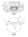
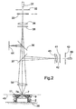
- Figure 2 shows the optical system of one arrangement for exposing the resist.
- the diamond 7 is in the dop 11 with a locating surface defined by the underside of the dop ring 2.
- the upper surface of the platen or table 30 forms an upwards-facing register surface.
- the table 7a of the diamond 7 is accurately positioned parallel to the table 30.
- the mark could be formed at the centre of the table 7a or at the edge of the table 7a.
- the dop 11 can slide across the table 30 and can thus be adjusted manually, or the position and rotation of the table 30 can be adjusted.
- the optical system has a setting-up/exposure radiation sources (or sources) 31, a setting-up/exposure aperture stop 32, an exposure shutter 33, a setting-up/exposure field lens 34, a setting-up/exposure mask 35, a first beam splitter 36, a second beam splitter 37, an objective lens 38, an illumination radiation source 39, an illumination radiation aperture stop 40, an illumination radiation filter 41, an illumination radiation field lens 42, an illumination radiation field stop 43 and an observation plane 44.
- the objective lens 38 forms an image of the mask 35 at the focal plane 45. It is desirable but not essential that the objective lens 38 has the same focal length for both setting-up and exposure wavelengths and has good aberration correction for both the setting-up and exposure radiation wavelengths.
- the exposure shutter 33 can be incorporated such that when it is closed, it provides a filter to block the exposure radiation while transmitting the setting-up radiation.
- the exposure shutter 33 can be located anywhere in the radiation path, and may be incorporated in the source 31 or in the mask 35.
- the setting-up radiation provides the setting-up image of the mask 35 on the table 7a of the diamond 7.
- the optical system substantially reduces the image size relative to the mask.
- the setting-up (and exposure) image can be reduced by about 90 per cent (x10 reduction) compared to the mask 35. In general, the reduction is preferably from about x10 to about x20 or up to about x100.
- the setting-up radiation does not affect the facet of the gemstone in such a way that a mark is formed - for instance, if photolithography is being used, the setting-up radiation must not expose the resist.
- the setting-up radiation can be green or yellow light in the wavelength range 500 to 550 nm, i.e. in the same range as the illuminating radiation. In general, if its intensity is sufficiently low, much lower than that of the exposure radiation, the setting-up radiation could be the same as the exposure radiation.
- Black lines are parts that transmit radiation.
- the edge of the table 7a is indicated with dot-dash lines.
- the "TEST 1234" feature transmits at least the exposure radiation.
- the "TEST 1234" feature is focused using a standard focusing arrangement (not shown).
- a corner of the table 7a is then placed on the line 37 and is moved manually up towards the centre of the image.
- Standard x and y direction micrometer adjustments can be provided for fine adjustment of the image in relation to the diamond table 7a. If the diamond 7 has a regular octagonal table 7a, with corner angles of 135°, the edges of the table 7a are aligned with the lines 51, 53; the setting-up image is then properly located and orientated. If the diamond does not have a 135° corner angle, the edges of the table 7a can be brought into contact with the curves 54, 55 with the corner on the line 52 or on an extension of the line 52.
Landscapes
- Chemical & Material Sciences (AREA)
- Engineering & Computer Science (AREA)
- Ceramic Engineering (AREA)
- Structural Engineering (AREA)
- Organic Chemistry (AREA)
- Materials Engineering (AREA)
- Optics & Photonics (AREA)
- Physics & Mathematics (AREA)
- Mechanical Engineering (AREA)
- Plasma & Fusion (AREA)
- Adornments (AREA)
- Crystals, And After-Treatments Of Crystals (AREA)
- Carbon And Carbon Compounds (AREA)
- Exposure And Positioning Against Photoresist Photosensitive Materials (AREA)
- Laser Beam Processing (AREA)
- Processing Of Stones Or Stones Resemblance Materials (AREA)
- Investigating Materials By The Use Of Optical Means Adapted For Particular Applications (AREA)
- Manufacturing Optical Record Carriers (AREA)
Applications Claiming Priority (3)
| Application Number | Priority Date | Filing Date | Title |
|---|---|---|---|
| GB0103881 | 2001-02-16 | ||
| GBGB0103881.9A GB0103881D0 (en) | 2001-02-16 | 2001-02-16 | E-beam marking |
| PCT/GB2002/000709 WO2002066262A2 (en) | 2001-02-16 | 2002-02-18 | Forming a mark on a gemstone or industrial diamond |
Publications (2)
| Publication Number | Publication Date |
|---|---|
| EP1361961A2 EP1361961A2 (en) | 2003-11-19 |
| EP1361961B1 true EP1361961B1 (en) | 2011-06-29 |
Family
ID=9908917
Family Applications (2)
| Application Number | Title | Priority Date | Filing Date |
|---|---|---|---|
| EP02711117A Expired - Lifetime EP1361961B1 (en) | 2001-02-16 | 2002-02-18 | Forming a mark on a gemstone or industrial diamond |
| EP02712089A Expired - Lifetime EP1365930B1 (en) | 2001-02-16 | 2002-02-18 | Method and device for mounting and preparing a gemstone or industrial diamond for the formation of a mark on the surface thereof |
Family Applications After (1)
| Application Number | Title | Priority Date | Filing Date |
|---|---|---|---|
| EP02712089A Expired - Lifetime EP1365930B1 (en) | 2001-02-16 | 2002-02-18 | Method and device for mounting and preparing a gemstone or industrial diamond for the formation of a mark on the surface thereof |
Country Status (13)
| Country | Link |
|---|---|
| EP (2) | EP1361961B1 (cg-RX-API-DMAC7.html) |
| JP (2) | JP4331941B2 (cg-RX-API-DMAC7.html) |
| KR (2) | KR100978547B1 (cg-RX-API-DMAC7.html) |
| CN (2) | CN100340419C (cg-RX-API-DMAC7.html) |
| AT (2) | ATE552123T1 (cg-RX-API-DMAC7.html) |
| AU (2) | AU2002230007C1 (cg-RX-API-DMAC7.html) |
| CA (2) | CA2442584C (cg-RX-API-DMAC7.html) |
| GB (3) | GB0103881D0 (cg-RX-API-DMAC7.html) |
| IL (3) | IL157407A0 (cg-RX-API-DMAC7.html) |
| RU (2) | RU2279840C2 (cg-RX-API-DMAC7.html) |
| TW (2) | TW590863B (cg-RX-API-DMAC7.html) |
| WO (2) | WO2002066262A2 (cg-RX-API-DMAC7.html) |
| ZA (2) | ZA200306378B (cg-RX-API-DMAC7.html) |
Families Citing this family (25)
| Publication number | Priority date | Publication date | Assignee | Title |
|---|---|---|---|---|
| DE102005039430A1 (de) * | 2005-08-18 | 2007-02-22 | Oc Oerlikon Balzers Ag | Lasermarkierung nahe der Oberfläche bei innenbearbeiteten transparenten Körpern |
| US8033136B2 (en) | 2005-12-06 | 2011-10-11 | California Institute Of Technology | Enhancing the optical characteristics of a gemstone |
| KR100816681B1 (ko) * | 2006-07-18 | 2008-03-27 | 참앤씨(주) | 평판 트리밍을 위한 인스펙션 장치 |
| US8069688B2 (en) | 2006-12-06 | 2011-12-06 | California Institute Of Technology | Gemstones and methods for controlling the appearance thereof |
| JP5435901B2 (ja) * | 2008-06-28 | 2014-03-05 | 日本写真印刷株式会社 | 宝石をインサートした樹脂成形品の製造方法 |
| AT11232U1 (de) * | 2009-03-27 | 2010-07-15 | Swarovski & Co | Schmuckstein mit verspiegelter vorderseite |
| PL2414130T5 (pl) | 2009-03-30 | 2019-10-31 | Boegli Gravures Sa | Sposób i urządzenie do strukturyzowania powierzchni obiektu litego z twardą powłoką pierwszym laserem o impulsach w zakresie nanosekundowym i drugim laserem o impulsach w zakresie piko- lub femtosekundowym; folia opakowaniowa |
| AT507883B1 (de) | 2009-05-19 | 2010-09-15 | Swarovski & Co | Spritzgegossener dekorationsartikel |
| CN102152231B (zh) * | 2011-01-28 | 2013-08-14 | 金华冠华水晶有限公司 | 将双端锥形的钻石坯固定朝向的设备 |
| RU2505386C2 (ru) * | 2011-09-28 | 2014-01-27 | ООО Научно-производственный центр "Лазеры и аппаратура ТМ" | Способ лазерной обработки материалов и устройство для его осуществления |
| US8928973B2 (en) * | 2011-12-16 | 2015-01-06 | Taiwan Semiconductor Manufacturing Company, Ltd. | Microscope apparatus for phase image acquisition |
| US10259080B1 (en) | 2013-04-26 | 2019-04-16 | Vactronix Scientific, Llc | Adaptive guide bushing for laser tube cutting systems |
| US11969819B2 (en) | 2013-04-26 | 2024-04-30 | Vactronix Scientific, Llc | Adaptive guide bushing for laser tube cutting systems |
| HK1198858A2 (en) * | 2014-04-16 | 2015-06-12 | Master Dynamic Limited | Method of marking a solid state material, and solid state materials marked according to such a method |
| KR101559935B1 (ko) * | 2015-07-31 | 2015-10-14 | 윤선용 | 사전 왜곡한 이미지를 이용하여 보석 표면에 이미지를 출력하는 장치 및 방법 |
| MX2018010237A (es) * | 2016-02-24 | 2019-01-14 | David Yurman IP LLC | Meteorito fundido. |
| CN107351591A (zh) * | 2016-05-09 | 2017-11-17 | 重庆长寿古镇文化旅游开发有限公司 | 古建筑或仿古建筑梁枋彩绘纹样线条快速放样装置和方法 |
| CN106226994A (zh) * | 2016-08-31 | 2016-12-14 | 北京埃德万斯离子束技术研究所股份有限公司 | 一种基于离子束刻蚀的打标方法及应用 |
| GB2555463A (en) * | 2016-10-31 | 2018-05-02 | De Beers Uk Ltd | Apparatus and method for applying a coating to gemstones |
| US20210146716A1 (en) * | 2018-02-23 | 2021-05-20 | Master Dynamic Limited | Method of marking a solid-state material, markings formed from such methods and solid-state materials marked according to such a method |
| RU2720100C1 (ru) * | 2019-03-26 | 2020-04-24 | Акционерная Компания "АЛРОСА" (публичное акционерное общество) (АК "АЛРОСА" (ПАО)) | Способ создания и детектирования оптически проницаемого изображения внутри алмаза и системы для детектирования (варианты) |
| CN110877494B (zh) * | 2019-12-28 | 2020-09-04 | 南京溧水高新创业投资管理有限公司 | 一种用于小型石板作画的雕刻机 |
| CN111319385A (zh) * | 2020-03-25 | 2020-06-23 | 赵国柱 | 首饰反射式投影图案的加工方法 |
| TWI814173B (zh) * | 2020-12-14 | 2023-09-01 | 香港商金展科技有限公司 | 在多個寶石的外表面形成可識別標記的方法和系統,以及根據這種方法標記的寶石 |
| WO2025074213A1 (en) * | 2023-10-03 | 2025-04-10 | Opsydia Limited | Gemstone inscription viewing system and applications thereof |
Citations (1)
| Publication number | Priority date | Publication date | Assignee | Title |
|---|---|---|---|---|
| WO1999000706A1 (en) * | 1997-06-27 | 1999-01-07 | Cooper Gregory D | Transferring a programmable pattern by photon lithography |
Family Cites Families (18)
| Publication number | Priority date | Publication date | Assignee | Title |
|---|---|---|---|---|
| US3527198A (en) * | 1966-03-26 | 1970-09-08 | Tokyo Shibaura Electric Co | Method and apparatus for working diamonds by means of laser light beam |
| SU442046A1 (ru) * | 1972-02-21 | 1974-09-05 | Предприятие П/Я Р-6495 | Устройство дл разметки драгоценных камней |
| SU491986A1 (ru) * | 1974-08-13 | 1975-11-15 | Предприятие П/Я В-2438 | Способ изготовлени магнитной головки |
| JPS5290372A (en) * | 1976-01-23 | 1977-07-29 | Okuda Kazumi | Patter embossed diamond |
| SU695760A1 (ru) * | 1976-10-26 | 1979-11-05 | Предприятие П/Я Р-6564 | Способ изготовлени штампов |
| SU837782A1 (ru) * | 1978-08-22 | 1981-06-15 | Предприятие П/Я А-1536 | Приспособление дл изготовлени устрой-CTBA КРЕплЕНи зАгОТОВОК ОпТичЕСКиХлиНз |
| US4478677A (en) * | 1983-12-22 | 1984-10-23 | International Business Machines Corporation | Laser induced dry etching of vias in glass with non-contact masking |
| US5410125A (en) * | 1990-10-11 | 1995-04-25 | Harry Winston, S.A. | Methods for producing indicia on diamonds |
| JP3104433B2 (ja) | 1992-10-16 | 2000-10-30 | 住友電気工業株式会社 | ダイヤモンドのエッチング方法 |
| DE4439714C2 (de) * | 1994-11-09 | 1997-11-06 | Fraunhofer Ges Forschung | Verfahren zum Markieren, wie Kennzeichnen und/oder Beschriften, von Produkten in einem Fertigungsablauf unter Verwendung von Laserstrahlung |
| US5760367A (en) * | 1995-05-16 | 1998-06-02 | Engraving Technologies, Inc. | Apparatus and method of engraving indicia on gemstones, and gemstones, produced thereby |
| GB9514558D0 (en) * | 1995-07-17 | 1995-09-13 | Gersan Ets | Marking diamond |
| US5932119A (en) * | 1996-01-05 | 1999-08-03 | Lazare Kaplan International, Inc. | Laser marking system |
| GB2325439A (en) | 1997-05-23 | 1998-11-25 | Gersan Ets | Marking diamond gemstone by plasma or ion beam etching through a laser ablated resist |
| IL124592A (en) * | 1997-05-23 | 2002-07-25 | Gersan Ets | Method of marking a gemstone or diamond |
| US6016185A (en) | 1997-10-23 | 2000-01-18 | Hugle Lithography | Lens array photolithography |
| EP1202776A1 (en) * | 1999-06-16 | 2002-05-08 | Norsam Technologies | Method apparatus and article of manufacture for a branding diamond branding with a focused ion beam |
| CN1264541A (zh) * | 2000-01-27 | 2000-08-30 | 李军 | 7%狼毒乌头碱白僵菌素悬浮剂及其生产方法 |
-
2001
- 2001-02-16 GB GBGB0103881.9A patent/GB0103881D0/en not_active Ceased
-
2002
- 2002-02-15 TW TW091102622A patent/TW590863B/zh not_active IP Right Cessation
- 2002-02-18 JP JP2002565802A patent/JP4331941B2/ja not_active Expired - Fee Related
- 2002-02-18 JP JP2002565801A patent/JP4386640B2/ja not_active Expired - Fee Related
- 2002-02-18 RU RU2003127842/12A patent/RU2279840C2/ru not_active IP Right Cessation
- 2002-02-18 EP EP02711117A patent/EP1361961B1/en not_active Expired - Lifetime
- 2002-02-18 AU AU2002230007A patent/AU2002230007C1/en not_active Ceased
- 2002-02-18 CA CA2442584A patent/CA2442584C/en not_active Expired - Fee Related
- 2002-02-18 AU AU2002231996A patent/AU2002231996B2/en not_active Ceased
- 2002-02-18 KR KR1020037010809A patent/KR100978547B1/ko not_active Expired - Fee Related
- 2002-02-18 RU RU2003127843/12A patent/RU2285619C2/ru not_active IP Right Cessation
- 2002-02-18 TW TW091102670A patent/TW552187B/zh not_active IP Right Cessation
- 2002-02-18 GB GB0321740A patent/GB2389070B/en not_active Expired - Fee Related
- 2002-02-18 GB GB0321739A patent/GB2389340B/en not_active Expired - Fee Related
- 2002-02-18 EP EP02712089A patent/EP1365930B1/en not_active Expired - Lifetime
- 2002-02-18 WO PCT/GB2002/000709 patent/WO2002066262A2/en not_active Ceased
- 2002-02-18 CN CNB028083148A patent/CN100340419C/zh not_active Expired - Fee Related
- 2002-02-18 AT AT02712089T patent/ATE552123T1/de active
- 2002-02-18 AT AT02711117T patent/ATE514564T1/de not_active IP Right Cessation
- 2002-02-18 IL IL15740702A patent/IL157407A0/xx active IP Right Grant
- 2002-02-18 WO PCT/GB2002/000712 patent/WO2002066263A2/en not_active Ceased
- 2002-02-18 IL IL157429A patent/IL157429A/en not_active IP Right Cessation
- 2002-02-18 CN CNB028083172A patent/CN1247387C/zh not_active Expired - Fee Related
- 2002-02-18 KR KR1020037010808A patent/KR100896783B1/ko not_active Expired - Fee Related
- 2002-02-18 CA CA002438728A patent/CA2438728C/en not_active Expired - Fee Related
-
2003
- 2003-08-14 IL IL157407A patent/IL157407A/en not_active IP Right Cessation
- 2003-08-15 ZA ZA200306378A patent/ZA200306378B/en unknown
- 2003-08-15 ZA ZA2003/06381A patent/ZA200306381B/en unknown
Patent Citations (3)
| Publication number | Priority date | Publication date | Assignee | Title |
|---|---|---|---|---|
| WO1999000706A1 (en) * | 1997-06-27 | 1999-01-07 | Cooper Gregory D | Transferring a programmable pattern by photon lithography |
| US6291110B1 (en) * | 1997-06-27 | 2001-09-18 | Pixelligent Technologies Llc | Methods for transferring a two-dimensional programmable exposure pattern for photolithography |
| US6480261B2 (en) * | 1997-06-27 | 2002-11-12 | Pixelligent Technologies Llc | Photolithographic system for exposing a wafer using a programmable mask |
Also Published As
Similar Documents
| Publication | Publication Date | Title |
|---|---|---|
| EP1361961B1 (en) | Forming a mark on a gemstone or industrial diamond | |
| AU2002230007A1 (en) | Forming a mark on a gemstone or industrial diamond | |
| TWI326015B (en) | Optical position assessment apparatus and method | |
| US4473293A (en) | Step-and-repeat projection alignment and exposure system | |
| US4573791A (en) | Step-and-repeat projection alignment and exposure system | |
| TW569304B (en) | Focusing method, position measuring method, exposure method, device manufacturing method and exposure apparatus | |
| TWI722389B (zh) | 圖案形成裝置、對齊標記檢測方法和圖案形成方法 | |
| JP2004523794A5 (cg-RX-API-DMAC7.html) | ||
| EP0017759B1 (en) | Improved step-and-repeat projection alignment and exposure system | |
| JPS5918950A (ja) | 加工片上へのマスクの投影転写装置およびその調整方法 | |
| US4577957A (en) | Bore-sighted step-and-repeat projection alignment and exposure system | |
| JP3211810B2 (ja) | 露光装置、露光方法、及び集積回路の製造方法 | |
| USH1463H (en) | Method for detecting positions of photomask and substrate | |
| JPS5974625A (ja) | 投影型露光装置 | |
| JPH09275058A (ja) | 投影露光方法 | |
| JPS62181430A (ja) | 露光装置の校正方法 | |
| JP3149869B2 (ja) | 露光装置及び露光方法 | |
| JPS6037615B2 (ja) | 投影露光装置のピント合せ方法 | |
| JP2021056479A (ja) | 立体面投影露光装置 | |
| JPH03211811A (ja) | 露光装置 |
Legal Events
| Date | Code | Title | Description |
|---|---|---|---|
| PUAI | Public reference made under article 153(3) epc to a published international application that has entered the european phase |
Free format text: ORIGINAL CODE: 0009012 |
|
| 17P | Request for examination filed |
Effective date: 20030916 |
|
| AK | Designated contracting states |
Kind code of ref document: A2 Designated state(s): AT BE CH CY DE DK ES FI FR GB GR IE IT LI LU MC NL PT SE TR |
|
| AX | Request for extension of the european patent |
Extension state: AL LT LV MK RO SI |
|
| REG | Reference to a national code |
Ref country code: HK Ref legal event code: DE Ref document number: 1060099 Country of ref document: HK |
|
| 17Q | First examination report despatched |
Effective date: 20080214 |
|
| GRAP | Despatch of communication of intention to grant a patent |
Free format text: ORIGINAL CODE: EPIDOSNIGR1 |
|
| GRAS | Grant fee paid |
Free format text: ORIGINAL CODE: EPIDOSNIGR3 |
|
| RBV | Designated contracting states (corrected) |
Designated state(s): AT BE CH CY DE DK ES FI FR GR IE IT LI LU MC NL PT SE TR |
|
| RAP1 | Party data changed (applicant data changed or rights of an application transferred) |
Owner name: DE BEERS CENTENARY AG |
|
| GRAA | (expected) grant |
Free format text: ORIGINAL CODE: 0009210 |
|
| REG | Reference to a national code |
Ref country code: DE Ref legal event code: R081 Ref document number: 60240386 Country of ref document: DE Owner name: DE BEERS UK LTD., GB Free format text: FORMER OWNER: GERSAN ESTABLISHMENT, VADUZ, LI |
|
| AK | Designated contracting states |
Kind code of ref document: B1 Designated state(s): AT BE CH CY DE DK ES FI FR GR IE IT LI LU MC NL PT SE TR |
|
| REG | Reference to a national code |
Ref country code: CH Ref legal event code: EP |
|
| REG | Reference to a national code |
Ref country code: IE Ref legal event code: FG4D |
|
| REG | Reference to a national code |
Ref country code: DE Ref legal event code: R096 Ref document number: 60240386 Country of ref document: DE Effective date: 20110818 |
|
| REG | Reference to a national code |
Ref country code: NL Ref legal event code: T3 |
|
| PG25 | Lapsed in a contracting state [announced via postgrant information from national office to epo] |
Ref country code: SE Free format text: LAPSE BECAUSE OF FAILURE TO SUBMIT A TRANSLATION OF THE DESCRIPTION OR TO PAY THE FEE WITHIN THE PRESCRIBED TIME-LIMIT Effective date: 20110629 |
|
| PG25 | Lapsed in a contracting state [announced via postgrant information from national office to epo] |
Ref country code: FI Free format text: LAPSE BECAUSE OF FAILURE TO SUBMIT A TRANSLATION OF THE DESCRIPTION OR TO PAY THE FEE WITHIN THE PRESCRIBED TIME-LIMIT Effective date: 20110629 Ref country code: AT Free format text: LAPSE BECAUSE OF FAILURE TO SUBMIT A TRANSLATION OF THE DESCRIPTION OR TO PAY THE FEE WITHIN THE PRESCRIBED TIME-LIMIT Effective date: 20110629 Ref country code: GR Free format text: LAPSE BECAUSE OF FAILURE TO SUBMIT A TRANSLATION OF THE DESCRIPTION OR TO PAY THE FEE WITHIN THE PRESCRIBED TIME-LIMIT Effective date: 20110930 |
|
| PG25 | Lapsed in a contracting state [announced via postgrant information from national office to epo] |
Ref country code: PT Free format text: LAPSE BECAUSE OF FAILURE TO SUBMIT A TRANSLATION OF THE DESCRIPTION OR TO PAY THE FEE WITHIN THE PRESCRIBED TIME-LIMIT Effective date: 20111031 |
|
| PG25 | Lapsed in a contracting state [announced via postgrant information from national office to epo] |
Ref country code: CY Free format text: LAPSE BECAUSE OF FAILURE TO SUBMIT A TRANSLATION OF THE DESCRIPTION OR TO PAY THE FEE WITHIN THE PRESCRIBED TIME-LIMIT Effective date: 20110629 |
|
| PLBE | No opposition filed within time limit |
Free format text: ORIGINAL CODE: 0009261 |
|
| STAA | Information on the status of an ep patent application or granted ep patent |
Free format text: STATUS: NO OPPOSITION FILED WITHIN TIME LIMIT |
|
| 26N | No opposition filed |
Effective date: 20120330 |
|
| PG25 | Lapsed in a contracting state [announced via postgrant information from national office to epo] |
Ref country code: DK Free format text: LAPSE BECAUSE OF FAILURE TO SUBMIT A TRANSLATION OF THE DESCRIPTION OR TO PAY THE FEE WITHIN THE PRESCRIBED TIME-LIMIT Effective date: 20110629 |
|
| REG | Reference to a national code |
Ref country code: CH Ref legal event code: NV Representative=s name: SERVOPATENT GMBH |
|
| REG | Reference to a national code |
Ref country code: DE Ref legal event code: R097 Ref document number: 60240386 Country of ref document: DE Effective date: 20120330 |
|
| PG25 | Lapsed in a contracting state [announced via postgrant information from national office to epo] |
Ref country code: MC Free format text: LAPSE BECAUSE OF NON-PAYMENT OF DUE FEES Effective date: 20120229 |
|
| REG | Reference to a national code |
Ref country code: HK Ref legal event code: WD Ref document number: 1060099 Country of ref document: HK |
|
| REG | Reference to a national code |
Ref country code: IE Ref legal event code: MM4A |
|
| PG25 | Lapsed in a contracting state [announced via postgrant information from national office to epo] |
Ref country code: IE Free format text: LAPSE BECAUSE OF NON-PAYMENT OF DUE FEES Effective date: 20120218 |
|
| PG25 | Lapsed in a contracting state [announced via postgrant information from national office to epo] |
Ref country code: ES Free format text: LAPSE BECAUSE OF FAILURE TO SUBMIT A TRANSLATION OF THE DESCRIPTION OR TO PAY THE FEE WITHIN THE PRESCRIBED TIME-LIMIT Effective date: 20111010 |
|
| PG25 | Lapsed in a contracting state [announced via postgrant information from national office to epo] |
Ref country code: TR Free format text: LAPSE BECAUSE OF FAILURE TO SUBMIT A TRANSLATION OF THE DESCRIPTION OR TO PAY THE FEE WITHIN THE PRESCRIBED TIME-LIMIT Effective date: 20110629 |
|
| PG25 | Lapsed in a contracting state [announced via postgrant information from national office to epo] |
Ref country code: LU Free format text: LAPSE BECAUSE OF NON-PAYMENT OF DUE FEES Effective date: 20120218 |
|
| REG | Reference to a national code |
Ref country code: FR Ref legal event code: PLFP Year of fee payment: 15 |
|
| REG | Reference to a national code |
Ref country code: DE Ref legal event code: R082 Ref document number: 60240386 Country of ref document: DE Representative=s name: MARKS & CLERK (LUXEMBOURG) LLP, LU Ref country code: DE Ref legal event code: R081 Ref document number: 60240386 Country of ref document: DE Owner name: DE BEERS UK LTD., GB Free format text: FORMER OWNER: DE BEERS CENTENARY AG, LUZERN, CH |
|
| REG | Reference to a national code |
Ref country code: CH Ref legal event code: NV Representative=s name: MARKS AND CLERK (LUXEMBOURG) LLP, CH Ref country code: CH Ref legal event code: PCOW Free format text: NEW ADDRESS: SEEHOFSTRASSE 9, 60004 LUZERN 6 (CH) Ref country code: CH Ref legal event code: PUE Owner name: DE BEERS UK LTD, GB Free format text: FORMER OWNER: DE BEERS CENTENARY AG, CH |
|
| REG | Reference to a national code |
Ref country code: NL Ref legal event code: PD Owner name: DE BEERS UK LTD; GB Free format text: DETAILS ASSIGNMENT: VERANDERING VAN EIGENAAR(S), OVERDRACHT; FORMER OWNER NAME: DE BEERS CENTENARY AG Effective date: 20160907 |
|
| REG | Reference to a national code |
Ref country code: FR Ref legal event code: PLFP Year of fee payment: 16 |
|
| REG | Reference to a national code |
Ref country code: FR Ref legal event code: CA Effective date: 20171030 Ref country code: FR Ref legal event code: TP Owner name: DE BEERS UK LTD, GB Effective date: 20171030 |
|
| REG | Reference to a national code |
Ref country code: FR Ref legal event code: PLFP Year of fee payment: 17 |
|
| PGFP | Annual fee paid to national office [announced via postgrant information from national office to epo] |
Ref country code: NL Payment date: 20190214 Year of fee payment: 18 |
|
| PGFP | Annual fee paid to national office [announced via postgrant information from national office to epo] |
Ref country code: CH Payment date: 20190215 Year of fee payment: 18 Ref country code: FR Payment date: 20190125 Year of fee payment: 18 Ref country code: IT Payment date: 20190221 Year of fee payment: 18 Ref country code: DE Payment date: 20190205 Year of fee payment: 18 |
|
| PGFP | Annual fee paid to national office [announced via postgrant information from national office to epo] |
Ref country code: BE Payment date: 20190124 Year of fee payment: 18 |
|
| REG | Reference to a national code |
Ref country code: DE Ref legal event code: R119 Ref document number: 60240386 Country of ref document: DE |
|
| REG | Reference to a national code |
Ref country code: CH Ref legal event code: PL |
|
| REG | Reference to a national code |
Ref country code: NL Ref legal event code: MM Effective date: 20200301 |
|
| REG | Reference to a national code |
Ref country code: BE Ref legal event code: MM Effective date: 20200229 |
|
| PG25 | Lapsed in a contracting state [announced via postgrant information from national office to epo] |
Ref country code: LI Free format text: LAPSE BECAUSE OF NON-PAYMENT OF DUE FEES Effective date: 20200229 Ref country code: CH Free format text: LAPSE BECAUSE OF NON-PAYMENT OF DUE FEES Effective date: 20200229 |
|
| PG25 | Lapsed in a contracting state [announced via postgrant information from national office to epo] |
Ref country code: NL Free format text: LAPSE BECAUSE OF NON-PAYMENT OF DUE FEES Effective date: 20200301 |
|
| PG25 | Lapsed in a contracting state [announced via postgrant information from national office to epo] |
Ref country code: DE Free format text: LAPSE BECAUSE OF NON-PAYMENT OF DUE FEES Effective date: 20200901 Ref country code: FR Free format text: LAPSE BECAUSE OF NON-PAYMENT OF DUE FEES Effective date: 20200229 |
|
| PG25 | Lapsed in a contracting state [announced via postgrant information from national office to epo] |
Ref country code: BE Free format text: LAPSE BECAUSE OF NON-PAYMENT OF DUE FEES Effective date: 20200229 |
|
| PG25 | Lapsed in a contracting state [announced via postgrant information from national office to epo] |
Ref country code: IT Free format text: LAPSE BECAUSE OF NON-PAYMENT OF DUE FEES Effective date: 20200218 |