EP1361602A2 - Verfahren zur Formgebung eines Randbereichs eines Wafers - Google Patents
Verfahren zur Formgebung eines Randbereichs eines Wafers Download PDFInfo
- Publication number
- EP1361602A2 EP1361602A2 EP03009260A EP03009260A EP1361602A2 EP 1361602 A2 EP1361602 A2 EP 1361602A2 EP 03009260 A EP03009260 A EP 03009260A EP 03009260 A EP03009260 A EP 03009260A EP 1361602 A2 EP1361602 A2 EP 1361602A2
- Authority
- EP
- European Patent Office
- Prior art keywords
- wafer
- edge
- der
- wird
- layer
- Prior art date
- Legal status (The legal status is an assumption and is not a legal conclusion. Google has not performed a legal analysis and makes no representation as to the accuracy of the status listed.)
- Withdrawn
Links
Images


Classifications
-
- H—ELECTRICITY
- H10—SEMICONDUCTOR DEVICES; ELECTRIC SOLID-STATE DEVICES NOT OTHERWISE PROVIDED FOR
- H10P—GENERIC PROCESSES OR APPARATUS FOR THE MANUFACTURE OR TREATMENT OF DEVICES COVERED BY CLASS H10
- H10P90/00—Preparation of wafers not covered by a single main group of this subclass, e.g. wafer reinforcement
- H10P90/12—Preparing bulk and homogeneous wafers
- H10P90/128—Preparing bulk and homogeneous wafers by edge treatment, e.g. chamfering
-
- B—PERFORMING OPERATIONS; TRANSPORTING
- B24—GRINDING; POLISHING
- B24B—MACHINES, DEVICES, OR PROCESSES FOR GRINDING OR POLISHING; DRESSING OR CONDITIONING OF ABRADING SURFACES; FEEDING OF GRINDING, POLISHING, OR LAPPING AGENTS
- B24B9/00—Machines or devices designed for grinding edges or bevels on work or for removing burrs; Accessories therefor
- B24B9/02—Machines or devices designed for grinding edges or bevels on work or for removing burrs; Accessories therefor characterised by a special design with respect to properties of materials specific to articles to be ground
- B24B9/06—Machines or devices designed for grinding edges or bevels on work or for removing burrs; Accessories therefor characterised by a special design with respect to properties of materials specific to articles to be ground of non-metallic inorganic material, e.g. stone, ceramics, porcelain
- B24B9/065—Machines or devices designed for grinding edges or bevels on work or for removing burrs; Accessories therefor characterised by a special design with respect to properties of materials specific to articles to be ground of non-metallic inorganic material, e.g. stone, ceramics, porcelain of thin, brittle parts, e.g. semiconductors, wafers
Definitions
- the invention relates to a method for shaping a Edge area of a wafer.
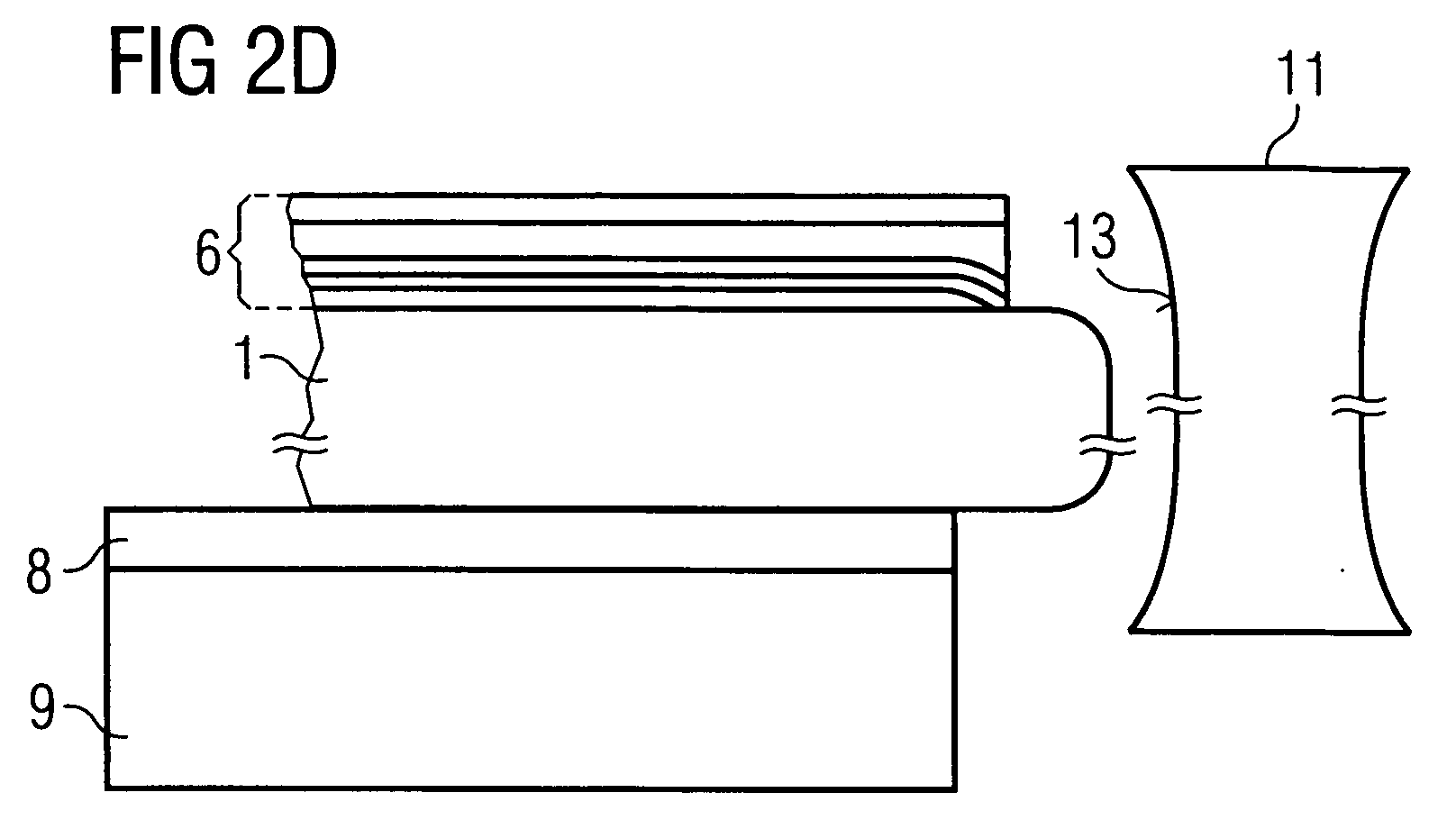
- Figure 1 (a) shows a wafer 1, on the surface 2 one A large number of layers 6 are applied.
- the wafer 1 is attached to a chuck 9 via a film 8.
- the one on the Surface 2 applied layers 6, however, cover the Wafer 1 is not complete, rather the wafer 1 is in the edge region 7 uncovered. These uncovered edge areas 7 are also necessary to avoid manufacturing problems.
- the wafer 1 has edge stripping, i.e. points in the immediate edge region 7 at the wafer edge the wafer 1 has no photoresist.
- Edge stripping i.e. points in the immediate edge region 7 at the wafer edge the wafer 1 has no photoresist.
- Edge removal or often also called “edge exclusion” is one in semiconductor technology common term and defines the unusable Area on the edge of a wafer caused by irregularities of the layers applied to the wafer or by stripping itself comes about. This edge finish is required thus the one required for the structuring Photoresist does not get onto the back 3 of the wafer 1.
- a hot disk Hot plate
- Edge 7 of the wafer 1 results.
- This problem is particularly serious for power semiconductor components in which the applied semiconductor layers, especially for insulation serving field oxide as well as the metallizations, especially are thick.
- this level shows 22 in the peripheral area in a standard IGBT used today or MOS process a thickness D5 of more than 10 microns and a width depending on the specified edge stripping at least 1 mm. This edge region 7 of the wafer 1 hangs so to a certain extent over the applied layers 6.
- edge breakouts has been avoided that the wafers are only thinly ground to such a thickness be at the edge breakouts or a flutter of the Marginal areas is avoided.
- a suitable changeover of the semiconductor processes avoided that the mechanically unstable edge areas of thinly ground Wafers too high a mechanical load, which leads to edge chipping would experience.
- the present invention is therefore based on the object fluttering edges or edge breaks during or after the Avoid thinning a wafer as much as possible.
- Another advantage of the method according to the invention is usually for further processing of the thin wafers used semiconductor processes and the corresponding To be able to use manufacturing machines. These processes and machines don't necessarily have to a gentle, mechanically not very special surface demanding treatment can be optimized. This results in an additional degree of freedom in choosing the suitable one Manufacturing processes.
- the edge of the wafer is removed or ground advantageously by means of a grindstone z. B. as Grinding wheel can be formed and around the edge of the wafer is circumferentially formed.
- the grinder can also be trained differently, e.g. B. as a grinding wheel or Belt sander.
- the grinding wheel has one directed towards the center of the wafer Feed on. This ensures that the Grinding wheel constantly in contact with the outer surface of the wafer edge and can remove it.
- the wafer edge today is typically mechanically with one Grindstone that has different shapes depending on the wafer thickness has been machined to create a rounded edge. This process is advantageously fully automated.
- the grinding device can be worn around the wafer turn around or drive along the wafer or the wafer can rotate, the grinding device stationary is executed.
- the grinding wheel an at least partially concave, i.e. to curved surface on the outside. This ensures that the outer surfaces of wafer edge and the the Wafer surface covering layers after the removal of the The edge is rounded and approximately convex.
- the edge region of the wafer and the layer applied after grinding or abrasion a continuous outer surface so that a step-shaped, not continuous outer surface between the wafer and the layers applied thereon are avoided.
- the edge removal can be done with the help of a laser with high laser beam power and / or with the help of a focused water jet done with high water jet speed.
- a polishing felt with abrasive to remove the edge Property can be used.
- a polishing felt can, for example, a polishing felt or an abrasive polish be provided.
- Edge removal by laser or focused water jet are alternative ways too grinding, which are particularly useful when for example, not grinding with the whetstone more works. This can happen, for example, if materials are present in the layers to be abraded are that glue or dull the stone.
- the contactless method with laser or High pressure water jet be more sensible and effective.
- electrostatic acting chuck is a chuck holding a wafer by means of charges.
- the main area of application such electrostatic chuck is in wafer production in the area of wafer holding in a vacuum, because there is currently no suction of the wafer possible and with the previously usual clamping devices always have very high defect densities were possible.
- the method according to the invention is particularly advantageous in the production of so-called thin wafers, because in particular with thin wafers the problem of edge flutter or the edge chipping is particularly serious.
- a thin one Wafer is a wafer with a thickness of less than 140 ⁇ m, advantageously of less than 70 ⁇ m.
- the invention is therefore particularly suitable for so-called unstabilized wafers. Under are unstabilized wafers to understand those wafers where due to the ratio from wafer thickness to wafer diameter a planarity of Surface or the required stiffness of the wafer is no longer guaranteed. Unstabilized wafers are typical the problem of fluttering edges or edge breakouts inherent.
- the removed on edge 5 The range is typically in the range of 1 - 2 mm, which is common today with wafer diameters D3 of 150, 200 or 300 mm is no longer significant.
- the associated with the edge processing or edge shaping Reduction of the wafer diameter D4 can be used for the following Process steps, e.g. Implantation, vapor deposition, sputtering, Annealing, etc. by appropriate modification of the corresponding Manufacturing systems are compensated.
- Process steps e.g. Implantation, vapor deposition, sputtering, Annealing, etc. by appropriate modification of the corresponding Manufacturing systems are compensated.
- the brackets in these may be required To design manufacturing plants that serve to hold the wafers that they are for wafers with slightly smaller diameters D4 are also designed.
Landscapes
- Engineering & Computer Science (AREA)
- Chemical & Material Sciences (AREA)
- Ceramic Engineering (AREA)
- Inorganic Chemistry (AREA)
- Mechanical Engineering (AREA)
- Mechanical Treatment Of Semiconductor (AREA)
Abstract
Description
- Figur 1
- anhand von zwei schematisierten Teilschnitten (a) und (b) ein bisher verwendetes Verfahren zum Dünnen eines Wafers;
- Figur 2
- anhand von schematisierten Teilschnitten (a) - (g) das erfindungsgemäße Verfahren zum Dünnen eines Wafers.
- 1
- Wafer
- 1'
- dünner Wafer
- 2
- erste Oberfläche, Scheibenvorderseite
- 3
- zweite Oberfläche, Scheibenrückseite
- 4
- innerer Bereich des Wafers
- 5
- Randbereich/Rand des Wafers
- 6
- Schichten
- 7
- nicht bedeckter Randbereich
- 8
- Klebeschicht, klebende Folie
- 9
- (Vakuum-)Chuck
- 10
- Waferanordnung
- 11
- Schleifrad
- 12
- Außenfläche am Rand des Wafers
- 13
- schleifende Oberfläche des Schleifrades
- 14
- Außenfläche der Schicht
- 15
- Klebeschicht, klebende Folie
- 16
- (Vakuum-)Chuck
- 20
- Randflattern des Wafers
- 21
- Rand-/Kantenausbruch
- 22
- Stufe
- D1, D2
- Dicke des Wafers
- D3, D4
- Durchmesser des Wafers
- D5
- Dicke der Schicht
Claims (9)
- Verfahren zur Formgebung eines Randbereiches (5) eines Wafers (1, 1') mit den Verfahrensschritten:(a) Ein Wafer (1) mit einer ersten und einer zweiten Oberfläche (2, 3) wird bereitgestellt;(b) Auf einen inneren Bereich (4) der ersten Oberfläche (2) wird mindestens eine Schicht (6) aufgebracht, so dass zumindest ein Teil (7) eines Randbereiches (5) auf der ersten Oberfläche (2) von der mindestens einen Schicht (6) unbedeckt bleibt;(c) Der Randbereich (5) des Wafers (1) wird so lange abgetragen, bis sämtliche Randbereiche (5) auf der ersten Oberfläche (2) von der mindestens einen Schicht (6) bedeckt sind;(d) Der Wafer (1) wird von der zweiten Oberfläche (3) her bis zu einer vorgegebenen Dicke (D2) dünn geschliffen.
- Verfahren nach Anspruch 1,
dadurch gekennzeichnet, dass der Abtrageschritt (c) durch Abschleifen mittels eines um den Randbereich (5) umlaufenden Schleifrades (11) erfolgt. - Verfahren nach Anspruch 2,
dadurch gekennzeichnet, dass das Schleifrad (11) eine zumindest teilweise konkav ausgebildete Schleifoberfläche (13) aufweist. - Verfahren nach einem der vorstehenden Ansprüche,
dadurch gekennzeichnet, dass der Randbereich (5) sowie die darauf aufgebrachte mindestens eine Schicht (6) nach dem Abtrageschritt (c) eine durchgehende Außenfläche (12, 14) ausbildet. - Verfahren nach einem der vorstehenden Ansprüche,
dadurch gekennzeichnet, dass die Randabtragung unter Zuhilfenahme eines Laser mit hoher Laserstrahlleistung erfolgt. - Verfahren nach einem der vorstehenden Ansprüche,
dadurch gekennzeichnet, dass die Randabtragung unter Zuhilfenahme eines fokussierten Wasserstrahls mit hoher Wasserstrahlgeschwindigkeit erfolgt. - Verfahren nach einem der vorstehenden Ansprüche,
dadurch gekennzeichnet, dass zur Randabtragung ein Polierfilzmittel mit abtragender Eigenschaft vorgesehen ist. - Verfahren nach einem der vorstehenden Ansprüche,
dadurch gekennzeichnet, dass der Wafer (1) vor dem Dünnschleifen (d) und/oder vor dem Abtrageprozess (c) auf einen elektrostatischen Chuck (9, 16) gelegt wird. - Verfahren nach einem der vorstehenden Ansprüche,
dadurch gekennzeichnet, dass der Wafer (1) nach dem Dünnschleifen (d) eine Dicke (D2) von weniger als 140µm, insbesondere von weniger als 70µm, aufweist.
Applications Claiming Priority (2)
| Application Number | Priority Date | Filing Date | Title |
|---|---|---|---|
| DE10220647A DE10220647C1 (de) | 2002-05-08 | 2002-05-08 | Verfahren zur Formgebung eines Randbereiches eines Wafers |
| DE10220647 | 2002-05-08 |
Publications (2)
| Publication Number | Publication Date |
|---|---|
| EP1361602A2 true EP1361602A2 (de) | 2003-11-12 |
| EP1361602A3 EP1361602A3 (de) | 2011-01-05 |
Family
ID=27618849
Family Applications (1)
| Application Number | Title | Priority Date | Filing Date |
|---|---|---|---|
| EP03009260A Withdrawn EP1361602A3 (de) | 2002-05-08 | 2003-04-23 | Verfahren zur Formgebung eines Randbereichs eines Wafers |
Country Status (2)
| Country | Link |
|---|---|
| EP (1) | EP1361602A3 (de) |
| DE (1) | DE10220647C1 (de) |
Cited By (3)
| Publication number | Priority date | Publication date | Assignee | Title |
|---|---|---|---|---|
| WO2007107176A1 (en) * | 2006-03-17 | 2007-09-27 | Freescale Semiconductor, Inc. | Method of reducing risk of delamination of a layer of a semiconductor device |
| US7988794B2 (en) | 2007-02-07 | 2011-08-02 | Infineon Technologies Ag | Semiconductor device and method |
| CN113182971A (zh) * | 2021-05-12 | 2021-07-30 | 四川雅吉芯电子科技有限公司 | 一种单晶硅外延片高精度磨边装置 |
Families Citing this family (2)
| Publication number | Priority date | Publication date | Assignee | Title |
|---|---|---|---|---|
| DE102007011513B3 (de) * | 2007-03-09 | 2008-10-23 | Peter Wolters Gmbh | Verfahren zum Profilieren des Umfangsrands einer Halbleiterscheibe |
| FR2995136B1 (fr) | 2012-09-04 | 2015-06-26 | Soitec Silicon On Insulator | Pseudo-substrat avec efficacite amelioree d'utilisation d'un materiau monocristallin |
Family Cites Families (6)
| Publication number | Priority date | Publication date | Assignee | Title |
|---|---|---|---|---|
| JPH0719737B2 (ja) * | 1990-02-28 | 1995-03-06 | 信越半導体株式会社 | S01基板の製造方法 |
| JPH0636413B2 (ja) * | 1990-03-29 | 1994-05-11 | 信越半導体株式会社 | 半導体素子形成用基板の製造方法 |
| US6113721A (en) * | 1995-01-03 | 2000-09-05 | Motorola, Inc. | Method of bonding a semiconductor wafer |
| JPH0964321A (ja) * | 1995-08-24 | 1997-03-07 | Komatsu Electron Metals Co Ltd | Soi基板の製造方法 |
| US6162702A (en) * | 1999-06-17 | 2000-12-19 | Intersil Corporation | Self-supported ultra thin silicon wafer process |
| US6328641B1 (en) * | 2000-02-01 | 2001-12-11 | Advanced Micro Devices, Inc. | Method and apparatus for polishing an outer edge ring on a semiconductor wafer |
-
2002
- 2002-05-08 DE DE10220647A patent/DE10220647C1/de not_active Expired - Fee Related
-
2003
- 2003-04-23 EP EP03009260A patent/EP1361602A3/de not_active Withdrawn
Cited By (4)
| Publication number | Priority date | Publication date | Assignee | Title |
|---|---|---|---|---|
| WO2007107176A1 (en) * | 2006-03-17 | 2007-09-27 | Freescale Semiconductor, Inc. | Method of reducing risk of delamination of a layer of a semiconductor device |
| US7988794B2 (en) | 2007-02-07 | 2011-08-02 | Infineon Technologies Ag | Semiconductor device and method |
| CN113182971A (zh) * | 2021-05-12 | 2021-07-30 | 四川雅吉芯电子科技有限公司 | 一种单晶硅外延片高精度磨边装置 |
| CN113182971B (zh) * | 2021-05-12 | 2022-11-25 | 四川雅吉芯电子科技有限公司 | 一种单晶硅外延片高精度磨边装置 |
Also Published As
| Publication number | Publication date |
|---|---|
| DE10220647C1 (de) | 2003-08-21 |
| EP1361602A3 (de) | 2011-01-05 |
Similar Documents
| Publication | Publication Date | Title |
|---|---|---|
| DE69507990T2 (de) | Verfahren und Vorrichtung zum Hochglanzpolieren eines Teiles von einem Wafer | |
| DE10195941B4 (de) | Halbleiter-Bearbeitungsverfahren zum Entfernen leitfähigen Materials | |
| DE102012214817B4 (de) | Verfahren zur Herstellung einer Halbleitervorrichtung | |
| DE102006018644B4 (de) | Bearbeitungsverfahren für einen Halbleiterwafer | |
| DE102017212858B4 (de) | Verfahren zum Bearbeiten eines Substrats | |
| DE69723338T2 (de) | Verfahren zur Herstellung von Halbleiterscheiben | |
| DE102006030866B4 (de) | Bearbeitungsverfahren für einen Halbleiterwafer | |
| DE19626396B4 (de) | Verfahren und Vorrichtung zur Herstellung und zum Schleifen von Siliziumscheiben | |
| DE102005014539B4 (de) | Waferverarbeitungsverfahren | |
| DE102010003600B4 (de) | Waferbearbeitungsverfahren | |
| DE102015208897A1 (de) | Waferbearbeitungsverfahren | |
| DE102015115914B4 (de) | Waferanordnung aufweisend einen Wafer und einen Wafer-Haltering | |
| DE102019218374A1 (de) | Bearbeitungsverfahren für einen wafer | |
| DE3335116A1 (de) | Halbleiterplaettchen sowie verfahren und vorrichtung zu ihrer herstellung | |
| DE3784758T2 (de) | Herstellungsverfahren für EPROM-Zellen mit Oxid-Nitrid-oxid-Dielektrikum. | |
| EP1829986B1 (de) | Verfahren zur Bearbeitung von Oberflächen mit einer Beschichtung aus hartem Kohlenstoff | |
| DE69029913T2 (de) | Verfahren zur Behandlung eines Substrats für Halbleiter-Bauelemente | |
| DE10333810B4 (de) | Verfahren zum Bearbeiten eines Halbleiterwafers einschließlich Schleifen der Rückseite | |
| DE102009038942A1 (de) | Vorrichtung zur beidseitigen Bearbeitung von flachen Werkstücken sowie Verfahren zur gleichzeitigen beidseitigen Material abtragenden Bearbeitung mehrerer Halbleiterscheiben | |
| DE60008985T2 (de) | Herrichtungsanordnung einer chemisch-mechanischen polierscheibe und dazugehöriges verfahren | |
| DE102015002542A1 (de) | Waferteilungsverfahren | |
| DE102010040441B4 (de) | Herstellungsverfahren einer Halbleitervorrichtung | |
| DE102020213635A1 (de) | Verfahren zum bearbeiten eines wafers | |
| DE102006020823B4 (de) | Verfahren zur Herstellung einer polierten Halbleiterscheibe | |
| DE102019204974A1 (de) | Waferbearbeitungsverfahren |
Legal Events
| Date | Code | Title | Description |
|---|---|---|---|
| PUAI | Public reference made under article 153(3) epc to a published international application that has entered the european phase |
Free format text: ORIGINAL CODE: 0009012 |
|
| AK | Designated contracting states |
Kind code of ref document: A2 Designated state(s): AT BE BG CH CY CZ DE DK EE ES FI FR GB GR HU IE IT LI LU MC NL PT RO SE SI SK TR |
|
| AX | Request for extension of the european patent |
Extension state: AL LT LV MK |
|
| RAP1 | Party data changed (applicant data changed or rights of an application transferred) |
Owner name: INFINEON TECHNOLOGIES AG |
|
| PUAL | Search report despatched |
Free format text: ORIGINAL CODE: 0009013 |
|
| AK | Designated contracting states |
Kind code of ref document: A3 Designated state(s): AT BE BG CH CY CZ DE DK EE ES FI FR GB GR HU IE IT LI LU MC NL PT RO SE SI SK TR |
|
| AX | Request for extension of the european patent |
Extension state: AL LT LV MK |
|
| AKY | No designation fees paid | ||
| REG | Reference to a national code |
Ref country code: DE Ref legal event code: R108 |
|
| REG | Reference to a national code |
Ref country code: DE Ref legal event code: R108 Effective date: 20110907 |
|
| STAA | Information on the status of an ep patent application or granted ep patent |
Free format text: STATUS: THE APPLICATION IS DEEMED TO BE WITHDRAWN |
|
| 18D | Application deemed to be withdrawn |
Effective date: 20110706 |