EP1361602A2 - Method for shaping a periphal edge of a wafer - Google Patents
Method for shaping a periphal edge of a wafer Download PDFInfo
- Publication number
- EP1361602A2 EP1361602A2 EP03009260A EP03009260A EP1361602A2 EP 1361602 A2 EP1361602 A2 EP 1361602A2 EP 03009260 A EP03009260 A EP 03009260A EP 03009260 A EP03009260 A EP 03009260A EP 1361602 A2 EP1361602 A2 EP 1361602A2
- Authority
- EP
- European Patent Office
- Prior art keywords
- wafer
- edge
- der
- wird
- layer
- Prior art date
- Legal status (The legal status is an assumption and is not a legal conclusion. Google has not performed a legal analysis and makes no representation as to the accuracy of the status listed.)
- Withdrawn
Links
Images


Classifications
-
- H10P90/128—
-
- B—PERFORMING OPERATIONS; TRANSPORTING
- B24—GRINDING; POLISHING
- B24B—MACHINES, DEVICES, OR PROCESSES FOR GRINDING OR POLISHING; DRESSING OR CONDITIONING OF ABRADING SURFACES; FEEDING OF GRINDING, POLISHING, OR LAPPING AGENTS
- B24B9/00—Machines or devices designed for grinding edges or bevels on work or for removing burrs; Accessories therefor
- B24B9/02—Machines or devices designed for grinding edges or bevels on work or for removing burrs; Accessories therefor characterised by a special design with respect to properties of materials specific to articles to be ground
- B24B9/06—Machines or devices designed for grinding edges or bevels on work or for removing burrs; Accessories therefor characterised by a special design with respect to properties of materials specific to articles to be ground of non-metallic inorganic material, e.g. stone, ceramics, porcelain
- B24B9/065—Machines or devices designed for grinding edges or bevels on work or for removing burrs; Accessories therefor characterised by a special design with respect to properties of materials specific to articles to be ground of non-metallic inorganic material, e.g. stone, ceramics, porcelain of thin, brittle parts, e.g. semiconductors, wafers
Definitions
- the invention relates to a method for shaping a Edge area of a wafer.
- Figure 1 (a) shows a wafer 1, on the surface 2 one A large number of layers 6 are applied.
- the wafer 1 is attached to a chuck 9 via a film 8.
- the one on the Surface 2 applied layers 6, however, cover the Wafer 1 is not complete, rather the wafer 1 is in the edge region 7 uncovered. These uncovered edge areas 7 are also necessary to avoid manufacturing problems.
- the wafer 1 has edge stripping, i.e. points in the immediate edge region 7 at the wafer edge the wafer 1 has no photoresist.
- Edge stripping i.e. points in the immediate edge region 7 at the wafer edge the wafer 1 has no photoresist.
- Edge removal or often also called “edge exclusion” is one in semiconductor technology common term and defines the unusable Area on the edge of a wafer caused by irregularities of the layers applied to the wafer or by stripping itself comes about. This edge finish is required thus the one required for the structuring Photoresist does not get onto the back 3 of the wafer 1.
- a hot disk Hot plate
- Edge 7 of the wafer 1 results.
- This problem is particularly serious for power semiconductor components in which the applied semiconductor layers, especially for insulation serving field oxide as well as the metallizations, especially are thick.
- this level shows 22 in the peripheral area in a standard IGBT used today or MOS process a thickness D5 of more than 10 microns and a width depending on the specified edge stripping at least 1 mm. This edge region 7 of the wafer 1 hangs so to a certain extent over the applied layers 6.
- edge breakouts has been avoided that the wafers are only thinly ground to such a thickness be at the edge breakouts or a flutter of the Marginal areas is avoided.
- a suitable changeover of the semiconductor processes avoided that the mechanically unstable edge areas of thinly ground Wafers too high a mechanical load, which leads to edge chipping would experience.
- the present invention is therefore based on the object fluttering edges or edge breaks during or after the Avoid thinning a wafer as much as possible.
- Another advantage of the method according to the invention is usually for further processing of the thin wafers used semiconductor processes and the corresponding To be able to use manufacturing machines. These processes and machines don't necessarily have to a gentle, mechanically not very special surface demanding treatment can be optimized. This results in an additional degree of freedom in choosing the suitable one Manufacturing processes.
- the edge of the wafer is removed or ground advantageously by means of a grindstone z. B. as Grinding wheel can be formed and around the edge of the wafer is circumferentially formed.
- the grinder can also be trained differently, e.g. B. as a grinding wheel or Belt sander.
- the grinding wheel has one directed towards the center of the wafer Feed on. This ensures that the Grinding wheel constantly in contact with the outer surface of the wafer edge and can remove it.
- the wafer edge today is typically mechanically with one Grindstone that has different shapes depending on the wafer thickness has been machined to create a rounded edge. This process is advantageously fully automated.
- the grinding device can be worn around the wafer turn around or drive along the wafer or the wafer can rotate, the grinding device stationary is executed.
- the grinding wheel an at least partially concave, i.e. to curved surface on the outside. This ensures that the outer surfaces of wafer edge and the the Wafer surface covering layers after the removal of the The edge is rounded and approximately convex.
- the edge region of the wafer and the layer applied after grinding or abrasion a continuous outer surface so that a step-shaped, not continuous outer surface between the wafer and the layers applied thereon are avoided.
- the edge removal can be done with the help of a laser with high laser beam power and / or with the help of a focused water jet done with high water jet speed.
- a polishing felt with abrasive to remove the edge Property can be used.
- a polishing felt can, for example, a polishing felt or an abrasive polish be provided.
- Edge removal by laser or focused water jet are alternative ways too grinding, which are particularly useful when for example, not grinding with the whetstone more works. This can happen, for example, if materials are present in the layers to be abraded are that glue or dull the stone.
- the contactless method with laser or High pressure water jet be more sensible and effective.
- electrostatic acting chuck is a chuck holding a wafer by means of charges.
- the main area of application such electrostatic chuck is in wafer production in the area of wafer holding in a vacuum, because there is currently no suction of the wafer possible and with the previously usual clamping devices always have very high defect densities were possible.
- the method according to the invention is particularly advantageous in the production of so-called thin wafers, because in particular with thin wafers the problem of edge flutter or the edge chipping is particularly serious.
- a thin one Wafer is a wafer with a thickness of less than 140 ⁇ m, advantageously of less than 70 ⁇ m.
- the invention is therefore particularly suitable for so-called unstabilized wafers. Under are unstabilized wafers to understand those wafers where due to the ratio from wafer thickness to wafer diameter a planarity of Surface or the required stiffness of the wafer is no longer guaranteed. Unstabilized wafers are typical the problem of fluttering edges or edge breakouts inherent.
- the removed on edge 5 The range is typically in the range of 1 - 2 mm, which is common today with wafer diameters D3 of 150, 200 or 300 mm is no longer significant.
- the associated with the edge processing or edge shaping Reduction of the wafer diameter D4 can be used for the following Process steps, e.g. Implantation, vapor deposition, sputtering, Annealing, etc. by appropriate modification of the corresponding Manufacturing systems are compensated.
- Process steps e.g. Implantation, vapor deposition, sputtering, Annealing, etc. by appropriate modification of the corresponding Manufacturing systems are compensated.
- the brackets in these may be required To design manufacturing plants that serve to hold the wafers that they are for wafers with slightly smaller diameters D4 are also designed.
Landscapes
- Engineering & Computer Science (AREA)
- Chemical & Material Sciences (AREA)
- Ceramic Engineering (AREA)
- Inorganic Chemistry (AREA)
- Mechanical Engineering (AREA)
- Mechanical Treatment Of Semiconductor (AREA)
Abstract
Die Erfindung betrifft ein Verfahren zur Formgebung eines
Randbereiches eines Wafers mit den Verfahrensschritten:
Description
Die Erfindung betrifft ein Verfahren zur Formgebung eines Randbereiches eines Wafers.The invention relates to a method for shaping a Edge area of a wafer.
In der modernen Halbleitertechnologie, insbesondere bei Leistungshalbleiterbauelementen, wie Leistungs-MOSFETs, IGBTs, Thyristoren und dergleichen, geht die Tendenz hin zu einer Reduzierung der Waferdicke, um dadurch den Einschaltwiderstand RDS,ON des Halbleiterbauelementes zu reduzieren und um damit die Durchlass- und Schaltverluste des Halbleiterbauelementes zu optimieren. Heutige Halbleiterwafer werden daher vor oder während der Herstellung der Leistungshalbleiterbauelemente dünn geschliffen, typischerweise auf eine Dicke von 140µm und weniger.In modern semiconductor technology, in particular in the case of power semiconductor components, such as power MOSFETs, IGBTs, thyristors and the like, there is a tendency towards a reduction in the wafer thickness, in order to reduce the on-resistance R DS, ON of the semiconductor component and thus the forward and switching losses optimize the semiconductor device. Today's semiconductor wafers are therefore ground thinly before or during the production of the power semiconductor components, typically to a thickness of 140 μm and less.
Solche dünnen Wafer sind allerdings aufgrund ihrer verringerten Dicke im Vergleich zu Ihrem Durchmesser sowie aufgrund ihrer mechanischen Eigenschaften sehr schwierig zu handhaben. Insbesondere sehr dünn geschliffene oder geätzte Wafer neigen zu flatternden Rändern sowie Kantenausbrüchen. Besonders gravierend ist dieser Effekt bei ultradünnen Wafern im Bereich von etwa 70 µm. Dieses Problem sei nachfolgend anhand der Teilschnitte (a) und (b) in Figur 1 dargestellt:Such thin wafers are, however, due to their reduced size Thickness compared to your diameter as well their mechanical properties very difficult to handle. In particular, very thinly ground or etched wafers tend fluttering edges and edge breakouts. Particularly serious is this effect in the case of ultra-thin wafers of about 70 µm. This problem is based on the following Partial sections (a) and (b) shown in Figure 1:
Figur 1(a) zeigt einen Wafer 1, auf dessen Oberfläche 2 eine
Vielzahl von Schichten 6 aufgebracht sind. Der Wafer 1 ist
über eine Folie 8 auf einem Chuck 9 befestigt. Die auf der
Oberfläche 2 aufgebrachten Schichten 6 bedecken jedoch den
Wafer 1 nicht vollständig, vielmehr ist der Wafer 1 im Randbereich
7 unbedeckt. Diese unbedeckten Randbereiche 7 sind
zur Vermeidung von Fertigungsproblemen auch erforderlich. Figure 1 (a) shows a
Zu diesem Zwecke weist der Wafer 1 eine Randentlackung auf,
d.h. im unmittelbaren Randbereich 7 an der Waferkante weist
der Wafer 1 keinen Fotolack auf. "Randentlackung" oder häufig
auch "Edge-Exclusion" genannt ist ein in der Halbleitertechnologie
gängiger Begriff und definiert den nicht nutzbaren
Bereich am Rand eines Wafers, der durch Ungleichmäßigkeiten
der auf den Wafer aufgebrachten Schichten bzw. durch die Entlackung
selbst zustande kommt. Diese Randendlackung ist erforderlich,
damit der für die Strukturierung erforderliche
Fotolack nicht auf die Rückseite 3 des Wafers 1 gelangt. Würde
der Wafer 1 in einem solchen Fall auf eine heiße Scheiben
(Hot-Plate) zum Ausheizen des Fotolacks gelegt werden, kann
der Wafer dort festkleben und nur sehr aufwendig wieder abgelöst
werden. Um dies zu vermeiden, müsste die Waferrückseite
nach jedem Belackungsprozess gereinigt werden, was bei einer
Vielzahl von Strukturierungsschritten sehr aufwendig und somit
sehr kostenintensiv wäre. Darüber hinaus besteht grundsätzlich
auch das Problem einer Verschmutzung von nachfolgend
auf derselben heißen Platte zu bearbeitenden Wafern.For this purpose, the
Aufgrund der Notwendigkeit einer Randendlackung ist die Oberfläche
2 des Wafers 1 im Bereich der Randendlackung zwangsläufig
auch unbedeckt. Die Forderung jedoch, dass der Wafer 1
in einem Randbereich 7 unbedeckt sein muss, führt aber gerade
bei sehr dicken Schichten 6 dazu, dass sich eine mit jeder
zusätzlich aufgebrachten Schicht 6 höher werdende Stufe 22 am
Rand 7 des Wafers 1 ergibt. Dieses Problem ist besonders gravierend
bei Leistungshalbleiterbauelementen, bei denen die
aufgebrachten Halbleiterschichten, insbesondere das zur Isolierung
dienende Feldoxid sowie die Metallisierungen, besonders
dick ausgebildet sind. Beispielsweise weist diese Stufe
22 im Randbereich bei einem heute verwendeten Standard-IGBT-
bzw. MOS-Prozess eine Dicke D5 von mehr als 10 µm und eine
von der spezifizierten Randentlackung abhängende Breite von
mindestens 1 mm auf. Dieser Randbereich 7 des Wafers 1 hängt
also gewissermaßen über den aufgebrachten Schichten 6 über.
Bei einem Standarddicke aufweisenden Wafer hat dieses Überhängen
kaum Auswirkungen auf die Stabilität des Wafers im
Randbereich 7. Wird jedoch der Wafer 1 gedünnt, dann beginnt
der überhängende Bereich des Wafers 1, der aufgrund der sehr
hohen Stufe 22 nur unzureichend von der Klebefolie 8 gestützt
wird, beim Schleifen des Wafers 1 zu "flattern". Man spricht
hier von einem Flatterrand, was in Figur 1(b) mit Bezugszeichen
20 angedeutet ist. Bei der weiteren Prozessierung solcher
dünnen Wafer 1' kann dies zu Rand- oder Kantenausbrüchen
21 führen, was häufig einen Waferausfall zur Folge hat.The surface is due to the need for a
Das Problem der Kantenausbrüche wird bislang dadurch umgangen, dass die Wafer nur bis zu einer solchen Dicke dünn geschliffen werden, bei der Randausbrüche bzw. ein Flattern der Randbereiche vermieden wird. Zum anderen wird auch durch eine geeignete Umstellung der Halbleiterprozesse vermieden, dass die mechanisch instabilen Randbereiche von dünn geschliffenen Wafern eine zu große mechanische Belastung, die zu Kantenausbrüchen führen würden, erfahren.So far, the problem of edge breakouts has been avoided that the wafers are only thinly ground to such a thickness be at the edge breakouts or a flutter of the Marginal areas is avoided. On the other hand, a suitable changeover of the semiconductor processes avoided that the mechanically unstable edge areas of thinly ground Wafers too high a mechanical load, which leads to edge chipping would experience.
Das bedeutet aber gleichsam, dass zwar das Problem von flatternden Waferrändern bzw. Randausbrüchen durch eine geeignete Wahl der Halbleiterprozesstechnologie umgangen werden kann, jedoch ist dieses Problem bislang nicht vollständig beseitigt und damit noch immer nicht gelöst.But that means, as it were, that the problem of fluttering Wafer edges or edge breakouts by a suitable Choice of semiconductor process technology can be bypassed however, this problem has not yet been completely eliminated and still not solved.
Der vorliegenden Erfindung liegt daher die Aufgabe zugrunde, flatternde Ränder bzw. Randausbrüche während oder nach dem Dünnen eines Wafers weitestgehend zu vermeiden.The present invention is therefore based on the object fluttering edges or edge breaks during or after the Avoid thinning a wafer as much as possible.
Erfindungsgemäß wird diese Aufgabe durch ein Verfahren mit
den Merkmalen des Patentanspruchs 1 gelöst. Demgemäß ist ein
Verfahren zur Formgebung eines Randbereiches eines Wafers
vorgesehen, welches die folgenden Verfahrensschritte aufweist:
Die der vorliegenden Erfindung zugrunde liegende Idee besteht darin, dass durch das Abschleifen der Waferkante der überhängende Randbereich des Wafers für den nachfolgenden Dünnungsprozess vollständig entfernt wird. Dadurch ist es möglich, Wafer trotz der erforderlichen Randentlackung auf sehr geringe Dicken von weniger als 140 µm dünn zu schleifen, ohne dass die Gefahr von Randausbrüchen besteht. Dies verringert Waferausfälle und erhöht die Wirtschaftlichkeit deutlich.The idea on which the present invention is based exists in that the overhanging by grinding the wafer edge Edge area of the wafer for the subsequent thinning process is completely removed. This makes it possible Wafers to a very low level despite the required edge coating Grind thicknesses of less than 140 µm thin without there is a risk of edge breakouts. This reduces wafer failures and significantly increases the economy.
Mit der erfindungsgemäßen Formgestaltung des Randes des Wafers geht natürlich auch eine Reduzierung der effektiven Waferoberfläche einher. Da jedoch der Bereich der Randentlackung und somit der Bereich, der durch die Formgestaltung des Randes abgetragen werden soll, ohnehin keine Halbleiterbauelemente aufweist und aus technischen Gründen ohnehin nicht nutzbar ist, führt das Abschleifen des Randes auch nicht zu einer Verringerung der auf einem Wafer verwendbaren Halbleiterbauelemente, so dass die Ausbeute unverändert bleibt.With the inventive design of the edge of the wafer a reduction in the effective wafer surface is of course also possible associated. However, since the area of edge stripping and thus the area that is shaped by the design of the Edge should be removed, anyway, no semiconductor devices has and for technical reasons not anyway is usable, does not lead to grinding the edge a reduction in the number of semiconductor components that can be used on a wafer, so that the yield remains unchanged.
Ein weiterer Vorteil des erfindungsgemäßen Verfahrens besteht darin, für die weitere Prozessierung der dünnen Wafer üblicherweise verwendete Halbleiterprozesse sowie die entsprechenden Fertigungsmaschinen verwenden zu können. Diese Prozesse und Maschinen müssen nicht notwendigerweise eigens auf eine behutsame, mechanisch die Oberfläche nicht sonderlich beanspruchende Behandlung optimiert sein. Somit ergibt sich ein zusätzlicher Freiheitsgrad bei der Wahl der geeigneten Herstellungsprozesse.Another advantage of the method according to the invention is usually for further processing of the thin wafers used semiconductor processes and the corresponding To be able to use manufacturing machines. These processes and machines don't necessarily have to a gentle, mechanically not very special surface demanding treatment can be optimized. This results in an additional degree of freedom in choosing the suitable one Manufacturing processes.
Das Abtragen bzw. Abschleifen des Randes des Wafers erfolgt vorteilhafterweise mittels eines Schleifsteins, der z. B. als Schleifrad ausgebildet sein kann und um den Rand des Wafers umlaufend ausgebildet ist. Die Schleifvorrichtung kann aber auch anders ausgebildet sein, z. B. als Schleifscheibe oder Bandschleifer. Das Schleifrad weist einen zur Wafermitte gerichteten Vorschub auf. Dadurch wird gewährleistet, dass das Schleifrad ständig Kontakt zur Außenfläche des Waferrandes hat und diesen somit abtragen kann.The edge of the wafer is removed or ground advantageously by means of a grindstone z. B. as Grinding wheel can be formed and around the edge of the wafer is circumferentially formed. The grinder can also be trained differently, e.g. B. as a grinding wheel or Belt sander. The grinding wheel has one directed towards the center of the wafer Feed on. This ensures that the Grinding wheel constantly in contact with the outer surface of the wafer edge and can remove it.
Die Waferkante wird heute typischerweise mechanisch mit einem Schleifstein, der unterschiedliche Formen je nach Waferdicke aufweist, so bearbeitet, das eine verrundete Kante entsteht. Dieser Prozess ist vorteilhafterweise vollautomatisiert. Beim Abtragen kann sich entweder die Schleifvorrichtung um den Wafer herumdrehen oder an dem Wafer entlangfahren oder der Wafer kann sich drehen, wobei die Schleifvorrichtung ortsfest ausgeführt ist.The wafer edge today is typically mechanically with one Grindstone that has different shapes depending on the wafer thickness has been machined to create a rounded edge. This process is advantageously fully automated. At the Either the grinding device can be worn around the wafer turn around or drive along the wafer or the wafer can rotate, the grinding device stationary is executed.
In einer sehr vorteilhaften Ausgestaltung weist das Schleifrad eine zumindest teilweise konkav ausgebildete, d.h. nach außen gewölbte schleifende Oberfläche auf. Dadurch wird sichergestellt, dass die Außenflächen von Waferrand und die die Waferoberfläche bedeckende Schichten nach dem Abtragen des Randes abgerundet und in etwa konvex ausgebildet sind.In a very advantageous embodiment, the grinding wheel an at least partially concave, i.e. to curved surface on the outside. This ensures that the outer surfaces of wafer edge and the the Wafer surface covering layers after the removal of the The edge is rounded and approximately convex.
Vorteilhafterweise weist der Randbereich des Wafers sowie die darauf aufgebrachte Schicht nach dem Abschleifen bzw. Abtragen eine durchgehende Außenfläche auf, so dass eine stufenförmige, nicht stetige Außenfläche zwischen Wafer und den darauf aufgebrachten Schichten vermieden wird.Advantageously, the edge region of the wafer and the layer applied after grinding or abrasion a continuous outer surface so that a step-shaped, not continuous outer surface between the wafer and the layers applied thereon are avoided.
Zusätzlich oder alternativ kann die Randabtragung unter Zuhilfenahme eines Lasers mit hoher Laserstrahlleistung und/oder unter Zuhilfenahme eines fokussierten Wasserstrahls mit hoher Wasserstrahlgeschwindigkeit erfolgen. Alternativ kann zur Randabtragung auch ein Polierfilzmittel mit abtragender Eigenschaft verwendet werden. Als Polierfilzmittel kann beispielsweise ein Polierfilz oder eine abtragende Politur vorgesehen sein. Die Randabtragung mittels Lasers- oder focusiertem Wasserstrahl sind alternative Möglichkeiten zu dem Abschleifen, die sich insbesondere dann anbieten, wenn beispielsweise das Abschleifen mit dem Schleifstein nicht mehr funktioniert. Dies kann beispielsweise dann vorkommen, wenn in den abzuschleifenden Schichten Materialen vorhanden sind, die den Stein verkleben bzw. abstumpfen. Hier kann vorteilhafterweise die berührungslose Methode mit Laser oder Hochdruckwasserstrahl sinnvoller und effektiver sein.Additionally or alternatively, the edge removal can be done with the help of a laser with high laser beam power and / or with the help of a focused water jet done with high water jet speed. alternative can also use a polishing felt with abrasive to remove the edge Property can be used. As a polishing felt can, for example, a polishing felt or an abrasive polish be provided. Edge removal by laser or focused water jet are alternative ways too grinding, which are particularly useful when for example, not grinding with the whetstone more works. This can happen, for example, if materials are present in the layers to be abraded are that glue or dull the stone. Here can be advantageous the contactless method with laser or High pressure water jet be more sensible and effective.
Vor dem Dünnschleifen wird der Wafer typischerweise auf einen Chuck aufgelegt und beispielsweise mittels Vakuum fixiert. Besonders vorteilhaft ist es jedoch, wenn statt der Verwendung eines typischerweise verwendeten Vakuumchucks ein elektrostatisch wirkender Chuck verwendet wird. In diesem Falle könnte auch auf eine Klebe- oder Schutzfolie zwischen Wafer und Chuck verzichtet werden. Ein elektrostatischer Chuck ist ein Chuck, der mittels Ladungen einen Wafer hält. Das Hauptanwendungsgebiet solcher elektrostatischer Chucks liegt in der Waferfertigung im Bereich des Waferhaltens im Vakuum, da dort gerade keine Ansaugung des Wafers möglich ist und mit den bislang üblichen Klemmvorrichtungen stets sehr hohe Defektdichten möglich waren. Mit dem berührungslosen Halten eines Wafers durch Ladungen bei einem elektrostatischen Chuck ist zum Einen eine Reduktion der Defektdichte erreichbar und zum Anderen eine größere Flächennutzung des Wafers möglich, da die Klemmvorrichtungen die Gleichmäßigkeit der Waferoberfläche nicht mehr stört.Before thin grinding, the wafer is typically placed on one Chuck placed and fixed, for example, with a vacuum. However, it is particularly advantageous if instead of using of a vacuum chuck typically used is electrostatic acting chuck is used. In this case could also be on an adhesive or protective film between wafers and Chuck are waived. An electrostatic chuck is a chuck holding a wafer by means of charges. The main area of application such electrostatic chuck is in wafer production in the area of wafer holding in a vacuum, because there is currently no suction of the wafer possible and with the previously usual clamping devices always have very high defect densities were possible. With the non-contact holding one Wafers from charges on an electrostatic chuck is on the one hand a reduction in the defect density achievable and on the other hand, greater use of the wafer area is possible, since the clamping devices ensure the uniformity of the Wafer surface no longer interferes.
Das erfindungsgemäße Verfahren eignet sich besonders vorteilhaft bei der Herstellung sogenannter dünner Wafer, da insbesondere bei dünnen Wafern das Problem des Randflatterns bzw. der Randabbrüche besonders gravierend ist. Unter einem dünnen Wafer ist ein Wafer mit einer Dicke kleiner 140 µm, vorteilhafterweise von kleiner 70 µm, zu verstehen. Das erfindungsgemäße Verfahren eignet sich also insbesondere für sogenannte unstabilisierte Wafer. Unter unstabilisierten Wafern sind solche Wafer zu verstehen, bei denen aufgrund des Verhältnisses von Waferdicke zu Waferdurchmesser eine Planarität der Oberfläche bzw. die erforderliche Steifigkeit des Wafers nicht mehr gewährleistet ist. Unstabilisierten Wafern ist typischerweise das Problem von flatternden Rändern bzw. Randausbrüchen inhärent. Der besondere Vorteil der vorliegenden Erfindung besteht darin, dass auch solche unstabilisierte, dünne Wafer ohne nennenswerte Einschränkung bzw. Umgestaltung der Herstellungstechnologie mittels herkömmlicher Verfahren und Anordnungen weiter bearbeitet werden können. Gleichwohl bleibt festzustellen, dass das erfindungsgemäße Verfahren selbstverständlich auch bei herkömmlichen, d.h. nicht dünn geschliffenen Wafern, vorteilhaft einsetzbar ist.The method according to the invention is particularly advantageous in the production of so-called thin wafers, because in particular with thin wafers the problem of edge flutter or the edge chipping is particularly serious. Under a thin one Wafer is a wafer with a thickness of less than 140 μm, advantageously of less than 70 µm. The invention The method is therefore particularly suitable for so-called unstabilized wafers. Under are unstabilized wafers to understand those wafers where due to the ratio from wafer thickness to wafer diameter a planarity of Surface or the required stiffness of the wafer is no longer guaranteed. Unstabilized wafers are typical the problem of fluttering edges or edge breakouts inherent. The particular advantage of the present Invention consists in that such unstabilized, thin wafers with no significant restriction or redesign the manufacturing technology using conventional methods and orders can be processed further. nevertheless remains to be determined that the inventive method of course also with conventional, i.e. not thin ground wafers, can be used advantageously.
Weitere vorteilhafte Ausgestaltungen und Weiterbildungen der Erfindung sind in den Untersprüchen sowie der Beschreibung unter Bezugnahme auf die Zeichnung entnehmbar.Further advantageous refinements and developments of Invention are in the subclaims and the description removable with reference to the drawing.
Die Erfindung wird nachfolgend anhand der in den Figuren der Zeichnung angegebenen Ausführungsbeispiele näher erläutert. Es zeigt dabei:
Figur 1- anhand von zwei schematisierten Teilschnitten (a) und (b) ein bisher verwendetes Verfahren zum Dünnen eines Wafers;
Figur 2- anhand von schematisierten Teilschnitten (a) - (g) das erfindungsgemäße Verfahren zum Dünnen eines Wafers.
- Figure 1
- based on two schematic partial sections (a) and (b) a previously used method for thinning a wafer;
- Figure 2
- based on schematic partial sections (a) - (g) the inventive method for thinning a wafer.
In allen Figuren der Zeichnung sind gleiche bzw. funktionsgleiche Elemente - sofern nichts anderes angegeben ist - mit gleichen Bezugszeichen versehen worden.All figures in the drawing have the same or functionally the same Unless otherwise stated, elements with have been provided with the same reference numerals.
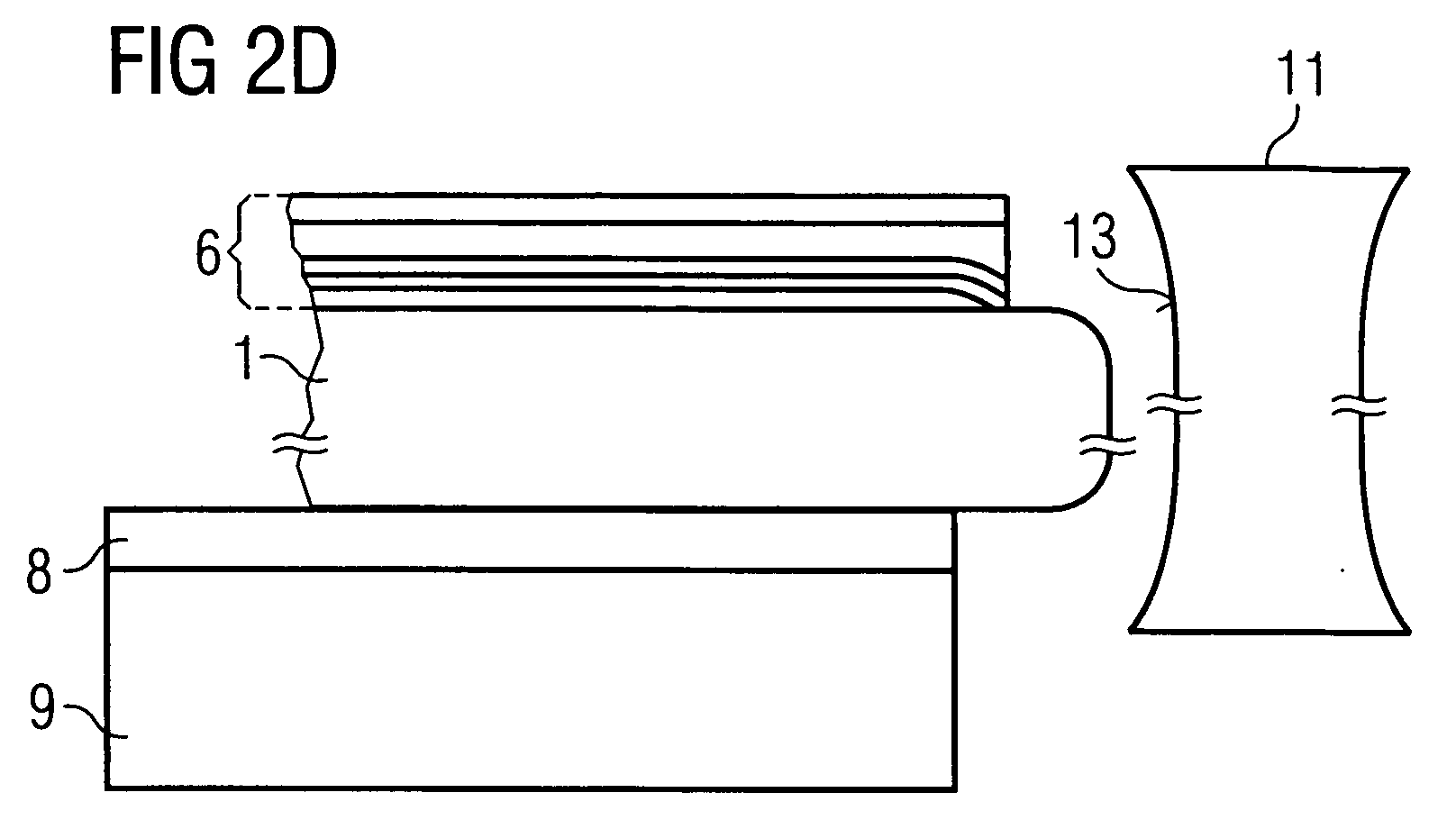
Figur 2 zeigt anhand von Teilschnitten schematisch den erfindungsgemäßen
Verfahrensablauf zum Dünnen eines Wafers. Die
nachfolgenden Nummerierungen entsprechen jeweils den entsprechenden
Teilen der Figur 2:
Durch die Formgestaltung des Randes 5 geht auch eine Reduzierung
des Waferdurchmessers D3 einher, jedoch ist dies unerheblich
für die in den Wafern 1 angeordneten Halbleiterbauelemente,
da der Abtrag am Rand im Vergleich zum Waferdurchmesser
D3 verschwindend gering ist. Der am Rand 5 abgetragene
Bereich bewegt sich typischerweise im Bereich von etwa 1 - 2
mm, was bei heute gängigen Waferdurchmessern D3 von 150, 200
bzw. 300 mm nicht weiter ins Gewicht fällt.A reduction is also possible due to the shape of the
Die mit der Randbearbeitung bzw. Randformung einhergehende Reduzierung des Waferdurchmessers D4 kann für die nachfolgenden Prozessschritte, so z.B. Implantation, Bedampfung, Sputtern, Tempern, etc. durch geeignete Modifikation der entsprechenden Fertigungsanlagen kompensiert werden. Hier kann es unter Umständen erforderlich sein, die Halterungen in diesen Fertigungsanlagen, die der Aufnahme der Wafer dienen, so auszulegen, dass sie für Wafer mit geringfügig geringeren Durchmessern D4 ebenfalls ausgelegt sind.The associated with the edge processing or edge shaping Reduction of the wafer diameter D4 can be used for the following Process steps, e.g. Implantation, vapor deposition, sputtering, Annealing, etc. by appropriate modification of the corresponding Manufacturing systems are compensated. Here it can The brackets in these may be required To design manufacturing plants that serve to hold the wafers that they are for wafers with slightly smaller diameters D4 are also designed.
Zusammenfassend kann festgestellt werden, dass durch ein geringfügiges Abtragen des Randes eines Wafers dieser beim nachfolgenden Dünnen auf sehr einfache, jedoch nichts desto trotz sehr effektive Weise vor flatternden Waferrändern und Randausbrüchen bewahrt werden kann.In summary, it can be said that a minor Removing the edge of a wafer this subsequent thin on very simple, however none the less despite very effective way in front of fluttering wafer edges and Edge breakouts can be preserved.
Die vorliegende Erfindung wurde anhand der vorstehenden Ausführungsbeispielen so dargestellt, um das Prinzip der Erfindung und dessen praktische Anwendung bestmöglichst darzulegen, jedoch lässt sich die Erfindung selbstverständlich bei geeigneter Abwandlung in mannigfaltigen anderen Ausführungsformen realisieren. The present invention has been achieved using the above exemplary embodiments so represented the principle of the invention and to best demonstrate its practical application, however, the invention can of course be used suitable modification in various other embodiments realize.
- 11
- Waferwafer
- 1'1'
- dünner Waferthin wafer
- 22
- erste Oberfläche, Scheibenvorderseitefirst surface, disc front
- 33
- zweite Oberfläche, Scheibenrückseitesecond surface, rear of pane
- 44
- innerer Bereich des Wafersinner area of the wafer
- 55
- Randbereich/Rand des WafersEdge area / edge of the wafer
- 66
- Schichtenlayers
- 77
- nicht bedeckter Randbereichuncovered edge area
- 88th
- Klebeschicht, klebende FolieAdhesive layer, adhesive film
- 99
- (Vakuum-)Chuck(Vacuum) Chuck
- 1010
- Waferanordnungwafer assembly
- 1111
- Schleifradgrinding wheel
- 1212
- Außenfläche am Rand des WafersOuter surface at the edge of the wafer
- 1313
- schleifende Oberfläche des Schleifradesgrinding surface of the grinding wheel
- 1414
- Außenfläche der SchichtOuter surface of the layer
- 1515
- Klebeschicht, klebende FolieAdhesive layer, adhesive film
- 1616
- (Vakuum-)Chuck(Vacuum) Chuck
- 2020
- Randflattern des WafersEdge flutter of the wafer
- 2121
- Rand-/KantenausbruchEdge / Edge outbreak
- 2222
- Stufestep
- D1, D2D1, D2
- Dicke des WafersThickness of the wafer
- D3, D4D3, D4
- Durchmesser des WafersDiameter of the wafer
- D5D5
- Dicke der SchichtThickness of the layer
Claims (9)
dadurch gekennzeichnet, dass der Abtrageschritt (c) durch Abschleifen mittels eines um den Randbereich (5) umlaufenden Schleifrades (11) erfolgt.Method according to claim 1,
characterized in that the removal step (c) is carried out by grinding by means of a grinding wheel (11) rotating around the edge region (5).
dadurch gekennzeichnet, dass das Schleifrad (11) eine zumindest teilweise konkav ausgebildete Schleifoberfläche (13) aufweist.Method according to claim 2,
characterized in that the grinding wheel (11) has an at least partially concave grinding surface (13).
dadurch gekennzeichnet, dass der Randbereich (5) sowie die darauf aufgebrachte mindestens eine Schicht (6) nach dem Abtrageschritt (c) eine durchgehende Außenfläche (12, 14) ausbildet.Method according to one of the preceding claims,
characterized in that the edge region (5) and the at least one layer (6) applied thereon form a continuous outer surface (12, 14) after the removal step (c).
dadurch gekennzeichnet, dass die Randabtragung unter Zuhilfenahme eines Laser mit hoher Laserstrahlleistung erfolgt.Method according to one of the preceding claims,
characterized in that the edge removal is carried out with the aid of a laser with high laser beam power.
dadurch gekennzeichnet, dass die Randabtragung unter Zuhilfenahme eines fokussierten Wasserstrahls mit hoher Wasserstrahlgeschwindigkeit erfolgt.Method according to one of the preceding claims,
characterized in that the edge removal is carried out with the aid of a focused water jet at a high water jet speed.
dadurch gekennzeichnet, dass zur Randabtragung ein Polierfilzmittel mit abtragender Eigenschaft vorgesehen ist.Method according to one of the preceding claims,
characterized in that a polishing felt means with ablative property is provided for edge removal.
dadurch gekennzeichnet, dass der Wafer (1) vor dem Dünnschleifen (d) und/oder vor dem Abtrageprozess (c) auf einen elektrostatischen Chuck (9, 16) gelegt wird.Method according to one of the preceding claims,
characterized in that the wafer (1) is placed on an electrostatic chuck (9, 16) before the thin grinding (d) and / or before the removal process (c).
dadurch gekennzeichnet, dass der Wafer (1) nach dem Dünnschleifen (d) eine Dicke (D2) von weniger als 140µm, insbesondere von weniger als 70µm, aufweist.Method according to one of the preceding claims,
characterized in that after the thin grinding (d) the wafer (1) has a thickness (D2) of less than 140 μm, in particular less than 70 μm.
Applications Claiming Priority (2)
| Application Number | Priority Date | Filing Date | Title |
|---|---|---|---|
| DE10220647A DE10220647C1 (en) | 2002-05-08 | 2002-05-08 | Semiconductor wafer peripheral edge shaping method has material removed from peripheral edge of wafer until surface layer applied to inner part of one of its major surfaces is reached |
| DE10220647 | 2002-05-08 |
Publications (2)
| Publication Number | Publication Date |
|---|---|
| EP1361602A2 true EP1361602A2 (en) | 2003-11-12 |
| EP1361602A3 EP1361602A3 (en) | 2011-01-05 |
Family
ID=27618849
Family Applications (1)
| Application Number | Title | Priority Date | Filing Date |
|---|---|---|---|
| EP03009260A Withdrawn EP1361602A3 (en) | 2002-05-08 | 2003-04-23 | Method for shaping a periphal edge of a wafer |
Country Status (2)
| Country | Link |
|---|---|
| EP (1) | EP1361602A3 (en) |
| DE (1) | DE10220647C1 (en) |
Cited By (3)
| Publication number | Priority date | Publication date | Assignee | Title |
|---|---|---|---|---|
| WO2007107176A1 (en) * | 2006-03-17 | 2007-09-27 | Freescale Semiconductor, Inc. | Method of reducing risk of delamination of a layer of a semiconductor device |
| US7988794B2 (en) | 2007-02-07 | 2011-08-02 | Infineon Technologies Ag | Semiconductor device and method |
| CN113182971A (en) * | 2021-05-12 | 2021-07-30 | 四川雅吉芯电子科技有限公司 | High-precision edge grinding device for monocrystalline silicon epitaxial wafer |
Families Citing this family (2)
| Publication number | Priority date | Publication date | Assignee | Title |
|---|---|---|---|---|
| DE102007011513B3 (en) * | 2007-03-09 | 2008-10-23 | Peter Wolters Gmbh | Method for profiling the peripheral edge of a semiconductor wafer |
| FR2995136B1 (en) | 2012-09-04 | 2015-06-26 | Soitec Silicon On Insulator | PSEUDO-SUBSTRATE WITH IMPROVED EFFICIENCY OF USE OF MONOCRYSTALLINE MATERIAL |
Family Cites Families (6)
| Publication number | Priority date | Publication date | Assignee | Title |
|---|---|---|---|---|
| JPH0719737B2 (en) * | 1990-02-28 | 1995-03-06 | 信越半導体株式会社 | Manufacturing method of S01 substrate |
| JPH0636413B2 (en) * | 1990-03-29 | 1994-05-11 | 信越半導体株式会社 | Manufacturing method of semiconductor element forming substrate |
| US6113721A (en) * | 1995-01-03 | 2000-09-05 | Motorola, Inc. | Method of bonding a semiconductor wafer |
| JPH0964321A (en) * | 1995-08-24 | 1997-03-07 | Komatsu Electron Metals Co Ltd | Method for manufacturing SOI substrate |
| US6162702A (en) * | 1999-06-17 | 2000-12-19 | Intersil Corporation | Self-supported ultra thin silicon wafer process |
| US6328641B1 (en) * | 2000-02-01 | 2001-12-11 | Advanced Micro Devices, Inc. | Method and apparatus for polishing an outer edge ring on a semiconductor wafer |
-
2002
- 2002-05-08 DE DE10220647A patent/DE10220647C1/en not_active Expired - Fee Related
-
2003
- 2003-04-23 EP EP03009260A patent/EP1361602A3/en not_active Withdrawn
Cited By (4)
| Publication number | Priority date | Publication date | Assignee | Title |
|---|---|---|---|---|
| WO2007107176A1 (en) * | 2006-03-17 | 2007-09-27 | Freescale Semiconductor, Inc. | Method of reducing risk of delamination of a layer of a semiconductor device |
| US7988794B2 (en) | 2007-02-07 | 2011-08-02 | Infineon Technologies Ag | Semiconductor device and method |
| CN113182971A (en) * | 2021-05-12 | 2021-07-30 | 四川雅吉芯电子科技有限公司 | High-precision edge grinding device for monocrystalline silicon epitaxial wafer |
| CN113182971B (en) * | 2021-05-12 | 2022-11-25 | 四川雅吉芯电子科技有限公司 | High-precision edge grinding device for monocrystalline silicon epitaxial wafer |
Also Published As
| Publication number | Publication date |
|---|---|
| EP1361602A3 (en) | 2011-01-05 |
| DE10220647C1 (en) | 2003-08-21 |
Similar Documents
| Publication | Publication Date | Title |
|---|---|---|
| DE69507990T2 (en) | Method and device for mirror polishing a part of a wafer | |
| DE10195941B4 (en) | Semiconductor processing method for removing conductive material | |
| DE102012214817B4 (en) | Method for producing a semiconductor device | |
| DE102006018644B4 (en) | Processing method for a semiconductor wafer | |
| DE69723338T2 (en) | Process for the production of semiconductor wafers | |
| DE102006030866B4 (en) | Processing method for a semiconductor wafer | |
| DE19626396B4 (en) | Method and device for producing and grinding silicon wafers | |
| DE102017212858B4 (en) | Method for processing a substrate | |
| DE102005014539B4 (en) | Wafer processing method | |
| DE102010003600B4 (en) | Wafer processing method | |
| DE102009038942B4 (en) | Device for machining flat workpieces on both sides and method for machining a plurality of semiconductor wafers simultaneously by removing material from both sides | |
| DE102015208897A1 (en) | Wafer processing method | |
| DE3335116A1 (en) | SEMICONDUCTOR BOARDS AND METHOD AND DEVICE FOR THEIR PRODUCTION | |
| DE3784758T2 (en) | Manufacturing process for EPROM cells with oxide-nitride-oxide dielectric. | |
| DE102019218374A1 (en) | PROCESSING METHOD FOR A WAFER | |
| EP1829986B1 (en) | Method for treating surfaces of a hard carbon coating | |
| DE102015115914B4 (en) | Wafer arrangement comprising a wafer and a wafer holding ring | |
| DE69029913T2 (en) | Process for treating a substrate for semiconductor components | |
| DE10333810B4 (en) | Method for processing a semiconductor wafer including grinding the backside | |
| DE60008985T2 (en) | Preparation of a chemical-mechanical polishing sheet and method | |
| DE102015002542A1 (en) | Wafer dividing method | |
| DE102010040441B4 (en) | Manufacturing method of a semiconductor device | |
| DE102006020823B4 (en) | Process for producing a polished semiconductor wafer | |
| DE102019204974A1 (en) | WAFER PROCESSING PROCEDURES | |
| DE10220647C1 (en) | Semiconductor wafer peripheral edge shaping method has material removed from peripheral edge of wafer until surface layer applied to inner part of one of its major surfaces is reached |
Legal Events
| Date | Code | Title | Description |
|---|---|---|---|
| PUAI | Public reference made under article 153(3) epc to a published international application that has entered the european phase |
Free format text: ORIGINAL CODE: 0009012 |
|
| AK | Designated contracting states |
Kind code of ref document: A2 Designated state(s): AT BE BG CH CY CZ DE DK EE ES FI FR GB GR HU IE IT LI LU MC NL PT RO SE SI SK TR |
|
| AX | Request for extension of the european patent |
Extension state: AL LT LV MK |
|
| RAP1 | Party data changed (applicant data changed or rights of an application transferred) |
Owner name: INFINEON TECHNOLOGIES AG |
|
| PUAL | Search report despatched |
Free format text: ORIGINAL CODE: 0009013 |
|
| AK | Designated contracting states |
Kind code of ref document: A3 Designated state(s): AT BE BG CH CY CZ DE DK EE ES FI FR GB GR HU IE IT LI LU MC NL PT RO SE SI SK TR |
|
| AX | Request for extension of the european patent |
Extension state: AL LT LV MK |
|
| AKY | No designation fees paid | ||
| REG | Reference to a national code |
Ref country code: DE Ref legal event code: R108 |
|
| REG | Reference to a national code |
Ref country code: DE Ref legal event code: R108 Effective date: 20110907 |
|
| STAA | Information on the status of an ep patent application or granted ep patent |
Free format text: STATUS: THE APPLICATION IS DEEMED TO BE WITHDRAWN |
|
| 18D | Application deemed to be withdrawn |
Effective date: 20110706 |