EP1361427A2 - Vorrichtung und Verfahren zur Abbildung spezifischer Elemente mittels Röntgenstrahlen - Google Patents
Vorrichtung und Verfahren zur Abbildung spezifischer Elemente mittels Röntgenstrahlen Download PDFInfo
- Publication number
- EP1361427A2 EP1361427A2 EP03001969A EP03001969A EP1361427A2 EP 1361427 A2 EP1361427 A2 EP 1361427A2 EP 03001969 A EP03001969 A EP 03001969A EP 03001969 A EP03001969 A EP 03001969A EP 1361427 A2 EP1361427 A2 EP 1361427A2
- Authority
- EP
- European Patent Office
- Prior art keywords
- filter
- rays
- energy
- ray
- image
- Prior art date
- Legal status (The legal status is an assumption and is not a legal conclusion. Google has not performed a legal analysis and makes no representation as to the accuracy of the status listed.)
- Withdrawn
Links
Images
Classifications
-
- G—PHYSICS
- G01—MEASURING; TESTING
- G01N—INVESTIGATING OR ANALYSING MATERIALS BY DETERMINING THEIR CHEMICAL OR PHYSICAL PROPERTIES
- G01N23/00—Investigating or analysing materials by the use of wave or particle radiation, e.g. X-rays or neutrons, not covered by groups G01N3/00 – G01N17/00, G01N21/00 or G01N22/00
- G01N23/02—Investigating or analysing materials by the use of wave or particle radiation, e.g. X-rays or neutrons, not covered by groups G01N3/00 – G01N17/00, G01N21/00 or G01N22/00 by transmitting the radiation through the material
- G01N23/06—Investigating or analysing materials by the use of wave or particle radiation, e.g. X-rays or neutrons, not covered by groups G01N3/00 – G01N17/00, G01N21/00 or G01N22/00 by transmitting the radiation through the material and measuring the absorption
- G01N23/083—Investigating or analysing materials by the use of wave or particle radiation, e.g. X-rays or neutrons, not covered by groups G01N3/00 – G01N17/00, G01N21/00 or G01N22/00 by transmitting the radiation through the material and measuring the absorption the radiation being X-rays
-
- G—PHYSICS
- G01—MEASURING; TESTING
- G01N—INVESTIGATING OR ANALYSING MATERIALS BY DETERMINING THEIR CHEMICAL OR PHYSICAL PROPERTIES
- G01N23/00—Investigating or analysing materials by the use of wave or particle radiation, e.g. X-rays or neutrons, not covered by groups G01N3/00 – G01N17/00, G01N21/00 or G01N22/00
- G01N23/02—Investigating or analysing materials by the use of wave or particle radiation, e.g. X-rays or neutrons, not covered by groups G01N3/00 – G01N17/00, G01N21/00 or G01N22/00 by transmitting the radiation through the material
- G01N23/04—Investigating or analysing materials by the use of wave or particle radiation, e.g. X-rays or neutrons, not covered by groups G01N3/00 – G01N17/00, G01N21/00 or G01N22/00 by transmitting the radiation through the material and forming images of the material
Definitions
- the present invention relates to x-ray imaging, and more particularly, to x-ray imaging techniques that can distinguish different elemental substances within the object being imaged.
- x-ray transmission imaging illumination is projected through an object and the imaging signal results from a subtractive process, i.e. what is imaged is the far field of the illuminations minus any signal that was absorbed, reflected or scattered.
- x-ray inspection is being used routinely for inspection of products in the manufacturing environments. Many of these applications require that a particular material be examined in the inspection process in spite of the presence of other materials that also absorb x-rays.
- surface mounted integrated circuits are examined during manufacture to determine the distribution of solder on the assembly, which in turn, is related to the reliability of the assembly. In such systems, Cu traces, Si chips, and Fe in transformers all conspire to obscure, or 'shadow' the solder joints.
- the desired specificity can be provided by using a single energy source with a detector that has the ability to detect the energies of the x-rays that reach the detector.
- a detector that has the ability to detect the energies of the x-rays that reach the detector.
- US 5,943,388 describes a discrete detector for use with a broad energy range polychromatic illumination source.
- active pixels are created by discrete detectors coupled to a multi-channel analyzer that detects each x-ray photon arriving at each pixel. The photons are counted in bins corresponding to a pre-defined set of energy windows. Each energy window corresponds to a different image.
- By correctly choosing energy windows that are specifically affected by particular materials significant improvements in specificity can be achieved.
- the cost of the detectors for such a scheme significantly increases the cost of the imaging systems.
- the present invention is an apparatus for imaging features of an object constructed from a material that includes a first element in the presence of features constructed from a material that includes a second element.
- the apparatus utilizes a filtered x-ray spectrum to image the object with the aid of an x-ray detector.
- the filtered x-ray spectrum is generated from a polychromatic x-ray source having a maximum energy that is determined by the absorption spectrum of the first element.
- the filter includes a filter element having a dominant absorption edge greater than or equal to the dominant absorption edge of the second element and less than the maximum energy. The filter removes x-rays that would otherwise be absorbed by the second element thereby improving the direct interpretation of contrast of images based on x-ray absorption of the first element.
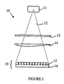
- Imaging system 10 utilizes a conventional polychromatic x-ray energy source 11, which generates a useful cone of x-rays 12.
- the x-rays from source 11 are filtered by a filter 13 before impinging on the object 14.
- the manner in which this filter is constructed will be discussed in more detail below.
- the x-ray energy leaving the object at various points is detected by a pixelated, or 'imaging', x-ray detector 19.
- a detector for example could include an x-ray detection material 15 that converts the x-rays incident thereon to visible light that is detected by a camera chip 16. Any imaging x-ray sensor, x-ray camera or the like can be used for this invention.
- the manner in which this arrangement provides improved specificity can be more easily understood with reference to an imaging problem in which a heavy, or high atomic number, element, e.g., Pb, must be distinguished from a lighter, or lower atomic number, element, e.g. Cu.
- the present invention is based on the observation that for any given material and thickness combination, the images formed by an x-ray system depend on the energy spectrum generated by the x-ray source. In general, the x-ray spectrum provided by inexpensive x-ray sources is far from optimum for imaging features constructed from a high atomic number element in the presence of features constructed from a lower atomic number element.
- the present invention utilizes a filter to modify the spectrum of an x-ray source in a manner that enhances its ability to image specific elements in the presence of interfering elements.
- Pb has a feature at the K-edge of about 87.9 keV
- Cu has a K-edge of about 8.98 keV.
- These features can be utilized to enhance image contrast.
- a source spectrum with enhanced flux between the K-edge of Pb and an energy of about 140keV will greatly improve Pb contrast in the presence of Cu in an image taken using this spectrum.
- any dominant absorption edge or other significant absorbing feature in the absorption spectrum of the desired element in an energy range where the interfering element has reduced absorption may be utilized to improve the contrast of the desired element.
- a conventional polychromatic x-ray source designed to maximize x-ray flux available for image formation is typically based on Brehmstrahlung radiation.
- Such sources have a characteristic broad energy distribution that may encompass many absorbing features and extend somewhat beyond the higher significant absorbing feature.
- the upper limit of the source spectrum is fixed by the choice of x-ray tube operating voltage so that some of the flux is absorbed by the core shell edge of the higher atomic number element to create contrast related to the distribution of that element in the object.
- Unfortunately, such a spectrum has a significant number of photons at lower energies, and hence, the low atomic number element absorbs a significant amount of the source energy and obscures the material from the higher atomic number element.
- the intensity of the image at this pixel is proportional to the number of x-rays that pass through the object being imaged and reach the detector responsible for this pixel.
- N the total number of x-rays that pass through the pixel during an exposure with no object in place.
- N L the number of x-rays reaching the detector is reduced by the x-rays that are absorbed by the Cu, denoted by N L and by the x-rays that are absorbed by the Pb, denoted by N H .
- any element that absorbs x-rays from the source contributes to the contrast.
- the Cu selectively absorbs x-rays with energies just below the Cu dominant absorption edge.
- the Pb selectively absorbs x-rays with energies just above the Pb k-edge, which is the significant absorbing feature for Pb.
- the present invention is based on the observation that the contrast caused by the Cu would be significantly reduced if the source did not include x-ray energies that are readily absorbed by the Cu.
- filter 13 discussed above is included in the imaging apparatus to absorb x-rays that would normally be absorbed by the Cu.
- the filter can be constructed from any material having a dominant absorption edge at or above that of the Cu and below the dominant absorption edge or other significant absorbing feature of the Pb.
- a material having a dominant absorption edge between that of the interfering material and that of the desired material is utilized. While Cu could be used for the filter in the case in which Cu is the interfering element, the dominant absorption edge of Cu is not absolutely sharp. Accordingly, some of the x-rays at energies around the Cu dominant absorption edge would leak through the filter. Hence, an element having a dominant absorption edge at a higher energy is utilized to assure that photons that would be absorbed by Cu are effectively removed.
- the choice of material depends on the ability to provide an effective economical filter. Bulk material cost, mechanical properties suitable for forming thin plate, low toxicity and reactivity, and corrosion resistance are factors in the choice of materials. For Cu imaging in the presence of Pb, a convenient choice is Mo, since other materials between Cu and Mo are more expensive and more difficult to handle.
- the present invention can also be utilized for enhancing the image of any structure constructed from a material partially or entirely composed of a first element, the "heavy" or high atomic number element, in the presence of a material partially or entirely composed of a second, "lighter” or lower atomic number element.
- the filter is constructed from a material having a dominant absorption edge energy that is less than the energy of the absorbing feature of the absorption spectrum of the heavy element that is to be exploited and greater than or equal to the energy of the dominant absorption edge of the lighter interfering element.
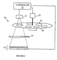
- Apparatus 50 includes a mechanism 22 that rotates a wheel 24 having a plurality of filter elements 23.
- the filter elements are rotated into the beam from x-ray source 21.
- Image detector 19 forms an image of object 14 with each filter in place.
- the acceleration potential in the x-ray source would remain constant; this is the preferred embodiment for applications where this provides adequate specificity.
- the acceleration potential in x-ray source 21 can be adjusted for each filter element such that the x-ray spectrum leaving the filter element is peaked at some energy between the dominant absorption edge of the filter material and the high energy end of the spectrum from source 21.
- each image is selectively enhanced for elements having a significant absorbing feature within the energy range provided at the exit side of the filter.
- interference from elements having significant absorbing features at higher energies can also be present.
- This interference can be removed by combining a number of different images, each taken with a different filter and energy spectrum. For example, if there are 5 elements of interest in object 14, weighted combinations of the corresponding pixels in each of 5 images can be used to determine the concentration of each element seen by that pixel, and hence, create images based on each element. The weight factors depend on the efficiency with which each element contributes to each image when a particular filter and energy spectrum is used.
- images with sufficient elemental specificity can be formed from weighted sums of the raw images taken with various filters
- the endpoint need not be altered.
- the weighting coefficients used in the various linear combinations of the images can take this information into account.
- a difference image is formed between two images taken with different filters, the image that would have resulted from the lower energy filter and a reduced energy x-ray source is obtained.
- wheel 24 may include gaps to aid in the calibration of the x-ray source/detector combination and provide an unfiltered reference image.
- the x-ray source must have sufficient intensity at energies around the significant absorbing feature of the desired element. Hence, the source is adjusted to provide a spectrum that extends above the significant absorbing feature of the desired element sufficiently to provide good imaging.
- the optimum thickness for such a filter depends on a tradeoff between increasing contrast between the high and low atomic number elements while still leaving a sufficient number of x-ray photons capable of imaging the high atomic number elements. This is necessary because even a well-chosen material does in fact absorb somewhat above a dominant absorption edge of the high atomic number material.
- filter thicknesses of 250 - 3000 ⁇ m have proven useful, with a likely optimum in the 500 ⁇ m or 20 mil range.
Landscapes
- Health & Medical Sciences (AREA)
- General Health & Medical Sciences (AREA)
- Life Sciences & Earth Sciences (AREA)
- Chemical & Material Sciences (AREA)
- Analytical Chemistry (AREA)
- Biochemistry (AREA)
- Physics & Mathematics (AREA)
- General Physics & Mathematics (AREA)
- Immunology (AREA)
- Pathology (AREA)
- Toxicology (AREA)
- Analysing Materials By The Use Of Radiation (AREA)
- Apparatus For Radiation Diagnosis (AREA)
Applications Claiming Priority (2)
| Application Number | Priority Date | Filing Date | Title |
|---|---|---|---|
| US10/140,617 US6597758B1 (en) | 2002-05-06 | 2002-05-06 | Elementally specific x-ray imaging apparatus and method |
| US140617 | 2002-05-06 |
Publications (2)
| Publication Number | Publication Date |
|---|---|
| EP1361427A2 true EP1361427A2 (de) | 2003-11-12 |
| EP1361427A3 EP1361427A3 (de) | 2004-01-14 |
Family
ID=22492048
Family Applications (1)
| Application Number | Title | Priority Date | Filing Date |
|---|---|---|---|
| EP03001969A Withdrawn EP1361427A3 (de) | 2002-05-06 | 2003-01-30 | Vorrichtung und Verfahren zur Abbildung spezifischer Elemente mittels Röntgenstrahlen |
Country Status (2)
| Country | Link |
|---|---|
| US (1) | US6597758B1 (de) |
| EP (1) | EP1361427A3 (de) |
Families Citing this family (23)
| Publication number | Priority date | Publication date | Assignee | Title |
|---|---|---|---|---|
| US6751294B1 (en) * | 2002-08-08 | 2004-06-15 | Advanced Micro Devices, Inc. | Prevention of parametic or functional changes to silicon semiconductor device properties during x-ray inspection |
| US7046756B2 (en) * | 2003-05-20 | 2006-05-16 | General Electric Company | Rotatable filter for a pre-subject CT collimator having multiple filtering profiles |
| US6968030B2 (en) * | 2003-05-20 | 2005-11-22 | General Electric Company | Method and apparatus for presenting multiple pre-subject filtering profiles during CT data acquisition |
| US7120222B2 (en) * | 2003-06-05 | 2006-10-10 | General Electric Company | CT imaging system with multiple peak x-ray source |
| US20060133575A1 (en) * | 2004-12-21 | 2006-06-22 | Advanced X-Ray Technology, Inc. | X-ray needle apparatus and method for radiation treatment |
| US7330535B2 (en) * | 2005-11-10 | 2008-02-12 | General Electric Company | X-ray flux management device |
| CN101074937B (zh) * | 2006-05-19 | 2010-09-08 | 清华大学 | 能谱调制装置、识别材料的方法和设备及图像处理方法 |
| SE530009C2 (sv) * | 2006-06-01 | 2008-02-05 | Metso Paper Inc | Anordning för uppriktning av en malapparats maldon |
| US7593502B2 (en) * | 2006-10-13 | 2009-09-22 | General Electric Company | Methods and apparatus for fast rotation speed scanners |
| CN101303909B (zh) * | 2007-05-11 | 2013-03-27 | Ge医疗系统环球技术有限公司 | 滤波器单元,x射线管单元和x射线成像系统 |
| US8194820B2 (en) * | 2009-02-06 | 2012-06-05 | The Board Of Trustees Of The Leland Stanford Junior University | Optimal weights for measuring spectral x-ray data |
| JP5564303B2 (ja) * | 2009-06-12 | 2014-07-30 | 株式会社日立ハイテクサイエンス | X線透過検査装置 |
| US9101272B2 (en) * | 2011-03-24 | 2015-08-11 | Jefferson Radiology, P.C. | Fixed anterior gantry CT shielding |
| JP2013156172A (ja) * | 2012-01-31 | 2013-08-15 | X-Ray Precision Inc | X線検査装置 |
| DE102012219051A1 (de) * | 2012-10-18 | 2014-04-24 | Klinikum Der Universität München | Auswahl eines Strahlungsformfilters |
| JP6266284B2 (ja) * | 2013-09-19 | 2018-01-24 | 東芝メディカルシステムズ株式会社 | X線診断装置 |
| DE102014203465B4 (de) * | 2014-02-26 | 2026-05-07 | Siemens Healthineers Ag | Auswahl eines Strahlungsformfilters aus einer Mehrzahl von Strahlungsformfiltern |
| JP6397690B2 (ja) * | 2014-08-11 | 2018-09-26 | 株式会社日立ハイテクノロジーズ | X線透過検査装置及び異物検出方法 |
| US9991014B1 (en) * | 2014-09-23 | 2018-06-05 | Daniel Gelbart | Fast positionable X-ray filter |
| JP2016090494A (ja) * | 2014-11-10 | 2016-05-23 | 株式会社 オプトメカトロ | X線検査装置 |
| CN105433973B (zh) * | 2015-12-30 | 2018-09-18 | 沈阳东软医疗系统有限公司 | Ct扫描设备、ct系统和控制过滤器组件的方法及装置 |
| US10634797B2 (en) * | 2017-07-07 | 2020-04-28 | International Business Machines Corporation | Real time X-ray dosimeter using diodes with variable thickness degrader |
| CN111657989A (zh) * | 2020-07-09 | 2020-09-15 | 汕头市超声仪器研究所有限公司 | 一种从接收端降低x射线检测环境辐射的方法 |
Family Cites Families (4)
| Publication number | Priority date | Publication date | Assignee | Title |
|---|---|---|---|---|
| EP0081227B1 (de) * | 1981-12-07 | 1987-03-18 | Albert Macovski | Energieselektives Röntgenaufnahme- und Wiedergabesystem |
| US4910757A (en) * | 1987-11-06 | 1990-03-20 | Hitachi, Ltd. | Method and apparatus for X-ray imaging |
| US4945552A (en) * | 1987-12-04 | 1990-07-31 | Hitachi, Ltd. | Imaging system for obtaining X-ray energy subtraction images |
| US5943388A (en) * | 1996-07-30 | 1999-08-24 | Nova R & D, Inc. | Radiation detector and non-destructive inspection |
-
2002
- 2002-05-06 US US10/140,617 patent/US6597758B1/en not_active Expired - Fee Related
-
2003
- 2003-01-30 EP EP03001969A patent/EP1361427A3/de not_active Withdrawn
Also Published As
| Publication number | Publication date |
|---|---|
| EP1361427A3 (de) | 2004-01-14 |
| US6597758B1 (en) | 2003-07-22 |
Similar Documents
| Publication | Publication Date | Title |
|---|---|---|
| US6597758B1 (en) | Elementally specific x-ray imaging apparatus and method | |
| Ballabriga et al. | The Medipix3RX: a high resolution, zero dead-time pixel detector readout chip allowing spectroscopic imaging | |
| US5754621A (en) | X-ray inspection method and apparatus, prepreg inspecting method, and method for fabricating multi-layer printed circuit board | |
| US8111803B2 (en) | Method for energy sensitive computed tomography using checkerboard filtering | |
| US9048061B2 (en) | X-ray scanners and X-ray sources therefor | |
| CN1656373B (zh) | 元素特定的x射线荧光显微镜以及操作方法 | |
| US6650730B2 (en) | Filter assembly for X-ray filter system for medical imaging contrast enhancement | |
| JP5297142B2 (ja) | 異物検出方法および装置 | |
| RU2344885C2 (ru) | Устройство и способ разделения навалочных материалов | |
| EP3358375B1 (de) | Röntgenbilderfassungssystem und röntgenbilderfassungsverfahren | |
| US7218706B2 (en) | Energy discrimination radiography systems and methods for inspecting industrial components | |
| DE102011108876B4 (de) | Direktwandelnder Röntgendetektor mit Strahlenschutz für die Elektronik | |
| EP2690432A1 (de) | Röngtenspektroskopietechnik mit zusammengeführten Spektraldaten | |
| Zielińska et al. | X-ray fluorescence imaging system for fast mapping of pigment distributions in cultural heritage paintings | |
| JPH0743320A (ja) | X線検査方法およびその装置並びにプレプレグの検査方法および多層配線基板の製造方法 | |
| CN111801600B (zh) | 多谱x射线探测器 | |
| US8081732B2 (en) | Correcting transverse scattering in a multi-emitter CT scanner | |
| Roque et al. | Sub-pixel energy-weighting techniques for metallic contaminant highlighting in a pharmaceutical hard capsule using a Timepix3 CdZnTe hybrid pixel detector | |
| Blish et al. | Filter optimization for X-ray inspection of surface-mounted ICs | |
| Benedetti et al. | Identifying, quantifying, and mitigating background with the time-resolved x-ray diffraction platform at NIF | |
| Blue et al. | Improved pinhole-apertured point-projection backlighter geometry | |
| Adams | X-ray laminography analysis of ultra-fine-pitch solder connections on ultrathin boards | |
| WO1997033160A1 (de) | Verfahren und vorrichtung zur automatischen radioskopischen qualitätskontrolle von nahrungsmitteln | |
| TWI747101B (zh) | 製程監測 | |
| JPH0827245B2 (ja) | X線撮像方法及びその装置 |
Legal Events
| Date | Code | Title | Description |
|---|---|---|---|
| PUAI | Public reference made under article 153(3) epc to a published international application that has entered the european phase |
Free format text: ORIGINAL CODE: 0009012 |
|
| AK | Designated contracting states |
Kind code of ref document: A2 Designated state(s): AT BE BG CH CY CZ DE DK EE ES FI FR GB GR HU IE IT LI LU MC NL PT SE SI SK TR |
|
| AX | Request for extension of the european patent |
Extension state: AL LT LV MK RO |
|
| PUAL | Search report despatched |
Free format text: ORIGINAL CODE: 0009013 |
|
| AK | Designated contracting states |
Kind code of ref document: A3 Designated state(s): AT BE BG CH CY CZ DE DK EE ES FI FR GB GR HU IE IT LI LU MC NL PT SE SI SK TR |
|
| AX | Request for extension of the european patent |
Extension state: AL LT LV MK RO |
|
| RIC1 | Information provided on ipc code assigned before grant |
Ipc: 7G 01N 23/04 B Ipc: 7G 01N 23/08 A |
|
| 17P | Request for examination filed |
Effective date: 20040616 |
|
| AKX | Designation fees paid |
Designated state(s): DE GB |
|
| RAP1 | Party data changed (applicant data changed or rights of an application transferred) |
Owner name: AGILENT TECHNOLOGIES, INC. |
|
| 17Q | First examination report despatched |
Effective date: 20051223 |
|
| STAA | Information on the status of an ep patent application or granted ep patent |
Free format text: STATUS: THE APPLICATION IS DEEMED TO BE WITHDRAWN |
|
| 18D | Application deemed to be withdrawn |
Effective date: 20080801 |