EP1355522A2 - Multilayered wiring board, method of producing multilayered wiring board, electronic device and electronic apparatus - Google Patents
Multilayered wiring board, method of producing multilayered wiring board, electronic device and electronic apparatus Download PDFInfo
- Publication number
- EP1355522A2 EP1355522A2 EP03252346A EP03252346A EP1355522A2 EP 1355522 A2 EP1355522 A2 EP 1355522A2 EP 03252346 A EP03252346 A EP 03252346A EP 03252346 A EP03252346 A EP 03252346A EP 1355522 A2 EP1355522 A2 EP 1355522A2
- Authority
- EP
- European Patent Office
- Prior art keywords
- interlayer insulation
- wiring
- producing
- wiring board
- multilayered
- Prior art date
- Legal status (The legal status is an assumption and is not a legal conclusion. Google has not performed a legal analysis and makes no representation as to the accuracy of the status listed.)
- Withdrawn
Links
Images


Classifications
-
- H—ELECTRICITY
- H05—ELECTRIC TECHNIQUES NOT OTHERWISE PROVIDED FOR
- H05K—PRINTED CIRCUITS; CASINGS OR CONSTRUCTIONAL DETAILS OF ELECTRIC APPARATUS; MANUFACTURE OF ASSEMBLAGES OF ELECTRICAL COMPONENTS
- H05K3/00—Apparatus or processes for manufacturing printed circuits
- H05K3/46—Manufacturing multilayer circuits
- H05K3/4644—Manufacturing multilayer circuits by building the multilayer layer by layer, i.e. build-up multilayer circuits
- H05K3/4647—Manufacturing multilayer circuits by building the multilayer layer by layer, i.e. build-up multilayer circuits by applying an insulating layer around previously made via studs
-
- H—ELECTRICITY
- H05—ELECTRIC TECHNIQUES NOT OTHERWISE PROVIDED FOR
- H05K—PRINTED CIRCUITS; CASINGS OR CONSTRUCTIONAL DETAILS OF ELECTRIC APPARATUS; MANUFACTURE OF ASSEMBLAGES OF ELECTRICAL COMPONENTS
- H05K3/00—Apparatus or processes for manufacturing printed circuits
- H05K3/46—Manufacturing multilayer circuits
- H05K3/4644—Manufacturing multilayer circuits by building the multilayer layer by layer, i.e. build-up multilayer circuits
- H05K3/4664—Adding a circuit layer by thick film methods, e.g. printing techniques or by other techniques for making conductive patterns by using pastes, inks or powders
-
- H—ELECTRICITY
- H05—ELECTRIC TECHNIQUES NOT OTHERWISE PROVIDED FOR
- H05K—PRINTED CIRCUITS; CASINGS OR CONSTRUCTIONAL DETAILS OF ELECTRIC APPARATUS; MANUFACTURE OF ASSEMBLAGES OF ELECTRICAL COMPONENTS
- H05K2203/00—Indexing scheme relating to apparatus or processes for manufacturing printed circuits covered by H05K3/00
- H05K2203/01—Tools for processing; Objects used during processing
- H05K2203/0104—Tools for processing; Objects used during processing for patterning or coating
- H05K2203/013—Inkjet printing, e.g. for printing insulating material or resist
-
- H—ELECTRICITY
- H05—ELECTRIC TECHNIQUES NOT OTHERWISE PROVIDED FOR
- H05K—PRINTED CIRCUITS; CASINGS OR CONSTRUCTIONAL DETAILS OF ELECTRIC APPARATUS; MANUFACTURE OF ASSEMBLAGES OF ELECTRICAL COMPONENTS
- H05K3/00—Apparatus or processes for manufacturing printed circuits
- H05K3/10—Apparatus or processes for manufacturing printed circuits in which conductive material is applied to the insulating support in such a manner as to form the desired conductive pattern
- H05K3/12—Apparatus or processes for manufacturing printed circuits in which conductive material is applied to the insulating support in such a manner as to form the desired conductive pattern using thick film techniques, e.g. printing techniques to apply the conductive material or similar techniques for applying conductive paste or ink patterns
- H05K3/1241—Apparatus or processes for manufacturing printed circuits in which conductive material is applied to the insulating support in such a manner as to form the desired conductive pattern using thick film techniques, e.g. printing techniques to apply the conductive material or similar techniques for applying conductive paste or ink patterns by ink-jet printing or drawing by dispensing
- H05K3/125—Apparatus or processes for manufacturing printed circuits in which conductive material is applied to the insulating support in such a manner as to form the desired conductive pattern using thick film techniques, e.g. printing techniques to apply the conductive material or similar techniques for applying conductive paste or ink patterns by ink-jet printing or drawing by dispensing by ink-jet printing
-
- H—ELECTRICITY
- H05—ELECTRIC TECHNIQUES NOT OTHERWISE PROVIDED FOR
- H05K—PRINTED CIRCUITS; CASINGS OR CONSTRUCTIONAL DETAILS OF ELECTRIC APPARATUS; MANUFACTURE OF ASSEMBLAGES OF ELECTRICAL COMPONENTS
- H05K3/00—Apparatus or processes for manufacturing printed circuits
- H05K3/40—Forming printed elements for providing electric connections to or between printed circuits
- H05K3/4038—Through-connections; Vertical interconnect access [VIA] connections
- H05K3/4053—Through-connections; Vertical interconnect access [VIA] connections by thick-film techniques
- H05K3/4069—Through-connections; Vertical interconnect access [VIA] connections by thick-film techniques for via connections in organic insulating substrates
-
- H—ELECTRICITY
- H10—SEMICONDUCTOR DEVICES; ELECTRIC SOLID-STATE DEVICES NOT OTHERWISE PROVIDED FOR
- H10W—GENERIC PACKAGES, INTERCONNECTIONS, CONNECTORS OR OTHER CONSTRUCTIONAL DETAILS OF DEVICES COVERED BY CLASS H10
- H10W70/00—Package substrates; Interposers; Redistribution layers [RDL]
- H10W70/60—Insulating or insulated package substrates; Interposers; Redistribution layers
- H10W70/62—Insulating or insulated package substrates; Interposers; Redistribution layers characterised by their interconnections
- H10W70/65—Shapes or dispositions of interconnections
- H10W70/654—Top-view layouts
- H10W70/655—Fan-out layouts
-
- H—ELECTRICITY
- H10—SEMICONDUCTOR DEVICES; ELECTRIC SOLID-STATE DEVICES NOT OTHERWISE PROVIDED FOR
- H10W—GENERIC PACKAGES, INTERCONNECTIONS, CONNECTORS OR OTHER CONSTRUCTIONAL DETAILS OF DEVICES COVERED BY CLASS H10
- H10W72/00—Interconnections or connectors in packages
- H10W72/20—Bump connectors, e.g. solder bumps or copper pillars; Dummy bumps; Thermal bumps
-
- H—ELECTRICITY
- H10—SEMICONDUCTOR DEVICES; ELECTRIC SOLID-STATE DEVICES NOT OTHERWISE PROVIDED FOR
- H10W—GENERIC PACKAGES, INTERCONNECTIONS, CONNECTORS OR OTHER CONSTRUCTIONAL DETAILS OF DEVICES COVERED BY CLASS H10
- H10W72/00—Interconnections or connectors in packages
- H10W72/90—Bond pads, in general
- H10W72/921—Structures or relative sizes of bond pads
- H10W72/922—Bond pads being integral with underlying chip-level interconnections
- H10W72/9223—Bond pads being integral with underlying chip-level interconnections with redistribution layers [RDL]
-
- H—ELECTRICITY
- H10—SEMICONDUCTOR DEVICES; ELECTRIC SOLID-STATE DEVICES NOT OTHERWISE PROVIDED FOR
- H10W—GENERIC PACKAGES, INTERCONNECTIONS, CONNECTORS OR OTHER CONSTRUCTIONAL DETAILS OF DEVICES COVERED BY CLASS H10
- H10W72/00—Interconnections or connectors in packages
- H10W72/90—Bond pads, in general
- H10W72/921—Structures or relative sizes of bond pads
- H10W72/923—Bond pads having multiple stacked layers
-
- H—ELECTRICITY
- H10—SEMICONDUCTOR DEVICES; ELECTRIC SOLID-STATE DEVICES NOT OTHERWISE PROVIDED FOR
- H10W—GENERIC PACKAGES, INTERCONNECTIONS, CONNECTORS OR OTHER CONSTRUCTIONAL DETAILS OF DEVICES COVERED BY CLASS H10
- H10W72/00—Interconnections or connectors in packages
- H10W72/90—Bond pads, in general
- H10W72/931—Shapes of bond pads
- H10W72/934—Cross-sectional shape, i.e. in side view
-
- H—ELECTRICITY
- H10—SEMICONDUCTOR DEVICES; ELECTRIC SOLID-STATE DEVICES NOT OTHERWISE PROVIDED FOR
- H10W—GENERIC PACKAGES, INTERCONNECTIONS, CONNECTORS OR OTHER CONSTRUCTIONAL DETAILS OF DEVICES COVERED BY CLASS H10
- H10W72/00—Interconnections or connectors in packages
- H10W72/90—Bond pads, in general
- H10W72/941—Dispositions of bond pads
- H10W72/9415—Dispositions of bond pads relative to the surface, e.g. recessed, protruding
-
- H—ELECTRICITY
- H10—SEMICONDUCTOR DEVICES; ELECTRIC SOLID-STATE DEVICES NOT OTHERWISE PROVIDED FOR
- H10W—GENERIC PACKAGES, INTERCONNECTIONS, CONNECTORS OR OTHER CONSTRUCTIONAL DETAILS OF DEVICES COVERED BY CLASS H10
- H10W72/00—Interconnections or connectors in packages
- H10W72/90—Bond pads, in general
- H10W72/941—Dispositions of bond pads
- H10W72/942—Dispositions of bond pads relative to underlying supporting features, e.g. bond pads, RDLs or vias
-
- Y—GENERAL TAGGING OF NEW TECHNOLOGICAL DEVELOPMENTS; GENERAL TAGGING OF CROSS-SECTIONAL TECHNOLOGIES SPANNING OVER SEVERAL SECTIONS OF THE IPC; TECHNICAL SUBJECTS COVERED BY FORMER USPC CROSS-REFERENCE ART COLLECTIONS [XRACs] AND DIGESTS
- Y10—TECHNICAL SUBJECTS COVERED BY FORMER USPC
- Y10T—TECHNICAL SUBJECTS COVERED BY FORMER US CLASSIFICATION
- Y10T29/00—Metal working
- Y10T29/49—Method of mechanical manufacture
- Y10T29/49002—Electrical device making
- Y10T29/49117—Conductor or circuit manufacturing
- Y10T29/49124—On flat or curved insulated base, e.g., printed circuit, etc.
- Y10T29/49155—Manufacturing circuit on or in base
Definitions
- the present invention relates to a multilayered wiring board, a method of producing the multilayered wiring board, an electronic device and an electronic apparatus.
- Multilayered printed wiring boards are conventionally produced as follows: Firstly, respective layers are aligned with and laminated on a monolayer board on which a pattern is formed by etching. Then, through-holes are provided on the predetermined positions of the board to electrically connect above and below wiring layers. Plating is made on surroundings of the through-holes for connection or the through-holes are filled with a conductive paste, whereby the multilayered printed wiring board is formed.
- each through-hole has generally a diameter of about 0.3 mm.
- any conventional methods adopt the technique that the insulation film is perforated and the holes are plated or filled with the conductive paste.
- the production processes becomes complex.
- Japanese Examined Patent Application Publication No. 6-57455 discloses a method of forming a multilayered wiring by forming conductive posts for connecting layers on a bottom wiring layer using photolithography, applying a resin around the conductive posts to form an insulation film by a hot press so that the top surfaces of the conductive posts are exposed, and then forming a top wiring layer, without perforating the insulation layer.
- Japanese Unexamined Patent Application Publication No. 9-46045 discloses a method of forming the conductive posts for connecting the interlayers by depositing stud bumps, conductive balls or metal particulates.
- the bottom wiring layer and the conductive posts for connecting the interlayers are formed separately by different processes.
- the production processes becomes complex.
- top surfaces of the conductive posts are exposed by a hot press after the insulation film is coated over the whole surface.
- heights of the conductive posts are required to be completely the same.
- Japanese Unexamined Patent Application Publication No. 2000-204479 discloses a method of forming an insulation film selectively by etching a desired pattern using an insulation solution and by heating and drying it, without perforating the insulation layer.
- Japanese Unexamined Patent Application Publication No. 2000-204479 discloses a method of forming a conductive wiring pattern selectively by applying an activator for electroless plating such as a silane coupling agent using a liquid drop discharge system (ink jet method) and then plating.
- the pattern is applied so that the insulation layer and the conductive layer are formed at the predetermined order, whereby a three-dimensional wiring structure can be formed.
- An object of the present invention is to provide a multilayered wiring board, a method of producing the multilayered wiring board, an electronic device and an electronic apparatus in which elaborate multilayered wiring can be formed with relatively simple production processes.
- the production apparatus can be small-sized, the production time can be shortened and the production costs can be decreased.
- the interlayer insulation film can be formed without requiring a mask.
- the interlayer insulation film can be formed directly from a CAD data, whereby the time from a design to a completion can be shortened and a design change can be easily made.
- the interlayer insulation film is formed by the liquid drop discharge system, whereby the interlayer insulation film can be formed after top surfaces of the conductor posts are exposed with certainty.
- the interlayer insulation film is preferably formed using a liquid with a low viscosity.
- the top surfaces of the conductor posts formed on an underlayer wiring are aligned with a top surface of the interlayer insulation film by a self-leveling effect, even if the underlayer has difference in level more or less.
- the multilayered wiring board with an excellent structure can be formed.
- the conductor post is preferably formed by a liquid drop discharge system.
- the production apparatus can be small-sized, the production time can be shortened and the production costs can be decreased.
- the interlayer insulation film can be formed without requiring a mask.
- the interlayer insulation film can be formed directly from a CAD data, whereby the time from a design to a completion can be shortened and a design change can be easily made.
- At least one of the wiring layers is preferably formed by a liquid drop discharge system.
- the production apparatus can be small-sized, the production time can be shortened and the production costs can be decreased.
- the interlayer insulation film can be formed without requiring a mask.
- the interlayer insulation film can be formed directly from a CAD data, whereby the time from a design to a completion can be shortened and a design change can be easily made.
- all of the interlayer insulation film, the wiring layers and the conductor post are preferably formed by a liquid drop discharge system.
- the production apparatus can be small-sized, the production time can be shortened and the production costs can be decreased.
- the interlayer insulation film can be formed without requiring a mask.
- the interlayer insulation film can be formed directly from a CAD data, whereby the time from a design to a completion can be shortened and a design change can be easily made.
- all of the interlayer insulation film, the wiring layers and the conductor post are preferably formed using the same liquid drop discharge apparatus.
- the liquid drop discharge apparatus has a plurality of discharge heads, or if the head has a structure that a plurality of liquids (inks) are provided separately to a plurality of nozzle groups of one head like a normal color inkjet printer for printing images
- the interlayer insulation film, the wiring layer and the conductor posts can be formed only by replacing an electronic file (bit maps) for controlling an application pattern. Consequently, the production time can be further shortened, the production costs can be further decreased and the design change can further be easily made.
- the wiring and the conductor posts are formed by repeating alternately a discharge of a conductive ink to a board and a drying of the conductive ink discharged.
- the wiring or the conductive film of the conductive posts can be thickened gradually to the desired thickness and height.
- the applied film has liquid repellency to the conductive ink containing metal particulates after the conductive ink (solution) containing the same metal particulates is dried.
- the conductive ink is not spread, and the film can be thickened advantageously in a height direction. Utilizing the advantage, the conductive posts can be formed only on needed parts.
- a discharged surface of the board is preferably subjected a water repellent treatment before a liquid drop is discharged onto the board by the liquid drop discharge system.
- widths of the wiring can be made narrow, resulting in a finer wiring structure.
- a receptor layer is preferably formed on a discharged surface of the board before the liquid drop is discharged onto the board by the liquid drop discharge system.
- the wiring and the conductor posts can be easily formed at the predetermined positions.
- the wiring and the conductor post are preferably formed by firing the conductive ink that is discharged onto the board and is dried.
- electrical conductivity can be developed in the conductive ink discharged onto the board.
- the electrical conductivity cannot be developed only by drying the conductive ink, and can be developed by firing.
- the method of producing a multilayered wiring board according to present invention preferably comprises the step of firing the interlayer insulation comprising the steps of discharging a liquid containing polyimide or a polyimide precursor onto the board.
- the interlayer insulation film can be formed, for example, by diluting the polyimide precursor with a solvent to have a viscosity capable of being discharged in liquid drops, discharging the liquid drops and firing at 300 Celsius degree.
- the method of producing a multilayered wiring board according to the present invention comprises the step of forming the interlayer insulation film comprising the step of firing the board after the liquid containing polyimide or polyimide precursor is discharged onto the board.
- an amount of a liquid drop discharged by the liquid drop discharge system, a density of the liquid drop disposed and a time for scanning the discharge are preferably adjusted so that the interlayer insulation layer has substantially the same height as that of the conductor post.
- the multilayered wiring board having an excellent structure in which the height (film thickness) of the interlayer insulation film and the height (film thickness) of each conductor post become substantially the same.
- the self-leveling effect is expected upon the pattern application by the liquid drop discharge system, a negative pattern of the bit maps used for forming the conductor posts can be used as it is (avoiding the conductive posts) to apply for forming the interlayer insulation film.
- the self-leveling effect is not so expected, after the application for forming the interlayer insulation film is made until the interlayer insulation film has the same height as that of the underlayer wiring so as to avoid the underlayer wiring, the application is made similarly so as to avoid the underlayer wiring. Finally, calcination is made to complete the interlayer insulation film comprising the polyimide.
- the method of producing a multilayered wiring board of the present invention comprises the steps of forming the interlayer insulation film and the conductor post so that the interlayer insulation layer has substantially the same height as that of the conductor post, and forming at least one of the wiring layer, the interlayer insulation layer and the conductor post on the interlayer insulation film or the conductor post using the method of producing the multilayered wiring board according to any one of Claims 1 to 13.
- the multilayered wiring board can be formed with relatively simple production processes.
- the water repellent treatment of the board, the wiring and the conductive posts formation by the liquid drop discharge system, the firing, the formation of the interlayer insulation film, the firing and the like are repeated at the predetermined times.
- the multilayered wiring having non-limiting layers can be formed.
- the method of producing a multilayered wiring board of the present invention comprises the step of forming the multilayered wiring on a chip having an integrated circuit using the method of producing the multilayered wiring board according to any one of Claims 1 to 14.
- the multilayered wiring can be formed directly on an IC (integrated circuit) chip by the liquid drop discharge.
- the method of producing a multilayered wiring board of the present invention comprises the step of using the method of producing the multilayered wiring board according to any one of Claims 1 to 14 to the board on which at least one of the wiring layer, the interlayer insulation layer and the conductor post is formed by the production method other than the production method according to any one of Claims 1 to 14.
- the multilayered wiring can be formed on the board that is formed on the way by other production method different from the method of producing the multilayered wiring board of the present invention.
- This method is suitable, for example, for double-sided board mounting. Specifically, a pattern is formed on an innermost layer of the board, or through-holes are perforated in advance and are filled with a metal paste and the like. Then, the conductor posts are formed using the method of the present invention.
- the double-sided mounted multilayered wiring board can be formed only by the liquid drop discharge system.
- a multilayered wiring layer board of the present invention comprising at least two wiring layers, an interlayer insulation film disposed between the wiring layers, and a conductor post for conducting between the wiring layers, at least one of the wiring layer, the interlayer insulation layer and the conductor post is preferably produced by the method of producing the multilayered wiring board according to any one of Claims 1 to 16.
- the wiring layer, the interlayer insulation film or the conductor posts can be formed using the liquid drop discharge system, whereby high density multilayered wiring can be formed with high accuracy.
- the multilayered wiring board of the present invention comprises at least two wiring layers, an interlayer insulation film disposed between the wiring layers, and a conductor post for conducting between the wiring layers, wherein the conductor post has a shape like a bowl turned upside down with a thickness of 1 micrometer to 20 micrometer and a diameter of 10 micrometer to 200 micrometer.
- the conductor posts are very small, and therefore high density multilayered wiring can be formed with high accuracy.
- the interlayer insulation layer has preferably substantially the same height as that of the conductor post.
- the multilayered wiring board having numbers of layers can be easily formed.
- a top surface of the interlayer insulation film is preferably formed substantially flat.
- the multilayered wiring board having numbers of layers can be easily formed.
- the electronic device of the present invention has a wiring layer, an interlayer insulation film formed on the wiring layer, and a conductor post connected to wiring of the wiring layer and formed through the interlayer insulation film, wherein at least one of the wiring layer, the interlayer insulation layer and the conductor post is produced by the production method according to any one of Claims 1 to 16.
- the multilayered wiring board having high density can be formed with high accuracy.
- the electronic device wiring board of the present invention has a wiring layer, an interlayer insulation film formed on the wiring layer, and a conductor post connected to wiring of the wiring layer and formed through the interlayer insulation film, wherein the conductor post has a shape like a bowl turned upside down with a thickness of 1 micrometer to 20 micrometer and a diameter of 10 micrometer to 200 micrometer.
- the conductor posts are very small, and therefore a very small electronic device can be constructed to miniaturize an electronic apparatus.
- the interlayer insulation layer has preferably substantially the same height as that of the conductor post.
- the electronic device having numbers of layers can be formed with high accuracy to miniaturize an electronic apparatus.
- a top surface of the interlayer insulation film is preferably formed substantially flat.
- the electronic device having numbers of layers can be formed with high accuracy, which enables to miniaturize and elaborate an electronic apparatus.
- the electronic apparatus of the present invention comprises the multilayered wiring board.
- the production costs can be decreased and the electronic apparatus can be small-sized, while the production time is shortened.
- the electronic apparatus of the present invention comprises the electronic device.
- the production costs can be decreased and the electronic apparatus can be small-sized, while the production time is shortened.
- Figs. 1 to 3 are process drawings showing the method of producing the multilayered wiring board according to one embodiment of the present invention.
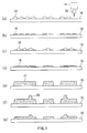
- Fig. 1 shows processes from an ink repellent treatment process to an interlayer post formation process.
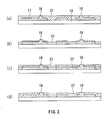
- Fig. 2 shows interlayer insulation film formation processes.
- Fig. 3 shows processes after the second wiring pattern formation.
- a multilayered printed wiring is formed on one side of the board 10.
- a conductive ink that is a liquid discharged from a liquid drop discharge apparatus for use in the formation of the multilayered printed wiring.
- a gold particulate dispersion (made by Vacuum Metallurgical Co., Ltd. under the trade designation of "Perfect Gold") in which gold particulates having a diameter of about 10 nm are dispersed in toluene is diluted with toluene to have a viscosity of 3 [mPa ⁇ s].
- the liquid is used as the conductive ink in this embodiment.
- an ink repellent treatment water repellent treatment
- a position of the conductive ink discharged onto the board can be controlled with high accuracy.
- the board 10 comprising polyimide is cleaned with IPA, irradiated with an ultraviolet ray with a wavelength of 254 nm at intensity of 10 mW/cm 2 for 10 minutes, and then cleaned (ultraviolet ray irradiation cleaning).
- 0.1 g of hexadecafuluoro 1,1,2,2 tetrahydrodecyl triethoxysilane and the board 10 are fed into a closed container having a volume of 10 liter, and are held at 120 Celsius degree for 2 hours.
- An ink repellent monomolecular film is formed on the board 10.
- a contact angle between the surface of the board 10 on which the monomolecular film is formed and the conductive ink discharged thereon will be, for example, about 70 degree.
- the board 10 is irradiated with the ultraviolet ray having the same wavelength (254 nm) used in the cleaning for 2 minutes. As a result, the contact angle between the conductive ink and the surface of the board becomes about 35°.
- a receptor layer may be formed instead of the ink repellent treatment.
- the conductive ink is discharged onto the board 10 that is subjected to the ink repellent treatment.
- the ink is discharged from an ink jet head 11 of the liquid drop discharge apparatus as a liquid drop 12 to provide a bit map pattern having predetermined dot spaces. Then, a heat treatment is performed to form a conductive film pattern.
- the ink jet head 11 a head for commercially available printer (trade designation of "PM950C") is, for example, used. Since an ink inlet part is made of plastic, the ink inlet part is changed from plastic to metal jig so that the inlet part is not dissolved in an organic solvent.
- the conductive ink is discharged with a driving voltage of 20 V of the ink jet head 11, the liquid drop having a volume of 5 pico liter is discharged.
- the diameter of the liquid drop 12 is about 27 ⁇ m. After the liquid drop 12 is fallen down to the board 10 (at the contact angle of 35 degree), the liquid drop 12 is broaden on the board 10 to have a diameter of about 45 ⁇ m.
- a wiring pattern drawn on the board 10 is formed by designing white and black binary bit maps onto square grids having each side of 50 ⁇ m, and discharging the liquid drops 12 in accordance with the bit maps. As shown in Fig. 1(a), the conductive ink containing the gold particulates is discharged from the ink jet head 11 to the board 10 so that the ink is disposed per 50 ⁇ m.
- one liquid drop 13 fallen onto the board 10 broadens with a diameter of about 45 ⁇ m, the liquid drop 13 is not contacted with other liquid drop 13, and all dots (liquid drops 13) are disposed separately on the board 10.
- hot air of 100 Celsius degree is applied to the board 10 for 15 seconds to dry the conductive ink. Then, the board 10 is self-cooled for several minutes until it returns back to room temperature, resulting in the state shown in Fig. 1(b).
- Ink liquid drops 14 are formed such that the solvent is dried from the liquid drops 13 and have a thickness of about 2 ⁇ m.
- the ink liquid drops 14 have substantially the same ink repellency as those of the parts on the board having no ink liquid drops 14.
- liquid drops 15 containing the same liquid as the liquid drops 13 are discharged between the separated dots (ink liquid drops 14) under the same conditions.
- Fig. 1 shows only a sectional view. But, when the isolated dots or the ink liquid drops 14 exist also in a vertical direction thereof, the liquid drops 15 are also discharged between the dots.
- the discharge between the dots and the hot air drying are repeated 6 times in total including the above to form a wiring pattern 17 having a line width of 50 ⁇ m and a film thickness of 10 ⁇ m as shown in Fig. 1(e).
- the wiring pattern has no electrical conductivity.
- interlayer conductive posts (conductor posts) 18 for conducting with a second layer through an interlayer insulation film.
- the interlayer conductive posts can be formed by entirely the same processes as the first layer wiring formation processes as described above. In other words, the conductive ink containing silver particulates is discharged onto only places where interlayer conductivity is needed, is hot-air dried and is again discharged.
- the interlayer conductive posts 18 having a height of 10 ⁇ m from the first layer are formed by the discharges repeated 6 times in total as shown in Fig. 1(f).
- the board 10 patterned is heat treated at 300 Celsius degree in air for 30 minutes to electrically contact the silver particulates.
- the interlayer conductive posts 18 are formed integrally with the wiring patterns 17 of the first layer. By the heat treatment, a total thickness of the wiring patterns 17 and the interlayer conductive posts 18 becomes about half before the heat treatment as shown in Fig. 1(g).
- the silver wiring patterns have electrical conductivity of about 2 [ ⁇ cm].
- An adhesion between the wiring patterns 17 and the board 10 is evaluated by a Cellotape (registered trademark) test, resulting in sufficient adhesion without peeling.
- the board 10 on which the first layer wiring pattern 17 is formed is irradiated with an ultraviolet ray having a wavelength of 256 nm at intensity of 10 [mW/cm 2 ] for 5 minutes as a pretreatment. Inkphilicity is provided on the surface of the board 10 and the first wiring pattern.
- an ink 21 for forming the interlayer insulation film commercially available polyimide varnish (made by Du Pont Corp. under the trade designation of "Pile ML") is, for example, diluted with a solvent (N-methyl-2-pyrolidone) to adjust its viscosity to 20 [mPa ⁇ s].
- the ink 21 is applied to all portions excluding the interlayer conductive posts 18 using the same liquid drop discharge apparatus used in the formation of the conductive pattern in the aforementioned first layer wiring formation process.
- the amount of the ink liquid drops is, for example, 5 pico liter.
- the ink 21 is fallen down to and wets the surface of the inkphilic board 10 and the inkphilic wiring pattern 17. All portions excluding the interlayer conductive posts are covered with the ink 21.
- the surface of the ink 21 becomes flat by the self-leveling effect. As shown in Fig. 2(a), the ink 21 is re-applied several times by the liquid drop discharge apparatus so that the height of each interlayer conductive post 18 slightly protruded (about 0.1 ⁇ m) from the surface of the ink 21.
- the board 10 is heat-treated at 400 Celsius degree for 30 minutes to remove the solvent and to cure the polyimide.
- the thickness of the polyimide 22 becomes about half of that of the ink 21 before the heat treatment.
- the ink 21 is patterned and applied to the polyimide 22 as described above, so that each of interlayer conductive post 18 is slightly protruded from the surface of the ink 21, as shown in Fig. 2(c). Then, the board 10 is heat-treated at 400 Celsius degree for 30 minutes to cure the polyimide. As shown in Fig. 2(d), the thinnest thickness of the polyimide 22 is, for example, 8 ⁇ m in total.
- the surface of the polyimide 22 has irregularity based on the first wiring pattern.
- the ink is applied and fired so that a top surface of each post is slightly protruded
- the polyimide precursor may be applied not to entire surface, but to concave parts and be fired.
- the surface is flatten in the figures for simplicity.
- the interlayer insulation film (polyimide 22) can be formed to assure the exposure of the top surface of each interlayer conductive post 18.
- a second wiring pattern 31 is formed on the interlayer insulation film (polyimide 22) by the same process as the first layer.
- respective processes including the IPA cleaning, the ultraviolet ray irradiation cleaning, the ink repellency application by alkyl silane fluoride, the control of the contact angle by the ultraviolet ray irradiation, the pattern discharge of the ink containing the silver particulates, and the hot-air drying are performed. Then, the steps of the discharge, the hot-air drying, the discharge and the hot-air drying are repeated at required times.
- the interlayer conductive post 32 is formed using the similar process as the first layer, and then the board is fired together with the second wiring to be conductive.
- an interlayer insulation film 33 disposed between the second and third layers is formed using the similar process for forming the interlayer insulation film (polyimide 22) between the first and the second layers. Repeating the process the required number of times can make any required layers.
- Fig. 3(c) shows the board on which a third layer is formed.
- Fig. 4 is a process drawing showing the method of producing the multilayered wiring board according to a second embodiment of the present invention.
- multilayered printed wiring is formed on both sides of a core board 40.
- wiring pattern and the insulation film pattern are layered by the liquid drop discharge system similar to the first embodiment, wiring can be produced only on a single side of the board.
- normal double sided wiring board is used as the central core board 40. Starting with such board, similar processes as the first embodiment may be conducted on the both sides.
- the core substrate 40 may have no through-holes.
- the through-holes may be filled with a metal paste 41, non-through-holes are perforated to a copper foil of a board having a copper foil side and are filled with the metal paste. Perforation is generally made by photolithography or a laser irradiation.
- the though-holes or the non-through-holes may be filled with the conductive ink containing the silver particulates used in the first embodiment by the liquid drop discharge system.
- Fig. 5 is a process drawing showing the method of producing the multilayered wiring board according to a third embodiment of the present invention.
- re-wiring is formed by a Chip Scale Package (CSP) method, i.e., a wiring pattern is drawn directly on a chip to form the multilayered printed wiring.
- CSP Chip Scale Package
- an IC chip 50 on which aluminum pads 51 are formed is subjected to the ink repellent treatment using a monomolecular film as shown in Fig. 5(a).
- This ink repellent treatment is the same as in the first embodiment except that decyltriethoxysilane is used as a material of the monomolecular film.
- interlayer conductive posts 52 having a height of 5 ⁇ m and a diameter of 50 ⁇ m are formed in respective centers of the aluminum pads 51 by the similar processes as in the first embodiment. Furthermore, an interlayer insulation film 53 is formed up to the top surfaces of the interlayer conductive posts 52 by the similar processes as in the first embodiment. The interlayer insulation film 53 having a flat top surface can be formed, while exposing the top surfaces of the interlayer conductive posts 52 with certainty.
- Fig. 6 is a process drawing showing the method of producing the multilayered wiring board according to a fourth embodiment of the present invention.
- a coil shape at an antenna termination of a radio IC card 60 is formed by the production method in the above embodiments.
- Figs. 6(a'), (b') and (c') are sectional views between two pads 65 in Figs. 6(a), (b) and (c).
- the radio IC card 60 comprises an IC chip 63 and a coil shaped antenna 62 that are mounted on a polyimide film 61.
- the IC chip 63 comprises a nonvolatile memory, a logic circuit, a high frequency circuit and the like, and activates by catching at the antenna 62 radio waves transmitted from an external transmitter and receiving electric power supply.
- the IC chip 63 analyzes an signal received by the antenna 62, and allows the antenna 62 to issue a required signal based on an analyzed result.
- the coil shaped antenna 62 is formed on the polyimide film 61 as shown in Fig. 6(a) in the similar manner for forming the first wiring in the first embodiment.
- An termination 63a for mounting pad parts 64 and the IC chip 63 are formed concurrently with the antenna 62.
- interlayer conductor posts 65 are formed on the pad parts 64 in the similar manner as in the first embodiment.
- polyimide is applied in a pattern so that top surfaces of the interlayer conductive posts 65 are exposed, whereby an interlayer insulation film 66 is formed in the similar manner in the first embodiment.
- an conductive ink containing silver particulates is applied in a pattern shown in Fig. 6(c) by the liquid drop discharge system, and is fired to form wiring 67 for connecting both terminals of the coil shaped antenna 62 in the similar manner in the first embodiment.
- the IC chip 63 is mounted on a position shown in Fig. 6(c) using an anisotropic conductive film.
- a protective film (not shown) is laminated over the whole structure to provide the radio IC card 60.
- the radio IC card 60 can, for example, communicate with an external reader/writer 5 cm apart.
- the multilayered printed wiring can be provided by forming the interlayer conductive posts 65 to leave an area required for conducting the layers, even if the interlayer conductive posts 65 are not formed in advance.
- the interlayer insulation films 66 have tapered ends. Therefore, the wiring 67 can be formed on the interlayer insulation layer 66 by the liquid drop discharge system without disconnection.
- Fig. 7 is a perspective view showing an example of an mobile phone.
- a numeral 1000 designates a mobile phone body
- a numeral 1001 designates a display using the multilayered wiring board produced by the method in the above-mentioned embodiments.
- Fig. 8 is a perspective view showing an example of an electronic watch.
- a numeral 1100 designates a watch body
- a numeral 1101 designates a display using the multilayered wiring board produced by the method in the above-mentioned embodiments.
- Fig. 9 is a perspective view showing an example of an mobile information processing apparatus.
- a numeral 1200 designates an information processing apparatus
- a numeral 1202 designates an input part such as a keyboard
- a numeral 1204 designates an information processing apparatus body
- a numeral 1206 designates a display using the multilayered wiring board produced by the method in the above-mentioned embodiments.
- the electronic apparatuses shown in Figs. 7 to 9 comprise the multilayered wiring board produced by the method in the above-mentioned embodiments, and therefore are produced in simple production processes with a shortened production time than ever.
- the production method according to the present invention can be applied to not only the multilayered printed wiring, but also a multilayered wiring for large scale display devices.
- the interlayer insulation film is disposed around the conductor posts using the liquid drop discharge system, whereby an elaborate multilayered wiring can be formed with relatively simple production processes.
Landscapes
- Engineering & Computer Science (AREA)
- Manufacturing & Machinery (AREA)
- Microelectronics & Electronic Packaging (AREA)
- Production Of Multi-Layered Print Wiring Board (AREA)
- Manufacturing Of Printed Wiring (AREA)
Abstract
Description
Claims (26)
- A method of producing a multilayered wiring board having at least two wiring layers, an interlayer insulation film between the wiring layers, and a conductor post for conducting between the wiring layers,
wherein the interlayer insulation film is disposed around the conductor post using a liquid drop discharge system. - A method of producing a multilayered wiring board according to Claim 1, wherein the interlayer insulation film is formed using a liquid with a low viscosity.
- A method of producing a multilayered wiring board according to Claim 1 or 2, wherein the conductor post is formed by the liquid drop discharge system.
- A method of producing a multilayered wiring board according to any one of Claims 1 to 3, wherein at least one of the wiring layers is formed by the liquid drop discharge system.
- A method of producing a multilayered wiring board according to Claim 1, wherein all of the interlayer insulation film, the wiring layers and the conductor post are formed by the liquid drop discharge system.
- A method of producing a multilayered wiring board according to Claim 1, wherein all of the interlayer insulation film, the wiring layers and the conductor post are formed using the same liquid drop discharge apparatus.
- A method of producing a multilayered wiring board according to any one of Claims 3 to 6, the wiring and the conductor post are formed by repeating a discharge of a conductive ink to a board and a drying of the conductive ink discharged alternately.
- A method of producing a multilayered wiring board according to any one of Claims 1 to 7, wherein a discharged surface of the board is subjected a water repellent treatment before a liquid drop is discharged onto the board by the liquid drop discharge system.
- A method of producing a multilayered wiring board according to any one of Claims 1 to 7, wherein a receptor layer is formed on a discharged surface of the board before the liquid drop is discharged onto the board by the liquid drop discharge system.
- A method of producing a multilayered wiring board according to any one of Claims 1 to 9, wherein the wiring and the conductor post are formed by firing the conductive ink that is discharged onto the board and is dried.
- A method of producing a multilayered wiring board according to any one of Claims 1 to 10, wherein the step of forming the interlayer insulation comprising the step of discharging a liquid containing polyimide or a polyimide precursor onto the board.
- A method of producing a multilayered wiring board according to Claim 11, wherein the step of forming the interlayer insulation film comprises the step of firing the board after the liquid containing polyimide or polyimide precursor is discharged onto the board.
- A method of producing a multilayered wiring board according to Claim 10, wherein an amount of a liquid drop discharged by the liquid drop discharge system, a density of the liquid drop disposed and a time for scanning the discharge are adjusted so that the interlayer insulation layer has substantially the same height as that of the conductor post.
- A method of producing a multilayered wiring board, comprising the steps of:forming the interlayer insulation film and the conductor post so that the interlayer insulation layer has substantially the same height as that of the conductor post, and forming at least one of the wiring layer, the interlayer insulation layer and the conductor post on the interlayer insulation film or the conductor post using the method of producing the multilayered wiring board according to any one of Claims 1 to 13.
- A method of producing a multilayered wiring board, comprising the step of forming the multilayered wiring on a chip having an integrated circuit using the method of producing the multilayered wiring board according to any one of Claims 1 to 14.
- A method of producing a multilayered wiring board, comprising the step of using the method of producing the multilayered wiring board according to any one of Claims 1 to 14 to the board on which at least one of the wiring layer, the interlayer insulation layer and the conductor post is formed by the production method other than the production method according to any one of claims 1 to 14.
- A method of producing a multilayered wiring layer board comprising at least two wiring layers, an interlayer insulation film disposed between the wiring layers, and a conductor post for conducting between the wiring layers,
wherein at least one of the wiring layer, the interlayer insulation layer and the conductor post is produced by the method of producing the multilayered wiring board according to any one of Claims 1 to 16. - A multilayered wiring board, comprising at least two wiring layers, an interlayer insulation film disposed between the wiring layers, and a conductor post for conducting between the wiring layers,
wherein the conductor post has a shape like a bowl turned upside down with a thickness of 1 micrometer to 20 micrometer and a diameter of 10 micrometer to 200 micrometer. - A multilayered wiring board according to Claim 18, wherein the interlayer insulation layer has substantially the same height as that of the conductor post.
- A multilayered wiring board according to Claim 18 or 19, wherein a top surface of the interlayer insulation film is formed substantially flat.
- An electronic device comprising a wiring layer, an interlayer insulation film formed on the wiring layer, and a conductor post connected to wiring of the wiring layer and formed through the interlayer insulation film,
wherein at least one of the wiring layer, the interlayer insulation layer and the conductor post is produced by the production method according to any one of Claims 1 to 16. - An electronic device comprising a wiring layer, an interlayer insulation film formed on the wiring layer, and a conductor post connected to wiring of the wiring layer and formed through the interlayer insulation film,
wherein the conductor post has a shape like a bowl turned upside down with a thickness of 1 micrometer to 20 micrometer and a diameter of 10 micrometer to 200 micrometer. - An electronic device according to Claim 22, wherein the interlayer insulation layer has substantially the same height as that of the conductor post.
- An electronic device according to Claim 22 or 23,
wherein a top surface of the interlayer insulation film is formed substantially flat. - An electronic apparatus comprising the multilayered wiring board according to any one of Claims 17 to 20.
- An electronic apparatus comprising the electronic device according to any one of Claims 21 to 24.
Applications Claiming Priority (2)
| Application Number | Priority Date | Filing Date | Title |
|---|---|---|---|
| JP2002113621A JP3925283B2 (en) | 2002-04-16 | 2002-04-16 | Method for manufacturing electronic device, method for manufacturing electronic device |
| JP2002113621 | 2002-04-16 |
Publications (2)
| Publication Number | Publication Date |
|---|---|
| EP1355522A2 true EP1355522A2 (en) | 2003-10-22 |
| EP1355522A3 EP1355522A3 (en) | 2004-11-10 |
Family
ID=28672616
Family Applications (1)
| Application Number | Title | Priority Date | Filing Date |
|---|---|---|---|
| EP03252346A Withdrawn EP1355522A3 (en) | 2002-04-16 | 2003-04-14 | Multilayered wiring board, method of producing multilayered wiring board, electronic device and electronic apparatus |
Country Status (4)
| Country | Link |
|---|---|
| US (1) | US7285305B2 (en) |
| EP (1) | EP1355522A3 (en) |
| JP (1) | JP3925283B2 (en) |
| CN (1) | CN1284431C (en) |
Cited By (4)
| Publication number | Priority date | Publication date | Assignee | Title |
|---|---|---|---|---|
| WO2007140477A3 (en) * | 2006-05-31 | 2008-03-13 | Cabot Corp | Polyimide insulative layers in multi-layered printed electronic features |
| US7598129B2 (en) | 2003-11-14 | 2009-10-06 | Semiconductor Energy Laboratory Co., Ltd. | Light-emitting device and method for manufacturing the same |
| US8053780B2 (en) | 2003-11-14 | 2011-11-08 | Semiconductor Energy Laboratory Co., Ltd. | Semiconductor element, method for manufacturing the same, liquid crystal display device, and method for manufacturing the same |
| FR3147480A1 (en) * | 2023-04-03 | 2024-10-04 | Ico Novation | Process for manufacturing a printed circuit board |
Families Citing this family (57)
| Publication number | Priority date | Publication date | Assignee | Title |
|---|---|---|---|---|
| DE10256662A1 (en) * | 2002-12-04 | 2004-06-17 | Robert Bosch Gmbh | Fuel injector |
| KR100484168B1 (en) * | 2002-10-11 | 2005-04-19 | 삼성전자주식회사 | Ink jet printhead and manufacturing method thereof |
| JP2004337701A (en) * | 2003-05-14 | 2004-12-02 | Seiko Epson Corp | Droplet discharging method and droplet discharging device |
| US20070123027A1 (en) * | 2003-12-22 | 2007-05-31 | Michinori Shinkai | Wiring forming method, wiring forming apparatus, and wiring board |
| JP4281584B2 (en) | 2004-03-04 | 2009-06-17 | セイコーエプソン株式会社 | Manufacturing method of semiconductor device |
| JP2005268543A (en) * | 2004-03-18 | 2005-09-29 | Hitachi Chem Co Ltd | Insulating layer and material for forming the same |
| DE602005022874D1 (en) * | 2004-06-03 | 2010-09-23 | Molecular Imprints Inc | FLUID AND DROP EXPOSURE AS REQUIRED FOR MANUFACTURE IN THE NANO AREA |
| JP4193758B2 (en) * | 2004-06-18 | 2008-12-10 | セイコーエプソン株式会社 | Layer forming device |
| US20060033793A1 (en) * | 2004-08-10 | 2006-02-16 | Webster Grant A | Coupling agent patterning |
| JP4683180B2 (en) * | 2004-08-19 | 2011-05-11 | セイコーエプソン株式会社 | Wiring board manufacturing method and multilayer wiring board manufacturing method |
| JP4506809B2 (en) * | 2004-08-20 | 2010-07-21 | セイコーエプソン株式会社 | MULTILAYER STRUCTURE FORMING METHOD, WIRING BOARD AND ELECTRONIC DEVICE MANUFACTURING METHOD |
| JP4052295B2 (en) * | 2004-08-25 | 2008-02-27 | セイコーエプソン株式会社 | MULTILAYER WIRING BOARD MANUFACTURING METHOD, ELECTRONIC DEVICE, AND ELECTRONIC DEVICE |
| JP4100385B2 (en) | 2004-09-22 | 2008-06-11 | セイコーエプソン株式会社 | Multilayer structure forming method, wiring board manufacturing method, and electronic device manufacturing method |
| JP2006100401A (en) | 2004-09-28 | 2006-04-13 | Seiko Epson Corp | Wiring pattern forming method, wiring pattern, electronic device |
| JP2006156943A (en) | 2004-09-28 | 2006-06-15 | Seiko Epson Corp | Wiring pattern forming method, wiring pattern, and electronic device |
| CN100415518C (en) * | 2004-09-28 | 2008-09-03 | 精工爱普生株式会社 | Forming method of wiring pattern |
| JP3928638B2 (en) | 2004-09-28 | 2007-06-13 | セイコーエプソン株式会社 | Wiring board manufacturing method and electronic device |
| JP4506384B2 (en) * | 2004-09-28 | 2010-07-21 | セイコーエプソン株式会社 | PATTERN FORMING METHOD, WIRING BOARD MANUFACTURING METHOD, AND ELECTRONIC DEVICE |
| JP4297106B2 (en) * | 2005-02-23 | 2009-07-15 | セイコーエプソン株式会社 | Film pattern forming method, device manufacturing method, electro-optical device, and electronic apparatus |
| EP1859662B1 (en) | 2005-03-14 | 2015-08-05 | Ricoh Company, Ltd. | Method of manufacturing a multilayer wiring structure |
| JP4293181B2 (en) | 2005-03-18 | 2009-07-08 | セイコーエプソン株式会社 | Metal particle dispersion, method for producing metal particle dispersion, method for producing conductive film-formed substrate, electronic device and electronic apparatus |
| JP2006332094A (en) | 2005-05-23 | 2006-12-07 | Seiko Epson Corp | Method for manufacturing electronic substrate, method for manufacturing semiconductor device, and method for manufacturing electronic device |
| US8147903B2 (en) | 2005-06-22 | 2012-04-03 | Canon Kabushiki Kaisha | Circuit pattern forming method, circuit pattern forming device and printed circuit board |
| US7829135B2 (en) * | 2005-06-22 | 2010-11-09 | Canon Kabushiki Kaisha | Method and apparatus for forming multi-layered circuit pattern |
| JP4379386B2 (en) * | 2005-06-23 | 2009-12-09 | セイコーエプソン株式会社 | Multilayer structure forming method |
| JP4742715B2 (en) * | 2005-07-19 | 2011-08-10 | セイコーエプソン株式会社 | Wiring pattern forming method and wiring board manufacturing method |
| JP2007088004A (en) * | 2005-09-20 | 2007-04-05 | Seiko Epson Corp | Multilayer circuit board manufacturing method, multilayer circuit board, electro-optical device, and electronic apparatus |
| JP5021216B2 (en) * | 2006-02-22 | 2012-09-05 | イビデン株式会社 | Printed wiring board and manufacturing method thereof |
| US20070248798A1 (en) * | 2006-04-19 | 2007-10-25 | Canon Kabushiki Kaisha | Circuit board manufacturing process, circuit board manufactured by the process, and circuit board manufacturing apparatus |
| JP2008066576A (en) * | 2006-09-08 | 2008-03-21 | Seiko Epson Corp | Method of manufacturing circuit board |
| US20080119011A1 (en) * | 2006-11-20 | 2008-05-22 | Industrial Technology Research Institute | Method of film coating and device manufactured thereby |
| JPWO2008069055A1 (en) * | 2006-11-28 | 2010-03-18 | 京セラ株式会社 | Wiring board and semiconductor device mounting structure using the same |
| KR100871034B1 (en) * | 2007-06-12 | 2008-11-27 | 삼성전기주식회사 | Paste bump formation method of printed circuit board |
| TWI360205B (en) | 2007-06-20 | 2012-03-11 | Princo Corp | Multi-layer substrate and manufacture method there |
| WO2009006761A1 (en) * | 2007-07-12 | 2009-01-15 | Princo Corp. | Multi-layer baseboard and manufacturing method thereof |
| KR101044103B1 (en) * | 2008-04-03 | 2011-06-28 | 삼성전기주식회사 | Multilayer printed circuit board and its manufacturing method |
| KR100969437B1 (en) * | 2008-06-13 | 2010-07-14 | 삼성전기주식회사 | Printed circuit board and manufacturing method thereof |
| GB2462290B (en) * | 2008-07-31 | 2011-02-23 | Novalia Ltd | Printed article |
| JP2010087208A (en) * | 2008-09-30 | 2010-04-15 | Fujifilm Corp | Method for forming three-dimensional structure, method for manufacturing semiconductor device, and semiconductor device |
| JP2011134879A (en) * | 2009-12-24 | 2011-07-07 | Seiko Epson Corp | Method for producing build-up substrate |
| US8476538B2 (en) * | 2010-03-08 | 2013-07-02 | Formfactor, Inc. | Wiring substrate with customization layers |
| KR20110113980A (en) * | 2010-04-12 | 2011-10-19 | 삼성전자주식회사 | Multilayer printed circuit board including film and manufacturing method thereof |
| JP5541017B2 (en) * | 2010-09-08 | 2014-07-09 | 日立化成株式会社 | Insulating layer forming material and insulating layer |
| US8617926B2 (en) * | 2010-09-09 | 2013-12-31 | Advanced Micro Devices, Inc. | Semiconductor chip device with polymeric filler trench |
| JP5849489B2 (en) * | 2011-07-21 | 2016-01-27 | セイコーエプソン株式会社 | Electro-optical device, projection display device, electronic apparatus, and method of manufacturing electro-optical device |
| JP5670372B2 (en) * | 2012-03-29 | 2015-02-18 | 富士フイルム株式会社 | Liquid ejection apparatus and control method thereof |
| FR3000598B1 (en) * | 2012-12-27 | 2016-05-06 | Commissariat Energie Atomique | IMPROVED METHOD FOR PRODUCING A CONTACT RESUME STRUCTURE |
| WO2014194049A1 (en) * | 2013-05-31 | 2014-12-04 | The Regents Of The University Of California | Through silicon vias and thermocompression bonding using inkjet-printed nanoparticles |
| JP6370077B2 (en) * | 2014-03-25 | 2018-08-08 | 株式会社Fuji | Electronic device manufacturing method and manufacturing apparatus |
| US9357640B2 (en) | 2014-09-22 | 2016-05-31 | Oce'-Technologies B.V. | Method of manufacturing a multi-layer printed circuit board |
| US11284521B2 (en) * | 2015-06-30 | 2022-03-22 | 3M Innovative Properties, Company | Electronic devices comprising a via and methods of forming such electronic devices |
| EP3352537B1 (en) * | 2015-09-18 | 2024-03-27 | Konica Minolta, Inc. | Wiring laminated structural body forming method |
| US10257930B2 (en) * | 2016-06-22 | 2019-04-09 | R&D Circuits, Inc. | Trace anywhere interconnect |
| CN109428007B (en) * | 2017-08-29 | 2020-06-26 | 京东方科技集团股份有限公司 | Method for preparing a display substrate, display substrate and display device |
| EP3989275A4 (en) * | 2019-06-18 | 2022-07-13 | Fuji Corporation | PRINTED CIRCUIT BOARD FABRICATION METHOD AND PRINTED CIRCUIT BOARD FABRICATION DEVICE |
| US12048102B2 (en) * | 2019-07-30 | 2024-07-23 | Fuji Corporation | Electronic circuit production method using 3D layer shaping |
| WO2022049994A1 (en) | 2020-09-03 | 2022-03-10 | コニカミノルタ株式会社 | Method of pattern formation |
Family Cites Families (26)
| Publication number | Priority date | Publication date | Assignee | Title |
|---|---|---|---|---|
| US4668533A (en) * | 1985-05-10 | 1987-05-26 | E. I. Du Pont De Nemours And Company | Ink jet printing of printed circuit boards |
| JPS63170994A (en) * | 1986-05-30 | 1988-07-14 | 古河電気工業株式会社 | Multilayer printed interconnection board and manufacture of the same |
| JPH0797602B2 (en) * | 1988-05-06 | 1995-10-18 | 日本電気株式会社 | Semiconductor integrated circuit device |
| FR2650472A1 (en) * | 1989-07-27 | 1991-02-01 | Bull Sa | METHOD FOR DEPOSITING AN INSULATING LAYER ON A CONDUCTIVE LAYER OF THE MULTI-LAYER NETWORK OF A HIGH DENSITY INTEGRATED CIRCUIT CONNECTION CARD, AND RESULTING CARD |
| US5948533A (en) * | 1990-02-09 | 1999-09-07 | Ormet Corporation | Vertically interconnected electronic assemblies and compositions useful therefor |
| JPH0710030B2 (en) * | 1990-05-18 | 1995-02-01 | インターナシヨナル・ビジネス・マシーンズ・コーポレーシヨン | Method for manufacturing multilayer wiring board |
| US6175422B1 (en) | 1991-01-31 | 2001-01-16 | Texas Instruments Incorporated | Method and apparatus for the computer-controlled manufacture of three-dimensional objects from computer data |
| US5594652A (en) * | 1991-01-31 | 1997-01-14 | Texas Instruments Incorporated | Method and apparatus for the computer-controlled manufacture of three-dimensional objects from computer data |
| JPH07231154A (en) | 1994-02-21 | 1995-08-29 | Matsushita Electric Works Ltd | Method of forming three-dimensional circuit |
| EP0805614B1 (en) * | 1995-11-17 | 2005-04-13 | Kabushiki Kaisha Toshiba | Multilayered wiring board, prefabricated material for multilayered wiring board, process of manufacturing multilayered wiring board, electronic parts package, and method for forming conductive pillar |
| US5650199A (en) * | 1995-11-22 | 1997-07-22 | Aem, Inc. | Method of making a multilayer electronic component with inter-layer conductor connection utilizing a conductive via forming ink |
| CN1153240C (en) * | 1997-03-21 | 2004-06-09 | 佳能株式会社 | Method for manufacturing printed substrate, electron emission element, electron source and image forming device |
| JPH1154928A (en) | 1997-06-03 | 1999-02-26 | Ngk Spark Plug Co Ltd | Wiring board and its manufacturing method |
| WO1999019900A2 (en) * | 1997-10-14 | 1999-04-22 | Patterning Technologies Limited | Method of forming an electronic device |
| JPH11163499A (en) | 1997-11-28 | 1999-06-18 | Nitto Boseki Co Ltd | Manufacturing method of printed wiring board and printed wiring board by this manufacturing method |
| US6487774B1 (en) * | 1998-01-22 | 2002-12-03 | Matsushita Electric Industrial Co., Ltd. | Method of forming an electronic component using ink |
| US6261941B1 (en) * | 1998-02-12 | 2001-07-17 | Georgia Tech Research Corp. | Method for manufacturing a multilayer wiring substrate |
| JP4741045B2 (en) | 1998-03-25 | 2011-08-03 | セイコーエプソン株式会社 | Electric circuit, manufacturing method thereof and electric circuit manufacturing apparatus |
| JPH11274681A (en) | 1998-03-25 | 1999-10-08 | Seiko Epson Corp | Electronic device and manufacturing method thereof |
| JP2000294930A (en) | 1999-04-06 | 2000-10-20 | Mitsubishi Electric Corp | Method of manufacturing multilayer printed board and semiconductor device using this multilayer printed board |
| JP2001267725A (en) * | 2000-03-16 | 2001-09-28 | Matsushita Electric Ind Co Ltd | Method of manufacturing ceramic thick film printed circuit board |
| JP2001267308A (en) | 2000-03-22 | 2001-09-28 | Seiko Epson Corp | Protective film forming apparatus and semiconductor manufacturing apparatus using the same |
| US6707153B2 (en) | 2000-03-23 | 2004-03-16 | Seiko Epson Corporation | Semiconductor chip with plural resin layers on a surface thereof and method of manufacturing same |
| US7442408B2 (en) * | 2002-03-26 | 2008-10-28 | Hewlett-Packard Development Company, L.P. | Methods for ink-jet printing circuitry |
| JP3801158B2 (en) * | 2002-11-19 | 2006-07-26 | セイコーエプソン株式会社 | MULTILAYER WIRING BOARD MANUFACTURING METHOD, MULTILAYER WIRING BOARD, ELECTRONIC DEVICE, AND ELECTRONIC DEVICE |
| US7202155B2 (en) * | 2003-08-15 | 2007-04-10 | Semiconductor Energy Laboratory Co., Ltd. | Method for manufacturing wiring and method for manufacturing semiconductor device |
-
2002
- 2002-04-16 JP JP2002113621A patent/JP3925283B2/en not_active Expired - Fee Related
-
2003
- 2003-04-14 EP EP03252346A patent/EP1355522A3/en not_active Withdrawn
- 2003-04-15 CN CNB031104312A patent/CN1284431C/en not_active Expired - Fee Related
- 2003-04-16 US US10/417,398 patent/US7285305B2/en not_active Expired - Fee Related
Cited By (6)
| Publication number | Priority date | Publication date | Assignee | Title |
|---|---|---|---|---|
| US7598129B2 (en) | 2003-11-14 | 2009-10-06 | Semiconductor Energy Laboratory Co., Ltd. | Light-emitting device and method for manufacturing the same |
| US8053780B2 (en) | 2003-11-14 | 2011-11-08 | Semiconductor Energy Laboratory Co., Ltd. | Semiconductor element, method for manufacturing the same, liquid crystal display device, and method for manufacturing the same |
| US8518728B2 (en) | 2003-11-14 | 2013-08-27 | Semiconductor Energy Laboratory Co., Ltd. | Semiconductor element, method for manufacturing the same, liquid crystal display device, and method for manufacturing the same |
| WO2007140477A3 (en) * | 2006-05-31 | 2008-03-13 | Cabot Corp | Polyimide insulative layers in multi-layered printed electronic features |
| FR3147480A1 (en) * | 2023-04-03 | 2024-10-04 | Ico Novation | Process for manufacturing a printed circuit board |
| WO2024208735A1 (en) * | 2023-04-03 | 2024-10-10 | Ico Novation | Method for manufacturing a printed circuit |
Also Published As
| Publication number | Publication date |
|---|---|
| CN1284431C (en) | 2006-11-08 |
| EP1355522A3 (en) | 2004-11-10 |
| US20040000429A1 (en) | 2004-01-01 |
| JP2003309369A (en) | 2003-10-31 |
| CN1452451A (en) | 2003-10-29 |
| US7285305B2 (en) | 2007-10-23 |
| JP3925283B2 (en) | 2007-06-06 |
Similar Documents
| Publication | Publication Date | Title |
|---|---|---|
| US7285305B2 (en) | Multilayered wiring board, method of producing multilayered wiring board, electronic device and electronic apparatus | |
| KR100572606B1 (en) | Multilayer circuit boards, manufacturing method thereof, electronic devices and electronic devices | |
| US6973710B2 (en) | Method and apparatus for making devices | |
| JP4291279B2 (en) | Flexible multilayer circuit board | |
| JP2002261048A (en) | Device manufacturing method and device manufacturing apparatus | |
| JP2004527814A (en) | Method for manufacturing a new cheap radio frequency identification device | |
| US20070014975A1 (en) | Method of manufacturing wiring substrate, and wiring substrate | |
| US7370410B2 (en) | Method of manufacturing a device, device, non-contact type card medium, and electronic equipment | |
| KR100704915B1 (en) | Printed Circuit Board with Fine Pattern and Manufacturing Method Thereof | |
| US5937494A (en) | Method for assembling an ink-jet pen having a double-sided electrical interconnect flexible circuit | |
| WO2000035260A1 (en) | Method of manufacturing ceramic substrate | |
| KR100769636B1 (en) | Multilayered structure forming method | |
| JP2003318542A (en) | Method of forming multilayer wiring, multilayer wiring board, device, method of manufacturing device, and electronic equipment | |
| US6660941B2 (en) | Electronic parts mounting board and production method thereof | |
| JP2007116193A (en) | Multilayer wiring board manufacturing method, electronic device, electronic equipment | |
| JP2001284801A (en) | Method of manufacturing multilayer printed board | |
| US7728234B2 (en) | Coreless thin substrate with embedded circuits in dielectric layers and method for manufacturing the same | |
| JP4049146B2 (en) | Element manufacturing method and element manufacturing apparatus | |
| JPH08307057A (en) | Multilayer printed circuit board and manufacturing method thereof | |
| JP2005340437A (en) | MULTILAYER WIRING BOARD MANUFACTURING METHOD, ELECTRONIC DEVICE, AND ELECTRONIC DEVICE | |
| JP2006179953A (en) | Multilayer wiring board, electronic device and electronic equipment | |
| US20030215566A1 (en) | Fine patterning and fine solid via process for multi-layer substrate | |
| JP2005183847A (en) | Method for forming wiring board | |
| JP2005167048A (en) | Multilayer wiring board | |
| JP2003069226A (en) | Semiconductor device substrate and method of manufacturing the same |
Legal Events
| Date | Code | Title | Description |
|---|---|---|---|
| PUAI | Public reference made under article 153(3) epc to a published international application that has entered the european phase |
Free format text: ORIGINAL CODE: 0009012 |
|
| AK | Designated contracting states |
Kind code of ref document: A2 Designated state(s): AT BE BG CH CY CZ DE DK EE ES FI FR GB GR HU IE IT LI LU MC NL PT RO SE SI SK TR |
|
| AX | Request for extension of the european patent |
Extension state: AL LT LV MK |
|
| PUAL | Search report despatched |
Free format text: ORIGINAL CODE: 0009013 |
|
| AK | Designated contracting states |
Kind code of ref document: A3 Designated state(s): AT BE BG CH CY CZ DE DK EE ES FI FR GB GR HU IE IT LI LU MC NL PT RO SE SI SK TR |
|
| AX | Request for extension of the european patent |
Extension state: AL LT LV MK |
|
| 17P | Request for examination filed |
Effective date: 20050413 |
|
| AKX | Designation fees paid |
Designated state(s): DE FR GB |
|
| 17Q | First examination report despatched |
Effective date: 20090407 |
|
| STAA | Information on the status of an ep patent application or granted ep patent |
Free format text: STATUS: THE APPLICATION IS DEEMED TO BE WITHDRAWN |
|
| 18D | Application deemed to be withdrawn |
Effective date: 20101103 |