EP1353381A1 - Matrice de photodetecteurs, à pixels isolés et grillé de stockage, hybridee sur un circuit de lecture - Google Patents
Matrice de photodetecteurs, à pixels isolés et grillé de stockage, hybridee sur un circuit de lecture Download PDFInfo
- Publication number
- EP1353381A1 EP1353381A1 EP03100971A EP03100971A EP1353381A1 EP 1353381 A1 EP1353381 A1 EP 1353381A1 EP 03100971 A EP03100971 A EP 03100971A EP 03100971 A EP03100971 A EP 03100971A EP 1353381 A1 EP1353381 A1 EP 1353381A1
- Authority
- EP
- European Patent Office
- Prior art keywords
- walls
- doped
- face
- photodetector
- array according
- Prior art date
- Legal status (The legal status is an assumption and is not a legal conclusion. Google has not performed a legal analysis and makes no representation as to the accuracy of the status listed.)
- Granted
Links
Images



Classifications
-
- H—ELECTRICITY
- H10—SEMICONDUCTOR DEVICES; ELECTRIC SOLID-STATE DEVICES NOT OTHERWISE PROVIDED FOR
- H10F—INORGANIC SEMICONDUCTOR DEVICES SENSITIVE TO INFRARED RADIATION, LIGHT, ELECTROMAGNETIC RADIATION OF SHORTER WAVELENGTH OR CORPUSCULAR RADIATION
- H10F77/00—Constructional details of devices covered by this subclass
- H10F77/93—Interconnections
-
- H—ELECTRICITY
- H10—SEMICONDUCTOR DEVICES; ELECTRIC SOLID-STATE DEVICES NOT OTHERWISE PROVIDED FOR
- H10F—INORGANIC SEMICONDUCTOR DEVICES SENSITIVE TO INFRARED RADIATION, LIGHT, ELECTROMAGNETIC RADIATION OF SHORTER WAVELENGTH OR CORPUSCULAR RADIATION
- H10F39/00—Integrated devices, or assemblies of multiple devices, comprising at least one element covered by group H10F30/00, e.g. radiation detectors comprising photodiode arrays
- H10F39/80—Constructional details of image sensors
- H10F39/802—Geometry or disposition of elements in pixels, e.g. address-lines or gate electrodes
-
- H—ELECTRICITY
- H10—SEMICONDUCTOR DEVICES; ELECTRIC SOLID-STATE DEVICES NOT OTHERWISE PROVIDED FOR
- H10F—INORGANIC SEMICONDUCTOR DEVICES SENSITIVE TO INFRARED RADIATION, LIGHT, ELECTROMAGNETIC RADIATION OF SHORTER WAVELENGTH OR CORPUSCULAR RADIATION
- H10F39/00—Integrated devices, or assemblies of multiple devices, comprising at least one element covered by group H10F30/00, e.g. radiation detectors comprising photodiode arrays
- H10F39/80—Constructional details of image sensors
- H10F39/809—Constructional details of image sensors of hybrid image sensors
-
- H—ELECTRICITY
- H10—SEMICONDUCTOR DEVICES; ELECTRIC SOLID-STATE DEVICES NOT OTHERWISE PROVIDED FOR
- H10F—INORGANIC SEMICONDUCTOR DEVICES SENSITIVE TO INFRARED RADIATION, LIGHT, ELECTROMAGNETIC RADIATION OF SHORTER WAVELENGTH OR CORPUSCULAR RADIATION
- H10F39/00—Integrated devices, or assemblies of multiple devices, comprising at least one element covered by group H10F30/00, e.g. radiation detectors comprising photodiode arrays
- H10F39/80—Constructional details of image sensors
- H10F39/811—Interconnections
-
- H—ELECTRICITY
- H10—SEMICONDUCTOR DEVICES; ELECTRIC SOLID-STATE DEVICES NOT OTHERWISE PROVIDED FOR
- H10W—GENERIC PACKAGES, INTERCONNECTIONS, CONNECTORS OR OTHER CONSTRUCTIONAL DETAILS OF DEVICES COVERED BY CLASS H10
- H10W72/00—Interconnections or connectors in packages
- H10W72/20—Bump connectors, e.g. solder bumps or copper pillars; Dummy bumps; Thermal bumps
-
- H—ELECTRICITY
- H10—SEMICONDUCTOR DEVICES; ELECTRIC SOLID-STATE DEVICES NOT OTHERWISE PROVIDED FOR
- H10W—GENERIC PACKAGES, INTERCONNECTIONS, CONNECTORS OR OTHER CONSTRUCTIONAL DETAILS OF DEVICES COVERED BY CLASS H10
- H10W72/00—Interconnections or connectors in packages
- H10W72/90—Bond pads, in general
-
- H—ELECTRICITY
- H10—SEMICONDUCTOR DEVICES; ELECTRIC SOLID-STATE DEVICES NOT OTHERWISE PROVIDED FOR
- H10W—GENERIC PACKAGES, INTERCONNECTIONS, CONNECTORS OR OTHER CONSTRUCTIONAL DETAILS OF DEVICES COVERED BY CLASS H10
- H10W72/00—Interconnections or connectors in packages
- H10W72/90—Bond pads, in general
- H10W72/941—Dispositions of bond pads
- H10W72/9415—Dispositions of bond pads relative to the surface, e.g. recessed, protruding
Definitions
- the invention relates to a matrix of photodetectors, with isolated pixels and photogrid, hybridized on a read circuit.
- the detector arrays have the most often for the purpose of transcribing images. They can also be used for light signals from measuring devices. The light spectrum that they treat can go from infrared to ultraviolet. They deliver electrical signals in ratio with the luminous intensities received. Some deliver several signals in parallel, to transmit information more quickly, to separate the signals from filters different colors (therefore wavelengths).
- Some structures have sites photosensitive and signal amplifiers delivered by sites arranged side by side. of the charge storage grids (photogrids) can be used for these structures. By changing the potential of the grid, the charges are injected together towards the amplifiers.
- the invention proposes a structure comprising a matrix of photodetectors whose surface is entirely reserved for collecting the light and for which the detection works with a capacitive charge storage grid electric (called photogrid).
- photogrid capacitive charge storage grid electric
- Such a structure also has the distinction of separating electrically photodetectors through walls dielectric of the photogrid.
- We get a photodetection structure by hybridization of the array of photodetectors with grid and common base on an amplifier circuit.
- the subject of the invention is therefore a matrix of photodetectors intended to be hybridized on a reading circuit and constituted from a plate of semiconductor material having a receiving a light to be detected and an opposite face said hybridization face, characterized in that the plate is divided into pixels, each pixel constituting a photodetector, the pixels being separated from each other others by means of separation formed transversely in the plate and comprising a photogrid for photodetectors, each photodetector presenting, on the hybridization face, a connection pad for hybridizing the matrix from photodetectors to the read circuit.
- the means of separation include by walls comprising an electrically conductive wall taken sandwiched between electrically insulating walls, thus constituting with the semiconductor material the plate adjacent to the wall a photogrid of MOS type, each photodetector comprising a first zone doped and a second doped zone, the first zones doped ensuring electrical contact with the connection pads of the photodetectors, the second doped zones ensuring contact with a first common electrode, so-called common base electrode of the pixels, located on the hybridization face, the walls electrically conductors of the walls being connected to a second common electrode located on the hybridization face.
- the first electrode common and the second common electrode form interdigitated combs.
- the electrically conductive wall can be doped polysilicon and the walls electrically insulating walls can be oxide of silicon.
- the first doped areas are enough areas extended to reach the MOS photogrid.
- the means of separation include walls comprising an electrically conductive wall opening on the plate hybridization face and extending to inside the plate being covered with a layer of electrically insulating material up to a top not reaching the receiving face of a light, thus constituting with the material semiconductor of the plate adjacent to the wall a MOS photogrid, each photodetector comprising a first doped zone and a second zone doped, the first doped zones ensuring the catches electrical contact with the connection pads of the photodetectors, the second doped zones being located between the receiving face of a light and the top of the walls and ensuring contact electric with a first common electrode located on the receiving side of a light, the face of hybridization supporting a second common electrode electrically connecting the walls electrically conductive walls that open there.
- the matrix of photodetectors comprises connecting means electric through the plate of material semiconductor to connect the first electrode common to a conductive beach located on the face hybridization.
- the first electrode common includes electrical conductors possessing a shape to reflect light to detect to those parts of the receiving face which do not have electrical conductors.
- This form of drivers electric can be a point directed towards the light to detect.
- the second electrode common features parts facing the plate of suitable surface semiconductor material to help think about the material semiconductor a fraction of light to detect which crosses the plate of semiconductor material.
- the electrically conductive wall can be doped polysilicon and the layer of material electrically insulating can be silicon oxide.
- the first doped areas are enough areas extended to reach the MOS photogrid.
- the doped zones are multiple doping zones of different depth and identical or complementary type.
- walls including an electrically wall conductor are aligned in a first direction, insulating walls being aligned in a second direction that is transverse to the first direction, the electrically conductive walls constituting independent photogrid lines.
- Figure 1 is a sectional view cross-section of a hybridized photodetector matrix on a reading circuit, according to a first mode of embodiment of the invention.
- the matrix of photodetectors 10 is made from a plate of material semiconductor 11 divided into pixels or photodetectors 12 by walls arranged transversely to the plate 11 and in all its thickness.
- the walls comprise an electrically conductive wall 13 sandwiched between two walls electrically insulating wall 14 and 15.
- An insulating wall taken between semiconductor material and an electrically wall conductor forms a MOS capacitor.
- the thickness insulation is chosen as fine as possible while being enough not to snap under tension applied.
- Each pixel 12 has two doped zones to make the contact between the metal and the semiconductor and the collection of loads.
- the doped zone 16 ensures the contact with the connection pad 18 of the photodetector.
- the area doped 17 ensures the contact with the electrode 19 which is a common electrode for all photodetectors.
- the conductive walls 13 are connected electrically, side hybridization side, at a electrode 21 which is a common electrode for all the conductive walls of the walls.
- the matrix of photodetectors 10 is covered, on the face intended to receive a light to detect, an electrically insulating layer and transparent 22. She is covered, on her face hybridization, an electrically insulating layer 23 open locally to ensure the different electrical connections.
- Figure 1 also shows a circuit of reading 30 associated with the matrix of photodetectors 10.
- the reading circuit 30 is made on a substrate in silicon.
- amplifiers and CMOS 31 or bipolar or BiCMOS processing circuits were made on the substrate. For example, recognizes doping areas P or N 32 and 33, the polysilicon grids 34, drain contacts and source 35 and 36 and a silicon oxide layer engraved 37.
- Hybridization of the matrix of photodetectors 10 on the reading circuit 30 is done by means of fusible beads.
- the connection pads 18 photodetectors are connected to the reading circuit by balls 41.
- the common electrode 19 is connected to the reading circuit by balls 42.
- the electrode common 21 is connected to the read circuit by balls 43.
- Figure 2 is a top view of the Figure 1 according to section II-II. It allows to show the arrangement of the different electrodes and pads of connection on the hybridization face of the matrix of photodetectors. Note that the common electrode 21 and the common electrode 19 form combs interdigitated. The connection pads 18 form islets. The electrically conductive walls 13 of the walls were shown in phantom.
- Figure 3 is a sectional view cross-section of an alternative embodiment of a matrix of photodetectors on a read circuit, according to the first embodiment of the invention.
- the photodetector matrix is virtually identical to the one shown in Figure 1 with the exception of doped 16 which are the doped zones corresponding to the connection pads of the photodetectors. These areas doped 16 are such that, for each photodetector, the distance between each doped zone 16 and the zone of Storage of the capacitor charges is reduced. In fact, there is an extension of the doped zone 16 along the walls. There is a recovery zone of MOS capacitor and the doped zone 16 like this is typically done in MOS transistors.
- Figure 4 is a sectional view cross-section of a hybridized photodetector matrix on a reading circuit, according to a second mode of embodiment of the invention.
- the matrix of photodetectors 50 is made from a plate of material semiconductor 51 divided into pixels or photodetectors 52 by walls arranged transversely to the plate 51 and according to a part of its thickness.
- the walls include an electrically conductive wall 53 leading to the hybridization face of the plate 51 and covered with a layer of electrically isolator 54 extending on the hybridization face of the matrix of photodetectors.
- the top of the wall as well constituted leaves a zone of material semiconductor before the light receiving face of the plate 51. These walls form a MOS capacitor.
- Part 57 of semiconductor material between the insulating layer on the top walls and the face of the plate 51 intended to receive the light to be detected is doped and is in contact with an electrical conductor of a first electrode 59.
- the electrical separation of the pixels is so assured. Indeed, the doping of this part 57, in contact with the electrical conductor 59, connected to a reference potential, prohibits the passage of loads from one pixel to another.
- Each pixel 52 has at its center a doped zone 56 in a complementary manner with respect to the doped zone 57 and located on the hybridization face side of the matrix of photodetectors.
- the doped zones 56 are in electrical contact with the connection pads correspondent 58.
- the matrix of photodetectors 50 is covered, on its face intended to receive a light to detect, an electrically insulating layer 62 open locally to ensure the different electrical connections. She is covered, on her face hybridization, the extension of the layer electrically insulating 54 open locally for ensure the different electrical connections.
- the face of the photodetector matrix intended to receive the light to be detected therefore supports a first common electrode 59.
- the parts of this first common electrode 59 located to the left and to right of the figure are electrically connected to contact pads 69, located on the hybridization face of the matrix of photodetectors, by traverses conductive 79.
- the first common electrode 59 forms a narrow grid so that the semiconductor material of the matrix receives the maximum of light.
- the electrical conductors of this electrode are from preferably sharpened to point the light incident to the non-metallic parts of the face receiving light.
- the conductive walls 53 are connected electrically, side hybridization side, at a electrode 61 which constitutes the second electrode common.
- the electrode 61 covers the maximum area to think about the semiconductor material the light that would not have been absorbed.
- Figure 4 also shows a circuit of reading 30 associated with the matrix of photodetectors 50. It is similar to that of Figure 1.
- Hybridization of the matrix of photodetectors 50 on the reading circuit 30 is done by means of fusible beads.
- the connection pads 58 photodetectors are connected to the reading circuit by balls 71.
- the first common electrode 59 is connected to the reading circuit by balls 72 by through the conductive bushings 79 and contact pads 69.
- the second common electrode 61 is connected to the reading circuit by balls 73.
- Figure 5 is a sectional view cross-section of an alternative embodiment of a matrix of photodetectors on a read circuit, according to the second embodiment of the invention.
- the matrix of photodetectors is practically identical to that shown in Figure 4 at the exception of the doped areas 56 which are the zones doped corresponding to the connection pads of the photodetectors. Doped areas 56 have been expanded to join the capacitor. There exists a overlap zone between the doped zones 56 and the second common electrode 61.
- the reduction of the electric distance between the capacitor and the connection pad allows a better transfer of charges stored in the channel of the solar cell.
- the area of semiconductor material remaining between capacitor and the doped zone 56 allows the redistribution of charges stored throughout the pixel at the time of the permutation of the gate potential.
- deletion of this zone allows for a quick transition from loads directly from the grid to the connection pad at the time of the inversion of the gate potential.
- the extension of the doped zones favors recombination carriers generated by light and therefore reduces the signal detected. Depending on the type of light signal detect, either variant, or even a case intermediate, will be preferred.
- FIGS. at 5 are particularly interesting special cases of the realization of photo-photodetectors and isolated pixels. Simple variants are deduced easily if you only use a part of the walls to make the ability. In particular, a structure where the walls in one direction serve as capacity and the walls in the perpendicular direction are used to take contact with the doped areas reported on the surface lighted. Similarly, the pixels described are rectangular but triangular pixels or hexagonal, or even pixels of varying sizes are possible according to the constraints of the whole imaging or measurement system.
- Every line or each column of the photogrid can be linked to a different metal track and can be driven independently.
- the thickness of the material plate semiconductor is from a few um to a few tens from um.
- the width of the pixels may be close to the thickness of the plate.
- the height of the walls is close to the thickness of the plate or less than this thickness.
- the thickness of the insulating layer walls is of the order of 0.1 ⁇ m.
- the doped areas are less than or equal to the size of the pixel and can be very thin (less than 0.1 ⁇ m).
- Matrices can include a few dozen to a few million pixels.
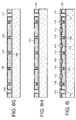
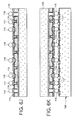
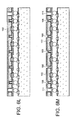
- Figures 6A-6N illustrate the production of a hybridized photodetector matrix on a read circuit according to the second mode of embodiment of the invention.
- Figures 6A to 6I illustrate the achievement of the matrix of photodetectors only.
- Figures 6J to 6N illustrate the hybridization of the matrix of photodetectors to its reading circuit. All of these Figures are cross-sectional views.
- Figure 6A shows a SOI 100 substrate consisting of a supporting silicon support 103 successively a layer of silicon oxide 102 and a thin layer of silicon 101.
- the thin layer of silicon 101 undergoes a oxidation step to get a layer of passivation of surface and protection 104 (see Figure 6B).
- the layer 104 has a thickness of the order of 0.5 ⁇ m.
- Trenches are then made in the thin layer 101.
- a layer of resin is first deposited on the oxide layer 104, then is photolithographed to make an engraving of the oxide layer 104 at the locations provided for trenches.
- the resin is removed.
- the trenches are then engraved in the thin layer of silicon 101.
- the 105 inner trenches are wider in width restricted than the outer trenches. As a result, trenches 105 do not reach the buried oxide layer 102 while the trenches 106 reach layer 102, the engraving being more fast in big patterns than in small ones. This is what is shown in Figure 6C.
- Anisotropic etching is then carried out oxide to remove the oxide layer present in the trench bottom 105 and expose the material semiconductor 101 at the bottom of these trenches. Through against, the initial oxide layer 104 on the layer thin silicon 101 and the buried oxide layer 102 still have sufficient thickness. That's what shows Figure 6E.
- Dopants are then implanted in the exposed parts of the thin layer of material semiconductor 101, at the bottom of the trenches 105. On then proceeds to disseminate the dopants through a annealed to get the doped areas 108 as the shows Figure 6F.
- a layer of resin is then deposited on the oxide layer 104.
- the oxide layer 104 is etched to expose locally the thin layer of semiconductor material 101. This is shown in Figure 6H.
- Dopants complementary to the dopants of zones 108 are implanted in the exposed parts of the thin layer 101 to obtain doped zones 112 (see Figure 6I).
- the remaining resin is removed.
- a metal layer is then uniformly deposited.
- a layer of resin is deposited on this layer metallic.
- photolithography we proceed to etching of the metal layer and the resin is withdrawn.
- a common electrode 114 electrically connected to the conductive walls 110 and contact pads 115 connected to the conductive bushings 111.
- Figure 6J shows the structure obtained after the formation of the conductive balls 116 on the connection pads 113, conductive balls 117 on the common electrode 114 and conductive balls 118 on the contact pads 115. Another way to do is to form the fusible beads on the circuit of reading.
- Figure 6K shows the result of hybridization by "flip chip" of the matrix of photodetectors on a reading circuit 120 by means of fusible beads 116, 117 and 118.
- a filling at means of an insulating material can be achieved between the matrix of photodetectors and the read circuit.
- a layer of resin is then deposited on the oxide layer 102.
- photolithography etching the oxide layer 102 to expose the conductive bushings 111 and the zones implanted 108.
- the resin is removed. We get the structure shown in Figure 6M.
- a metal layer is deposited on the etched oxide layer 102.
- a layer of resin is deposited on the metal layer. Through photolithography, we proceed to the etching of the layer metal with control of the slope of the engravings. The resin is removed and one gets the structure represented in FIG. 6N comprising the electrode common 119 on the receiving side of the light at detect.
- steps may follow, for example a step of cutting the flea structures at the end of a collective process. Before this cutting step, other steps can be added to create filters or anti-reflective layers. The order of the steps is not necessarily the one indicated above.
Landscapes
- Solid State Image Pick-Up Elements (AREA)
- Transforming Light Signals Into Electric Signals (AREA)
- Light Receiving Elements (AREA)
- Facsimile Heads (AREA)
Abstract
Description
- la figure 1 est une vue en coupe transversale d'une matrice de photodétecteurs hybridée sur un circuit de lecture, selon un premier mode de réalisation de l'invention,
- la figure 2 est une vue de dessus de la figure 1 selon la coupe II-II,
- la figure 3 est une vue en coupe transversale d'une variante de réalisation d'une matrice de photodétecteurs hybridée sur un circuit de lecture, selon le premier mode de réalisation de l'invention,
- la figure 4 est une vue en coupe transversale d'une matrice de photodétecteurs hybridée sur un circuit de lecture, selon un deuxième mode de réalisation de l'invention,
- la figure 5 est une vue en coupe transversale d'une variante de réalisation d'une matrice de photodétecteurs hybridée sur un circuit de lecture, selon le deuxième mode de réalisation de l'invention,
- les figures 6A à 6N illustrent la réalisation d'une matrice de photodétecteurs hybridée sur un circuit de lecture selon le deuxième mode de réalisation de l'invention.
- oxydation de surface pour obtenir une couche d'isolation 109 sur les zones dopées 108,
- remplissage des tranchées 105 et 106 par un matériau conducteur, par exemple du polysilicium,
- élimination du surplus de remplissage par polissage mécano-chimique pour obtenir des parois électriquement conductrices 110 et des traversées conductrices 111.
- toute la surface de la matrice contribue à la collecte de la lumière,
- les pixels sont isolés électriquement les uns des autres et ne peuvent pas échanger leurs charges,
- les résistances d'interconnexions sont minimales,
- l'hybridation sur un circuit amplificateur est conservée,
- le nombre de connexions avec le circuit amplificateur est minimum,
- la taille des zones dopées est ajustable selon le signal optique à détecter,
- les pertes de lumière sont minimisées par réflexion sur les faces avant et arrière des métallisations conductrices,
- tous les contacts de sortie des signaux vers l'extérieur, peuvent être pris sur la face supérieure de la matrice en bord de zone éclairée,
- l'ajout de composants optiques tel que couche antireflet ou filtre optique ou concentrateur de lumière est toujours possible.
Claims (14)
- Matrice de photodétecteurs (10, 50) destinée à être hybridée sur un circuit de lecture et constituée à partir d'une plaque de matériau semiconducteur (11, 51) présentant une face de réception d'une lumière à détecter et une face opposée dite face d'hybridation, caractérisée en ce que la plaque est divisée en pixels (12, 52), chaque pixel constituant un photodétecteur, les pixels étant séparés les uns des autres par des moyens de séparation formés transversalement dans la plaque et comprenant une photogrille pour les photodétecteurs, chaque photodétecteur présentant, sur la face d'hybridation, un plot de connexion (18, 58) permettant d'hybrider la matrice de photodétecteurs au circuit de lecture.
- Matrice de photodétecteurs selon la revendication 1, caractérisée en ce que les moyens de séparation comprennent des murs comprenant une paroi électriquement conductrice (13) prise en sandwich entre des parois électriquement isolantes (14, 15), constituant ainsi avec le matériau semiconducteur de la plaque (11) adjacent au mur une photogrille de type MOS, chaque photodétecteur comprenant une première zone dopée (16) et une deuxième zone dopée (17), les premières zones dopées (16) assurant les prises de contact électrique avec les plots de connexion (18) des photodétecteurs, les deuxièmes zones dopées (17) assurant les prises de contact électrique avec une première électrode commune (19), dite électrode de base commune des pixels, située sur la face d'hybridation, les parois électriquement conductrices des murs (13) étant reliées à une deuxième électrode commune (21) située sur la face d'hybridation.
- Matrice de photodétecteurs selon la revendication 2, caractérisée en ce que la première électrode commune (19) et la deuxième électrode commune (21) forment des peignes interdigités.
- Matrice de photodétecteurs selon l'une des revendications 2 ou 3, caractérisée en ce que le matériau semiconducteur est en silicium, la paroi électriquement conductrice (13) des murs est en polysilicium dopé et les parois électriquement isolantes (14, 15) des murs sont en oxyde de silicium.
- Matrice de photodétecteurs selon l'une quelconque des revendications 2 à 4, caractérisée en ce que les premières zones dopées (16) sont des zones suffisamment étendues pour atteindre la photogrille de type MOS.
- Matrice de photodétecteurs selon la revendication 1, caractérisée en ce que les moyens de séparation comprennent des murs comprenant une paroi électriquement conductrice (53) débouchant sur la face d'hybridation de la plaque (51) et se prolongeant à l'intérieur de la plaque en étant recouverte d'une couche de matériau électriquement isolant (54) jusqu'à un sommet n'atteignant pas la face de réception d'une lumière, constituant ainsi avec le matériau semiconducteur de la plaque adjacent au mur photogrille de type MOS, chaque photodétecteur (52) comprenant une première zone dopée (56) et une deuxième zone dopée (57), les premières zones dopées (56) assurant les prises de contact électrique avec les plots de connexion (71) des photodétecteurs, les deuxièmes zones dopées (57) étant situées entre la face de réception d'une lumière et le sommet des murs et assurant des prises de contact électrique avec une première électrode commune (59) située sur la face de réception d'une lumière, la face d'hybridation supportant une deuxième électrode commune (61) reliant électriquement les parois électriquement conductrices des murs qui y débouchent.
- Matrice de photodétecteurs selon la revendication 6, caractérisée en ce qu'elle comprend des moyens de liaison électrique (79) traversant la plaque de matériau semiconducteur pour relier la première électrode commune (59) à une plage conductrice (69) située sur la face d'hybridation.
- Matrice de photodétecteurs selon l'une des revendications 6 ou 7, caractérisée en ce que la première électrode commune (59) comprend des conducteurs électriques possédant une forme permettant de réfléchir la lumière à détecter vers les parties de la face de réception dépourvues de conducteurs électriques.
- Matrice de photodétecteurs selon la revendication 8, caractérisée en ce que ladite forme des conducteurs électriques est une pointe dirigée vers la lumière à détecter.
- Matrice de photodétecteurs selon l'une quelconque des revendications 6 à 9, caractérisée en ce que la deuxième électrode commune (61) présente des parties situées en vis-à-vis de la plaque de matériau semiconducteur (51) de surface adaptée pour permettre de réfléchir sur le matériau semiconducteur une fraction de lumière à détecter qui traverse la plaque de matériau semiconducteur.
- Matrice de photodétecteurs selon l'une quelconque des revendications 6 à 10, caractérisée en ce que le matériau semiconducteur est en silicium, la paroi électriquement conductrice (53) est en polysilicium dopé et la couche de matériau électriquement isolant (54) est en oxyde de silicium.
- Matrice de photodétecteurs selon l'une quelconque des revendications 6 à 11, caractérisée en ce que les premières zones dopées (56) sont des zones suffisamment étendues pour atteindre la photogrille de type MOS.
- Matrice de photodétecteurs selon l'une quelconque des revendications 1 à 12, caractérisée en ce que les zones dopées sont des zones à dopage multiple, de profondeur différente et de type identique ou complémentaire.
- Matrice de photodétecteurs selon l'une quelconque des revendications 2 à 13, caractérisée en ce que les murs comprenant une paroi électriquement conductrice sont alignés dans une première direction, des murs isolants étant alignés dans une deuxième direction qui est transversale à la première direction, les parois électriquement conductrices constituant des lignes de pilotage de photogrille indépendantes.
Applications Claiming Priority (2)
| Application Number | Priority Date | Filing Date | Title |
|---|---|---|---|
| FR0204614A FR2838565B1 (fr) | 2002-04-12 | 2002-04-12 | Matrice de photodetecteurs, a pixels isoles et grille de stockage, hybridee sur un circuit de lecture |
| FR0204614 | 2002-04-12 |
Publications (2)
| Publication Number | Publication Date |
|---|---|
| EP1353381A1 true EP1353381A1 (fr) | 2003-10-15 |
| EP1353381B1 EP1353381B1 (fr) | 2007-10-31 |
Family
ID=28052279
Family Applications (1)
| Application Number | Title | Priority Date | Filing Date |
|---|---|---|---|
| EP03100971A Expired - Lifetime EP1353381B1 (fr) | 2002-04-12 | 2003-04-10 | Matrice de photodetecteurs, à pixels isolés et grillé de stockage, hybridee sur un circuit de lecture |
Country Status (6)
| Country | Link |
|---|---|
| US (1) | US7271375B2 (fr) |
| EP (1) | EP1353381B1 (fr) |
| JP (1) | JP4545387B2 (fr) |
| AT (1) | ATE377260T1 (fr) |
| DE (1) | DE60317133T2 (fr) |
| FR (1) | FR2838565B1 (fr) |
Families Citing this family (12)
| Publication number | Priority date | Publication date | Assignee | Title |
|---|---|---|---|---|
| JP4166471B2 (ja) * | 2001-12-28 | 2008-10-15 | 三菱電機株式会社 | 光モジュール |
| US7425460B2 (en) * | 2004-09-17 | 2008-09-16 | California Institute Of Technology | Method for implementation of back-illuminated CMOS or CCD imagers |
| DE102004060365B4 (de) * | 2004-12-15 | 2009-03-19 | Austriamicrosystems Ag | Bauelement mit Halbleiterübergang und Verfahren zur Herstellung |
| KR100610481B1 (ko) * | 2004-12-30 | 2006-08-08 | 매그나칩 반도체 유한회사 | 수광영역을 넓힌 이미지센서 및 그 제조 방법 |
| KR100718878B1 (ko) | 2005-06-28 | 2007-05-17 | (주)실리콘화일 | 3차원 구조를 갖는 이미지 센서의 분리형 단위화소 및 그제조방법 |
| WO2007059283A2 (fr) | 2005-11-15 | 2007-05-24 | California Institute Of Technology | Dispositif d'imagerie retro-eclaire et procede de fabrication de connexions electriques et optiques sur ce dernier |
| JP2008131169A (ja) * | 2006-11-17 | 2008-06-05 | Shimadzu Corp | 撮像素子およびそれを用いた撮像装置 |
| KR100954927B1 (ko) * | 2007-12-14 | 2010-04-27 | 주식회사 동부하이텍 | 이미지 센서 및 그 제조방법 |
| US7774070B2 (en) * | 2008-01-10 | 2010-08-10 | Hill Laboratories Company | Medical electrode assembly for electrotherapy and phototherapy treatment |
| FR2947952B1 (fr) | 2009-07-07 | 2011-11-25 | Commissariat Energie Atomique | Dispositif photo-detecteur et procede de realisation de dispositif photo-detecteur |
| US9324747B2 (en) | 2014-03-13 | 2016-04-26 | Semiconductor Energy Laboratory Co., Ltd. | Imaging device |
| CN116413729B (zh) * | 2021-12-31 | 2026-03-13 | 华为技术有限公司 | 一种平衡光电探测器、测距装置和测速装置 |
Citations (2)
| Publication number | Priority date | Publication date | Assignee | Title |
|---|---|---|---|---|
| US4684812A (en) * | 1983-08-31 | 1987-08-04 | Texas Instruments Incorporated | Switching circuit for a detector array |
| EP0820104A2 (fr) * | 1996-07-15 | 1998-01-21 | HE HOLDINGS, INC. dba HUGHES ELECTRONICS | Capteur d'image pour lumière de bas niveau ayant une réponse en longueur d'onde étendue utilisant des matériaux semi-conducteurs joints de façon atomique |
Family Cites Families (12)
| Publication number | Priority date | Publication date | Assignee | Title |
|---|---|---|---|---|
| JPS6413766A (en) * | 1987-07-07 | 1989-01-18 | Nec Corp | Infrared image sensing element |
| US4783594A (en) * | 1987-11-20 | 1988-11-08 | Santa Barbara Research Center | Reticular detector array |
| JPH01205465A (ja) * | 1988-02-10 | 1989-08-17 | Sony Corp | 固体撮像装置及びその製造方法 |
| JPH0714996A (ja) * | 1993-06-18 | 1995-01-17 | Mitsubishi Electric Corp | 赤外線検出器とその製造方法 |
| FR2712693B1 (fr) * | 1993-11-17 | 1995-12-15 | Commissariat Energie Atomique | Dispositif de détection de rayonnement, à éléments de détection aboutés, et procédé de fabrication de ce dispositif. |
| US5563405A (en) * | 1995-04-28 | 1996-10-08 | Santa Barbara Research Center | Staring IR-FPA with on-FPA adaptive dynamic range control electronics |
| JP3577368B2 (ja) * | 1995-08-25 | 2004-10-13 | 株式会社東芝 | ハイブリッド型赤外線検出器 |
| JP4571267B2 (ja) * | 2000-04-04 | 2010-10-27 | 浜松ホトニクス株式会社 | 放射線検出器 |
| JP3713418B2 (ja) | 2000-05-30 | 2005-11-09 | 光正 小柳 | 3次元画像処理装置の製造方法 |
| JP4653336B2 (ja) * | 2001-04-18 | 2011-03-16 | 浜松ホトニクス株式会社 | エネルギー線検出器及び装置 |
| JP2003086827A (ja) * | 2001-09-12 | 2003-03-20 | Hamamatsu Photonics Kk | ホトダイオードアレイ、固体撮像装置、及び、放射線検出器 |
| FR2838561B1 (fr) * | 2002-04-12 | 2004-09-17 | Commissariat Energie Atomique | Matrice de photodectecteurs, a pixels isoles par des murs, hybridee sur un circuit de lecture |
-
2002
- 2002-04-12 FR FR0204614A patent/FR2838565B1/fr not_active Expired - Fee Related
-
2003
- 2003-04-08 US US10/408,557 patent/US7271375B2/en not_active Expired - Fee Related
- 2003-04-10 DE DE60317133T patent/DE60317133T2/de not_active Expired - Lifetime
- 2003-04-10 EP EP03100971A patent/EP1353381B1/fr not_active Expired - Lifetime
- 2003-04-10 JP JP2003106944A patent/JP4545387B2/ja not_active Expired - Fee Related
- 2003-04-10 AT AT03100971T patent/ATE377260T1/de not_active IP Right Cessation
Patent Citations (2)
| Publication number | Priority date | Publication date | Assignee | Title |
|---|---|---|---|---|
| US4684812A (en) * | 1983-08-31 | 1987-08-04 | Texas Instruments Incorporated | Switching circuit for a detector array |
| EP0820104A2 (fr) * | 1996-07-15 | 1998-01-21 | HE HOLDINGS, INC. dba HUGHES ELECTRONICS | Capteur d'image pour lumière de bas niveau ayant une réponse en longueur d'onde étendue utilisant des matériaux semi-conducteurs joints de façon atomique |
Also Published As
| Publication number | Publication date |
|---|---|
| FR2838565B1 (fr) | 2004-06-25 |
| DE60317133T2 (de) | 2008-10-02 |
| ATE377260T1 (de) | 2007-11-15 |
| DE60317133D1 (de) | 2007-12-13 |
| JP2003347536A (ja) | 2003-12-05 |
| EP1353381B1 (fr) | 2007-10-31 |
| JP4545387B2 (ja) | 2010-09-15 |
| US7271375B2 (en) | 2007-09-18 |
| US20030222204A1 (en) | 2003-12-04 |
| FR2838565A1 (fr) | 2003-10-17 |
Similar Documents
| Publication | Publication Date | Title |
|---|---|---|
| EP1495494B1 (fr) | Matrice de photodetecteurs, a pixels isoles par des murs, hybridee sur un circuit de lecture | |
| US6034407A (en) | Multi-spectral planar photodiode infrared radiation detector pixels | |
| EP0977269B1 (fr) | Capteur d'image à réseau de photodiodes | |
| EP1421623B1 (fr) | Capteur d'image couleur a colorimetrie amelioree et procede de fabrication | |
| FR2930676A1 (fr) | Capteur d'image de tres faibles dimensions | |
| EP1353381B1 (fr) | Matrice de photodetecteurs, à pixels isolés et grillé de stockage, hybridee sur un circuit de lecture | |
| EP2315251A1 (fr) | Capteur d'image à grille de transfert verticale et son procédé de fabrication | |
| EP2339640A1 (fr) | Photodétecteur à structure plasmon | |
| EP3016141A1 (fr) | Capteur d'image à électrodes verticales | |
| EP1599906B1 (fr) | Matrice de pixels detecteurs integree sur circuit de lecture de charges | |
| WO2011069880A1 (fr) | Capteur d'image multilineaire a integration de charges | |
| EP2452361B1 (fr) | Dispositif photo-détecteur et procédé de réalisation de dispositif photo-détecteur | |
| EP2432033B1 (fr) | Détecteur bispectral multicouche à photodiodes | |
| EP1573821A1 (fr) | Matrice de detecteurs multispectraux | |
| WO2023110412A1 (fr) | Capteur d'images visibles et infrarouges et procédé de fabrication d'un tel capteur | |
| FR3083001A1 (fr) | Capteur d'images | |
| FR2966678A1 (fr) | Dispositif d'imagerie en particulier du type cmos a report et integration. | |
| WO2023117703A1 (fr) | Capteur d'images | |
| WO2023006529A1 (fr) | Capteur d'images | |
| FR3155090A1 (fr) | Capteur d’images | |
| FR3154231A1 (fr) | dispositif imageur d’acquisition d’une image visible et d’une image infrarouge | |
| FR3163771A1 (fr) | Dispositif électronique comprenant une photodiode à base de boîtes quantiques | |
| EP4191676A1 (fr) | Dispositif d'imagerie a rayons x | |
| FR3153186A1 (fr) | Réseau imageur à photodiodes convexes | |
| FR2887076A1 (fr) | Capteur d'image a substrat semiconducteur aminci avec metallisation arriere |
Legal Events
| Date | Code | Title | Description |
|---|---|---|---|
| PUAI | Public reference made under article 153(3) epc to a published international application that has entered the european phase |
Free format text: ORIGINAL CODE: 0009012 |
|
| AK | Designated contracting states |
Kind code of ref document: A1 Designated state(s): AT BE BG CH CY CZ DE DK EE ES FI FR GB GR HU IE IT LI LU MC NL PT RO SE SI SK TR |
|
| AX | Request for extension of the european patent |
Extension state: AL LT LV MK |
|
| 17P | Request for examination filed |
Effective date: 20040320 |
|
| AKX | Designation fees paid |
Designated state(s): AT BE BG CH CY CZ DE DK EE ES FI FR GB GR HU IE IT LI LU MC NL PT RO SE SI SK TR |
|
| RAP1 | Party data changed (applicant data changed or rights of an application transferred) |
Owner name: COMMISSARIAT A L'ENERGIE ATOMIQUE |
|
| 17Q | First examination report despatched |
Effective date: 20061017 |
|
| GRAP | Despatch of communication of intention to grant a patent |
Free format text: ORIGINAL CODE: EPIDOSNIGR1 |
|
| GRAS | Grant fee paid |
Free format text: ORIGINAL CODE: EPIDOSNIGR3 |
|
| GRAA | (expected) grant |
Free format text: ORIGINAL CODE: 0009210 |
|
| AK | Designated contracting states |
Kind code of ref document: B1 Designated state(s): AT BE BG CH CY CZ DE DK EE ES FI FR GB GR HU IE IT LI LU MC NL PT RO SE SI SK TR |
|
| REG | Reference to a national code |
Ref country code: GB Ref legal event code: FG4D Free format text: NOT ENGLISH |
|
| REG | Reference to a national code |
Ref country code: IE Ref legal event code: FG4D Free format text: LANGUAGE OF EP DOCUMENT: FRENCH |
|
| REG | Reference to a national code |
Ref country code: CH Ref legal event code: EP |
|
| REF | Corresponds to: |
Ref document number: 60317133 Country of ref document: DE Date of ref document: 20071213 Kind code of ref document: P |
|
| GBT | Gb: translation of ep patent filed (gb section 77(6)(a)/1977) |
Effective date: 20080116 |
|
| NLV1 | Nl: lapsed or annulled due to failure to fulfill the requirements of art. 29p and 29m of the patents act | ||
| PG25 | Lapsed in a contracting state [announced via postgrant information from national office to epo] |
Ref country code: SE Free format text: LAPSE BECAUSE OF FAILURE TO SUBMIT A TRANSLATION OF THE DESCRIPTION OR TO PAY THE FEE WITHIN THE PRESCRIBED TIME-LIMIT Effective date: 20080131 Ref country code: NL Free format text: LAPSE BECAUSE OF FAILURE TO SUBMIT A TRANSLATION OF THE DESCRIPTION OR TO PAY THE FEE WITHIN THE PRESCRIBED TIME-LIMIT Effective date: 20071031 Ref country code: ES Free format text: LAPSE BECAUSE OF FAILURE TO SUBMIT A TRANSLATION OF THE DESCRIPTION OR TO PAY THE FEE WITHIN THE PRESCRIBED TIME-LIMIT Effective date: 20080211 |
|
| PG25 | Lapsed in a contracting state [announced via postgrant information from national office to epo] |
Ref country code: PT Free format text: LAPSE BECAUSE OF FAILURE TO SUBMIT A TRANSLATION OF THE DESCRIPTION OR TO PAY THE FEE WITHIN THE PRESCRIBED TIME-LIMIT Effective date: 20080331 Ref country code: SI Free format text: LAPSE BECAUSE OF FAILURE TO SUBMIT A TRANSLATION OF THE DESCRIPTION OR TO PAY THE FEE WITHIN THE PRESCRIBED TIME-LIMIT Effective date: 20071031 Ref country code: BG Free format text: LAPSE BECAUSE OF FAILURE TO SUBMIT A TRANSLATION OF THE DESCRIPTION OR TO PAY THE FEE WITHIN THE PRESCRIBED TIME-LIMIT Effective date: 20080131 |
|
| REG | Reference to a national code |
Ref country code: IE Ref legal event code: FD4D |
|
| PG25 | Lapsed in a contracting state [announced via postgrant information from national office to epo] |
Ref country code: AT Free format text: LAPSE BECAUSE OF FAILURE TO SUBMIT A TRANSLATION OF THE DESCRIPTION OR TO PAY THE FEE WITHIN THE PRESCRIBED TIME-LIMIT Effective date: 20071031 |
|
| PG25 | Lapsed in a contracting state [announced via postgrant information from national office to epo] |
Ref country code: DK Free format text: LAPSE BECAUSE OF FAILURE TO SUBMIT A TRANSLATION OF THE DESCRIPTION OR TO PAY THE FEE WITHIN THE PRESCRIBED TIME-LIMIT Effective date: 20071031 Ref country code: CZ Free format text: LAPSE BECAUSE OF FAILURE TO SUBMIT A TRANSLATION OF THE DESCRIPTION OR TO PAY THE FEE WITHIN THE PRESCRIBED TIME-LIMIT Effective date: 20071031 |
|
| PG25 | Lapsed in a contracting state [announced via postgrant information from national office to epo] |
Ref country code: SK Free format text: LAPSE BECAUSE OF FAILURE TO SUBMIT A TRANSLATION OF THE DESCRIPTION OR TO PAY THE FEE WITHIN THE PRESCRIBED TIME-LIMIT Effective date: 20071031 Ref country code: RO Free format text: LAPSE BECAUSE OF FAILURE TO SUBMIT A TRANSLATION OF THE DESCRIPTION OR TO PAY THE FEE WITHIN THE PRESCRIBED TIME-LIMIT Effective date: 20071031 |
|
| PLBE | No opposition filed within time limit |
Free format text: ORIGINAL CODE: 0009261 |
|
| STAA | Information on the status of an ep patent application or granted ep patent |
Free format text: STATUS: NO OPPOSITION FILED WITHIN TIME LIMIT |
|
| 26N | No opposition filed |
Effective date: 20080801 |
|
| BERE | Be: lapsed |
Owner name: COMMISSARIAT A L'ENERGIE ATOMIQUE Effective date: 20080430 |
|
| PG25 | Lapsed in a contracting state [announced via postgrant information from national office to epo] |
Ref country code: IE Free format text: LAPSE BECAUSE OF FAILURE TO SUBMIT A TRANSLATION OF THE DESCRIPTION OR TO PAY THE FEE WITHIN THE PRESCRIBED TIME-LIMIT Effective date: 20071031 |
|
| PG25 | Lapsed in a contracting state [announced via postgrant information from national office to epo] |
Ref country code: MC Free format text: LAPSE BECAUSE OF NON-PAYMENT OF DUE FEES Effective date: 20080430 |
|
| REG | Reference to a national code |
Ref country code: CH Ref legal event code: PL |
|
| PG25 | Lapsed in a contracting state [announced via postgrant information from national office to epo] |
Ref country code: LI Free format text: LAPSE BECAUSE OF NON-PAYMENT OF DUE FEES Effective date: 20080430 Ref country code: EE Free format text: LAPSE BECAUSE OF FAILURE TO SUBMIT A TRANSLATION OF THE DESCRIPTION OR TO PAY THE FEE WITHIN THE PRESCRIBED TIME-LIMIT Effective date: 20071031 Ref country code: GR Free format text: LAPSE BECAUSE OF FAILURE TO SUBMIT A TRANSLATION OF THE DESCRIPTION OR TO PAY THE FEE WITHIN THE PRESCRIBED TIME-LIMIT Effective date: 20080201 Ref country code: CH Free format text: LAPSE BECAUSE OF NON-PAYMENT OF DUE FEES Effective date: 20080430 |
|
| PG25 | Lapsed in a contracting state [announced via postgrant information from national office to epo] |
Ref country code: FI Free format text: LAPSE BECAUSE OF FAILURE TO SUBMIT A TRANSLATION OF THE DESCRIPTION OR TO PAY THE FEE WITHIN THE PRESCRIBED TIME-LIMIT Effective date: 20071031 |
|
| PG25 | Lapsed in a contracting state [announced via postgrant information from national office to epo] |
Ref country code: BE Free format text: LAPSE BECAUSE OF NON-PAYMENT OF DUE FEES Effective date: 20080430 |
|
| PG25 | Lapsed in a contracting state [announced via postgrant information from national office to epo] |
Ref country code: CY Free format text: LAPSE BECAUSE OF FAILURE TO SUBMIT A TRANSLATION OF THE DESCRIPTION OR TO PAY THE FEE WITHIN THE PRESCRIBED TIME-LIMIT Effective date: 20071031 |
|
| PG25 | Lapsed in a contracting state [announced via postgrant information from national office to epo] |
Ref country code: LU Free format text: LAPSE BECAUSE OF NON-PAYMENT OF DUE FEES Effective date: 20080410 Ref country code: HU Free format text: LAPSE BECAUSE OF FAILURE TO SUBMIT A TRANSLATION OF THE DESCRIPTION OR TO PAY THE FEE WITHIN THE PRESCRIBED TIME-LIMIT Effective date: 20080501 |
|
| PG25 | Lapsed in a contracting state [announced via postgrant information from national office to epo] |
Ref country code: TR Free format text: LAPSE BECAUSE OF FAILURE TO SUBMIT A TRANSLATION OF THE DESCRIPTION OR TO PAY THE FEE WITHIN THE PRESCRIBED TIME-LIMIT Effective date: 20071031 |
|
| REG | Reference to a national code |
Ref country code: FR Ref legal event code: PLFP Year of fee payment: 14 |
|
| REG | Reference to a national code |
Ref country code: FR Ref legal event code: PLFP Year of fee payment: 15 |
|
| REG | Reference to a national code |
Ref country code: FR Ref legal event code: PLFP Year of fee payment: 16 |
|
| PGFP | Annual fee paid to national office [announced via postgrant information from national office to epo] |
Ref country code: DE Payment date: 20180409 Year of fee payment: 16 |
|
| PGFP | Annual fee paid to national office [announced via postgrant information from national office to epo] |
Ref country code: IT Payment date: 20180417 Year of fee payment: 16 Ref country code: FR Payment date: 20180426 Year of fee payment: 16 |
|
| PGFP | Annual fee paid to national office [announced via postgrant information from national office to epo] |
Ref country code: GB Payment date: 20180417 Year of fee payment: 16 |
|
| REG | Reference to a national code |
Ref country code: DE Ref legal event code: R119 Ref document number: 60317133 Country of ref document: DE |
|
| GBPC | Gb: european patent ceased through non-payment of renewal fee |
Effective date: 20190410 |
|
| PG25 | Lapsed in a contracting state [announced via postgrant information from national office to epo] |
Ref country code: DE Free format text: LAPSE BECAUSE OF NON-PAYMENT OF DUE FEES Effective date: 20191101 Ref country code: GB Free format text: LAPSE BECAUSE OF NON-PAYMENT OF DUE FEES Effective date: 20190410 |
|
| PG25 | Lapsed in a contracting state [announced via postgrant information from national office to epo] |
Ref country code: IT Free format text: LAPSE BECAUSE OF NON-PAYMENT OF DUE FEES Effective date: 20190410 |
|
| PG25 | Lapsed in a contracting state [announced via postgrant information from national office to epo] |
Ref country code: FR Free format text: LAPSE BECAUSE OF NON-PAYMENT OF DUE FEES Effective date: 20190430 |