EP1351061B1 - Power switch with current sense circuit - Google Patents
Power switch with current sense circuit Download PDFInfo
- Publication number
- EP1351061B1 EP1351061B1 EP02392004A EP02392004A EP1351061B1 EP 1351061 B1 EP1351061 B1 EP 1351061B1 EP 02392004 A EP02392004 A EP 02392004A EP 02392004 A EP02392004 A EP 02392004A EP 1351061 B1 EP1351061 B1 EP 1351061B1
- Authority
- EP
- European Patent Office
- Prior art keywords
- transistor
- output
- current
- drain
- coupled
- Prior art date
- Legal status (The legal status is an assumption and is not a legal conclusion. Google has not performed a legal analysis and makes no representation as to the accuracy of the status listed.)
- Expired - Lifetime
Links
- 239000003990 capacitor Substances 0.000 claims description 18
- 230000010355 oscillation Effects 0.000 claims 1
- 230000008878 coupling Effects 0.000 description 2
- 238000010168 coupling process Methods 0.000 description 2
- 238000005859 coupling reaction Methods 0.000 description 2
- 238000000034 method Methods 0.000 description 2
- 239000004065 semiconductor Substances 0.000 description 2
- 208000017604 Hodgkin disease Diseases 0.000 description 1
- 239000000446 fuel Substances 0.000 description 1
- 230000036039 immunity Effects 0.000 description 1
- 230000001939 inductive effect Effects 0.000 description 1
- 239000000463 material Substances 0.000 description 1
- 238000005259 measurement Methods 0.000 description 1
- 238000009966 trimming Methods 0.000 description 1
Images

Classifications
-
- G—PHYSICS
- G01—MEASURING; TESTING
- G01R—MEASURING ELECTRIC VARIABLES; MEASURING MAGNETIC VARIABLES
- G01R19/00—Arrangements for measuring currents or voltages or for indicating presence or sign thereof
-
- G—PHYSICS
- G01—MEASURING; TESTING
- G01R—MEASURING ELECTRIC VARIABLES; MEASURING MAGNETIC VARIABLES
- G01R19/00—Arrangements for measuring currents or voltages or for indicating presence or sign thereof
- G01R19/0092—Arrangements for measuring currents or voltages or for indicating presence or sign thereof measuring current only
-
- G—PHYSICS
- G01—MEASURING; TESTING
- G01R—MEASURING ELECTRIC VARIABLES; MEASURING MAGNETIC VARIABLES
- G01R19/00—Arrangements for measuring currents or voltages or for indicating presence or sign thereof
- G01R19/25—Arrangements for measuring currents or voltages or for indicating presence or sign thereof using digital measurement techniques
- G01R19/252—Arrangements for measuring currents or voltages or for indicating presence or sign thereof using digital measurement techniques using analogue/digital converters of the type with conversion of voltage or current into frequency and measuring of this frequency
Definitions
- Another further object of the present invention is to provide a digital frequency signal in proportion to the power switch output current using a current controlled oscillator.
- the output is a high side driver circuit where the CONTROL signal 44 must be substantially higher than the output voltage VOUT and may require a charge pump.
- Other biasing arrangements could be used. This is not a necessary feature of the present invention.
- Z LOAD 32 may comprise a resistive load or an inductive load, such as a coil.
- this circuit may comprise a part of a DC-to-DC converter.
- a means of equalizing 56, or drain coupling 56, the sense transistor NSENSE 28 drain-to-source voltage and the output transistor NOUT 24 drain-to-source voltage is used such that the sense transistor NSENSE drain current I SENSE equals the output current I OUT divided by the sensing factor R.
- a preferred implementation of the drain coupling 56 is shown in Fig. 2 and discussed below.
- a current controlled oscillator (CCO) 40 is included.
- the current controlled oscillator 40 has input 38 and output DATAOUT 48.
- the input to the CCO 40 comprises the sense transistor drain current I SENSE .
- the output DATAOUT 48 comprises a cyclical signal having a frequency proportionial to the output current.
- a preferred implementation of the CCO 40 is shown in Fig. 2 and discussed below.
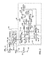
- Fig. 2 a more detailed version of the preferred embodiment of the present invention is shown. Several important features of the present invention are illustrated. Where like features between Figs. 1 and 2 are illustrated, the elements have been numbered the same.
- the means of equalizing 56 the drain voltages of NOUT 24 and NSENSE 28 is shown in detail.
- the means of equalizing 56 the drain voltages of NOUT 24 and NSENSE 28 preferably comprises, first, a first transistor P1 60 having gate, drain, and source.
- the source of P1 60 is coupled to the drain of NSENSE 28.
- the drain of P1 60 is coupled to the drain of NOUT 28.
- a second transistor P2 64 has gate, drain, and source.
- the source of P2 64 is coupled to the sense transistor NSENSE drain.
- the drain of P2 64 is coupled to the current controlled oscillator (CCO) 40 input.
- Both P1 60 and P2 64 preferably comprise PMOS devices.
- An amplifier A1 68 having two inputs and an output completes the means of equalization 56. One input is coupled to the drain of NSENSE 28. The other input is coupled to the drain of NOUT 24. The output of A1 68 is coupled to the P1 60 and P2 64 gates. In this novel configuration, the circuit 56 forces the drain voltages of NOUT 24 and NSENSE 28 to nearly the same voltage while causing the sensing current I SENSE to flow into the CCO circuit 40.
- the circuit 40 preferably comprises, first, a S-R flip-flop 80.
- the S-R flip-flop 80 has set and reset inputs and an output.
- the S-R flip flop 80 output comprises the current controlled oscillator output DATAOUT 48.
- a set comparator QSET 92 has two inputs and an output.
- the negative input of QSET 92 is coupled to a voltage reference VREF 102.
- the output of QSET 92 is coupled to the S-R flip-flop 80 SET input.
- a reset comparator QRST 96 has two inputs and an output.
- the negative input of QRST 96 is coupled to the voltage reference.
- the output of QRST 96 is coupled to the S-R flip-flop 80 RESET input.
- a set current-to-voltage converter 121 comprises the first switch SW SET 122, the capacitor C SET 126, and the second switch NSET 130.
- the set current-to-voltage converter 121 has an input 38 and an output VSET 100.
- the input to the set current-to-voltage converter 121 is the sense current I SENSE , I SENSE is switchably coupled to the SET current-to voltage converter 121 by the first switch SW SET 122.
- I SENSE charges C SET 126 and the current is thereby converted to the voltage VSET 100.
- VSFT 100 is coupled to the positive input of set comparator QSET 92.
- a reset current-to-voltage converter 111 comprises the first switch SW RST 110, the capacitor C RST 114, and the second switch NRST 118.
- the reset current-to-voltage converter 111 has an input 38 and an output VRST 104.
- the input to the set current-to-voltage converter 111 is also the sense current I SENSE .
- I SENSE is switchably coupled to the RESET current-to-voltage converter 111 by the first switch SW RST 110.
- I SENSE charges C RST 114, and the current is thereby converted to the voltage VRST 104.
- VRST 104 is coupled to the positive input of reset comparator QRST 96.
- the CCO circuit 40 operates in either the set or reset mode.
- the S-R flip-flop 80 is set and the DATAOUT signal 48 is high.
- the set second switch NSET 130 is ON and the set first switch SW SET 122 is OFF. Therefore, the VSET 100 node is pulled to ground 36 through NSET 130.
- the reset second switch NRST 118 is OFF and the reset first switch SW RST 110 is ON.
- the sense current I SENSE charges C RST 114, and the current is thereby converted to the voltage VRST 104.
- the reset current-to-voltage converter 111 is in the OFF state where NRST 118 is turned ON and SW RST 110 is turned OFF.
- SW SET 122 is turned ON and NSET 130 is turned OFF. Therefore, the sense current I SENSE charges the set capacitor C SET 126, and VSET 100 increases in voltage.
- VSET 100 exceeds the value VREF 102, the set comparator QSET 92 is toggled.
- the SET signal 84 is asserted. Since the RESET 88 is driven low by NRST 118, the S-R flip-flop 80 is now forced to the SET state again.
- the S-R flip-flop 80 output DATAOUT 48 will cyclically toggle between high and low at a frequency that is directly proportional to the I SENSE current.
- the greater the value of I SENSE the faster the capacitors are charged and the faster DATAOUT 48 cycles. Smaller values of I SENSE reduce the cycle frequency. If the frequency is monitored, the energy of the power switch NOUT 24 can be monitored.
- the novel design includes only the voltage reference VREF 102 that must be calibrated. By calibrating VREF 102, through trimming a resistor value for instance, a correction can be made for process variation in the capacitor values. Further, by using this simple CCO circuit 40, the linearity of the circuit is extremely high. Only the temperature drift of the capacitors C SET 126 and C RST 114 is important. This drift is only 30 ppm, however. Therefore, the system is very stable over temperature.
- the sensing factor R can be adjusted to thereby adjust the dynamic range of the current. For example, for relatively small output currents l OUT , it may be desirable to reduce the sensing factor R so that the sensing current, I SENSE , remains large enough for good noise immunity and frequency output. Alternatively, it may be desirable to increase the sensing factor R when the output current I OUT is very large.
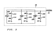
- the sensing transistor 28 is divided into a plurality of sensing transistors, NS1 200, NS2 204, and NS3 208.
- a series of switches SW1 212 through SW6 232 is used to select which of any or which of a combination of the sensing devices are used.
- a circuit of this type could be used to create a range of sensing factors such that, for example, a dynamic range of output current from about 10 microamps to about 3 amps could be converted into proportional frequencies using the same circuit.
- the present invention provides an effective and very manufacturable current sense circuit for a power switch output.
- the current sense circuit generates a sense current using a sense transistor.
- the accuracy of the sense current is improved by equalizing the drain to source voltage for the power transistor and the sense transistor.
- a cyclical output signal is generated having a frequency proportional to the power switch output current using a current controlled oscillator.
- the current sense circuit exhibits a high dynamic range and excellent linearity.
- the sense circuit may have an adjustable sensing factor.
- the novel current sense circuit for a power switch provides an effective and manufacturable alternative to the prior art.
Landscapes
- Physics & Mathematics (AREA)
- General Physics & Mathematics (AREA)
- Dc-Dc Converters (AREA)
- Measurement Of Current Or Voltage (AREA)
- Emergency Protection Circuit Devices (AREA)
- Driving Mechanisms And Operating Circuits Of Arc-Extinguishing High-Tension Switches (AREA)
- Electronic Switches (AREA)
Priority Applications (7)
| Application Number | Priority Date | Filing Date | Title |
|---|---|---|---|
| AT02392004T ATE495454T1 (de) | 2002-04-02 | 2002-04-02 | Leistungsschalter mit stromabfühlschaltung |
| DE60238900T DE60238900D1 (de) | 2002-04-02 | 2002-04-02 | Leistungsschalter mit Stromabfühlschaltung |
| EP02392004A EP1351061B1 (en) | 2002-04-02 | 2002-04-02 | Power switch with current sense circuit |
| US10/126,384 US6552579B1 (en) | 2002-04-02 | 2002-04-19 | Fuel gauge power switch with current sense |
| JP2003098428A JP2003315383A (ja) | 2002-04-02 | 2003-04-01 | 電流感知を伴う燃料計電力スイッチ |
| KR1020030020776A KR100627000B1 (ko) | 2002-04-02 | 2003-04-02 | 전류 감지용 연료 게이지 파워 스위치 |
| JP2009240590A JP5222267B2 (ja) | 2002-04-02 | 2009-10-19 | 電流感知を伴う燃料計電力スイッチ |
Applications Claiming Priority (1)
| Application Number | Priority Date | Filing Date | Title |
|---|---|---|---|
| EP02392004A EP1351061B1 (en) | 2002-04-02 | 2002-04-02 | Power switch with current sense circuit |
Publications (2)
| Publication Number | Publication Date |
|---|---|
| EP1351061A1 EP1351061A1 (en) | 2003-10-08 |
| EP1351061B1 true EP1351061B1 (en) | 2011-01-12 |
Family
ID=27838185
Family Applications (1)
| Application Number | Title | Priority Date | Filing Date |
|---|---|---|---|
| EP02392004A Expired - Lifetime EP1351061B1 (en) | 2002-04-02 | 2002-04-02 | Power switch with current sense circuit |
Country Status (6)
| Country | Link |
|---|---|
| US (1) | US6552579B1 (enExample) |
| EP (1) | EP1351061B1 (enExample) |
| JP (2) | JP2003315383A (enExample) |
| KR (1) | KR100627000B1 (enExample) |
| AT (1) | ATE495454T1 (enExample) |
| DE (1) | DE60238900D1 (enExample) |
Families Citing this family (11)
| Publication number | Priority date | Publication date | Assignee | Title |
|---|---|---|---|---|
| JP3770836B2 (ja) * | 2002-01-23 | 2006-04-26 | 株式会社ルネサステクノロジ | 高速に電源スイッチのオンオフが可能な論理回路及び同論理回路における電流低減方法 |
| JP4138708B2 (ja) * | 2004-07-12 | 2008-08-27 | 浜松ホトニクス株式会社 | 光検出装置 |
| GB2428301B (en) * | 2005-07-13 | 2008-02-13 | A D Developments Ltd | Current measurement apparatus |
| US7327130B1 (en) * | 2006-06-21 | 2008-02-05 | Zilker Labs, Inc. | Current sense method |
| US7863908B2 (en) * | 2007-11-16 | 2011-01-04 | Infineon Technologies Ag | Current measurement based on a charge in a capacitor |
| KR101925629B1 (ko) * | 2012-05-08 | 2018-12-05 | 현대모비스 주식회사 | 홀 센서를 이용한 지능형 배터리 센서 장치 |
| KR102349418B1 (ko) | 2015-08-31 | 2022-01-10 | 삼성전자 주식회사 | 기준전류 발생회로 및 기준전류 발생회로를 포함하는 전자 장치 |
| US9621166B1 (en) * | 2015-09-23 | 2017-04-11 | Qualcomm Incorporated | Wide frequency/voltage-ratio buffer with adaptive power consumption |
| CN106405214B (zh) * | 2016-08-18 | 2019-04-05 | 中国航空工业集团公司上海航空测控技术研究所 | 一种压电传感器检测设备 |
| US11047946B2 (en) | 2018-05-08 | 2021-06-29 | Qualcomm Incorporated | Differential current sensing with robust path, voltage offset removal and process, voltage, temperature (PVT) tolerance |
| JP2021047057A (ja) * | 2019-09-17 | 2021-03-25 | ルネサスエレクトロニクス株式会社 | 半導体装置、および、パワーデバイス |
Citations (1)
| Publication number | Priority date | Publication date | Assignee | Title |
|---|---|---|---|---|
| US5614871A (en) * | 1995-01-25 | 1997-03-25 | Nippon Precision Circuits Inc. | Voltage-controlled oscillator circuit |
Family Cites Families (8)
| Publication number | Priority date | Publication date | Assignee | Title |
|---|---|---|---|---|
| US4147996A (en) * | 1978-04-07 | 1979-04-03 | Sprague Electric Company | Current-controlled oscillator |
| US4553084A (en) * | 1984-04-02 | 1985-11-12 | Motorola, Inc. | Current sensing circuit |
| US6201417B1 (en) | 1994-09-02 | 2001-03-13 | Semiconductor Components Industries, Llc. | Shaping a current sense signal by using a controlled slew rate |
| DE19520735C2 (de) * | 1995-06-07 | 1999-07-01 | Siemens Ag | Schaltungsanordnung zum Erfassen des Laststroms eines Leistungs-Halbleiterbauelementes mit sourceseitiger Last |
| US5680034A (en) | 1995-09-22 | 1997-10-21 | Toko, Inc. | PWM controller for resonant converters |
| US5821740A (en) | 1996-02-15 | 1998-10-13 | Harris Corporation | DC-to-DC converter having fast over-current detection and associated methods |
| WO1998007038A1 (de) * | 1996-08-14 | 1998-02-19 | Siemens Aktiengesellschaft | Schaltungsanordnung zum erfassen des laststroms eines leistungs-halbleiterbauelements mit sourceseitiger last |
| US6348806B1 (en) * | 1999-03-18 | 2002-02-19 | Motorola, Inc. | Method and apparatus for measuring gate leakage current in an integrated circuit |
-
2002
- 2002-04-02 EP EP02392004A patent/EP1351061B1/en not_active Expired - Lifetime
- 2002-04-02 AT AT02392004T patent/ATE495454T1/de not_active IP Right Cessation
- 2002-04-02 DE DE60238900T patent/DE60238900D1/de not_active Expired - Lifetime
- 2002-04-19 US US10/126,384 patent/US6552579B1/en not_active Expired - Lifetime
-
2003
- 2003-04-01 JP JP2003098428A patent/JP2003315383A/ja active Pending
- 2003-04-02 KR KR1020030020776A patent/KR100627000B1/ko not_active Expired - Fee Related
-
2009
- 2009-10-19 JP JP2009240590A patent/JP5222267B2/ja not_active Expired - Fee Related
Patent Citations (1)
| Publication number | Priority date | Publication date | Assignee | Title |
|---|---|---|---|---|
| US5614871A (en) * | 1995-01-25 | 1997-03-25 | Nippon Precision Circuits Inc. | Voltage-controlled oscillator circuit |
Also Published As
| Publication number | Publication date |
|---|---|
| ATE495454T1 (de) | 2011-01-15 |
| KR100627000B1 (ko) | 2006-09-22 |
| DE60238900D1 (de) | 2011-02-24 |
| JP2010025946A (ja) | 2010-02-04 |
| EP1351061A1 (en) | 2003-10-08 |
| JP5222267B2 (ja) | 2013-06-26 |
| US6552579B1 (en) | 2003-04-22 |
| KR20030079761A (ko) | 2003-10-10 |
| JP2003315383A (ja) | 2003-11-06 |
Similar Documents
| Publication | Publication Date | Title |
|---|---|---|
| JP5222267B2 (ja) | 電流感知を伴う燃料計電力スイッチ | |
| KR101017656B1 (ko) | 동기 정류형 스위칭 레귤레이터 | |
| US7859324B2 (en) | Power supply unit | |
| US9431845B2 (en) | Switching charger, the control circuit and the control method thereof | |
| KR101037306B1 (ko) | 스위칭 레귤레이터 및 그 펄스폭 조정 방법 | |
| US9391516B2 (en) | Switching charger, the control circuit and the control method thereof | |
| KR101225408B1 (ko) | 콤퍼레이터 방식 dc-dc 컨버터 | |
| US7777467B2 (en) | Voltage rising/falling type switching regulator and operation control method thereof | |
| US6163190A (en) | Hysteresis comparator circuit consuming a small current | |
| US20220247320A1 (en) | Resonant dc-dc converter with average half cycle control | |
| EP1886153B1 (en) | Bi-directional mos current sense circuit | |
| EP3468022A1 (en) | Switch-mode power converter | |
| US7859242B2 (en) | DC-DC Converter | |
| US7663409B2 (en) | Voltage/current converter circuit and method for providing a ramp current | |
| KR101774601B1 (ko) | 스위칭 레귤레이터 제어 회로 및 스위칭 레귤레이터 | |
| CN101079617B (zh) | 精确的定时信号发生器及其方法 | |
| TWI381511B (zh) | 單一接腳多功能信號偵測方法以及用於其之結構 | |
| US20140218075A1 (en) | Adaptive slope generator | |
| CN110247551B (zh) | 电流控制电路及功率变换器 | |
| JP2005110366A (ja) | ドライブ回路 | |
| US20060087296A1 (en) | DC/DC converter | |
| US9952616B2 (en) | Differential circuit including a current mirror | |
| JP2023109886A (ja) | 電圧変化率検出回路、半導体装置及び電力変換器 | |
| US12368366B2 (en) | Methods and systems of current sensing in switching power converters | |
| US10289136B1 (en) | Converting apparatus and method thereof |
Legal Events
| Date | Code | Title | Description |
|---|---|---|---|
| PUAI | Public reference made under article 153(3) epc to a published international application that has entered the european phase |
Free format text: ORIGINAL CODE: 0009012 |
|
| AK | Designated contracting states |
Kind code of ref document: A1 Designated state(s): AT BE CH CY DE DK ES FI FR GB GR IE IT LI LU MC NL PT SE TR |
|
| AX | Request for extension of the european patent |
Extension state: AL LT LV MK RO SI |
|
| 17P | Request for examination filed |
Effective date: 20040407 |
|
| AKX | Designation fees paid |
Designated state(s): AT BE CH CY DE DK ES FI FR GB GR IE IT LI LU MC NL PT SE TR |
|
| 17Q | First examination report despatched |
Effective date: 20060907 |
|
| GRAP | Despatch of communication of intention to grant a patent |
Free format text: ORIGINAL CODE: EPIDOSNIGR1 |
|
| RTI1 | Title (correction) |
Free format text: POWER SWITCH WITH CURRENT SENSE CIRCUIT |
|
| GRAS | Grant fee paid |
Free format text: ORIGINAL CODE: EPIDOSNIGR3 |
|
| GRAA | (expected) grant |
Free format text: ORIGINAL CODE: 0009210 |
|
| AK | Designated contracting states |
Kind code of ref document: B1 Designated state(s): AT BE CH CY DE DK ES FI FR GB GR IE IT LI LU MC NL PT SE TR |
|
| REG | Reference to a national code |
Ref country code: GB Ref legal event code: FG4D |
|
| REG | Reference to a national code |
Ref country code: CH Ref legal event code: EP |
|
| REG | Reference to a national code |
Ref country code: IE Ref legal event code: FG4D |
|
| REF | Corresponds to: |
Ref document number: 60238900 Country of ref document: DE Date of ref document: 20110224 Kind code of ref document: P |
|
| REG | Reference to a national code |
Ref country code: DE Ref legal event code: R096 Ref document number: 60238900 Country of ref document: DE Effective date: 20110224 |
|
| REG | Reference to a national code |
Ref country code: NL Ref legal event code: VDEP Effective date: 20110112 |
|
| PG25 | Lapsed in a contracting state [announced via postgrant information from national office to epo] |
Ref country code: PT Free format text: LAPSE BECAUSE OF FAILURE TO SUBMIT A TRANSLATION OF THE DESCRIPTION OR TO PAY THE FEE WITHIN THE PRESCRIBED TIME-LIMIT Effective date: 20110512 Ref country code: GR Free format text: LAPSE BECAUSE OF FAILURE TO SUBMIT A TRANSLATION OF THE DESCRIPTION OR TO PAY THE FEE WITHIN THE PRESCRIBED TIME-LIMIT Effective date: 20110413 Ref country code: ES Free format text: LAPSE BECAUSE OF FAILURE TO SUBMIT A TRANSLATION OF THE DESCRIPTION OR TO PAY THE FEE WITHIN THE PRESCRIBED TIME-LIMIT Effective date: 20110423 Ref country code: SE Free format text: LAPSE BECAUSE OF FAILURE TO SUBMIT A TRANSLATION OF THE DESCRIPTION OR TO PAY THE FEE WITHIN THE PRESCRIBED TIME-LIMIT Effective date: 20110112 |
|
| PG25 | Lapsed in a contracting state [announced via postgrant information from national office to epo] |
Ref country code: NL Free format text: LAPSE BECAUSE OF FAILURE TO SUBMIT A TRANSLATION OF THE DESCRIPTION OR TO PAY THE FEE WITHIN THE PRESCRIBED TIME-LIMIT Effective date: 20110112 Ref country code: BE Free format text: LAPSE BECAUSE OF FAILURE TO SUBMIT A TRANSLATION OF THE DESCRIPTION OR TO PAY THE FEE WITHIN THE PRESCRIBED TIME-LIMIT Effective date: 20110112 Ref country code: CY Free format text: LAPSE BECAUSE OF FAILURE TO SUBMIT A TRANSLATION OF THE DESCRIPTION OR TO PAY THE FEE WITHIN THE PRESCRIBED TIME-LIMIT Effective date: 20110112 Ref country code: FI Free format text: LAPSE BECAUSE OF FAILURE TO SUBMIT A TRANSLATION OF THE DESCRIPTION OR TO PAY THE FEE WITHIN THE PRESCRIBED TIME-LIMIT Effective date: 20110112 Ref country code: AT Free format text: LAPSE BECAUSE OF FAILURE TO SUBMIT A TRANSLATION OF THE DESCRIPTION OR TO PAY THE FEE WITHIN THE PRESCRIBED TIME-LIMIT Effective date: 20110112 |
|
| PG25 | Lapsed in a contracting state [announced via postgrant information from national office to epo] |
Ref country code: DK Free format text: LAPSE BECAUSE OF FAILURE TO SUBMIT A TRANSLATION OF THE DESCRIPTION OR TO PAY THE FEE WITHIN THE PRESCRIBED TIME-LIMIT Effective date: 20110112 |
|
| PLBE | No opposition filed within time limit |
Free format text: ORIGINAL CODE: 0009261 |
|
| STAA | Information on the status of an ep patent application or granted ep patent |
Free format text: STATUS: NO OPPOSITION FILED WITHIN TIME LIMIT |
|
| PG25 | Lapsed in a contracting state [announced via postgrant information from national office to epo] |
Ref country code: MC Free format text: LAPSE BECAUSE OF NON-PAYMENT OF DUE FEES Effective date: 20110430 |
|
| REG | Reference to a national code |
Ref country code: CH Ref legal event code: PL |
|
| 26N | No opposition filed |
Effective date: 20111013 |
|
| PG25 | Lapsed in a contracting state [announced via postgrant information from national office to epo] |
Ref country code: IT Free format text: LAPSE BECAUSE OF FAILURE TO SUBMIT A TRANSLATION OF THE DESCRIPTION OR TO PAY THE FEE WITHIN THE PRESCRIBED TIME-LIMIT Effective date: 20110112 |
|
| PG25 | Lapsed in a contracting state [announced via postgrant information from national office to epo] |
Ref country code: LI Free format text: LAPSE BECAUSE OF NON-PAYMENT OF DUE FEES Effective date: 20110430 Ref country code: CH Free format text: LAPSE BECAUSE OF NON-PAYMENT OF DUE FEES Effective date: 20110430 |
|
| REG | Reference to a national code |
Ref country code: IE Ref legal event code: MM4A |
|
| REG | Reference to a national code |
Ref country code: DE Ref legal event code: R097 Ref document number: 60238900 Country of ref document: DE Effective date: 20111013 |
|
| PG25 | Lapsed in a contracting state [announced via postgrant information from national office to epo] |
Ref country code: IE Free format text: LAPSE BECAUSE OF NON-PAYMENT OF DUE FEES Effective date: 20110402 |
|
| PGFP | Annual fee paid to national office [announced via postgrant information from national office to epo] |
Ref country code: FR Payment date: 20120525 Year of fee payment: 11 |
|
| PG25 | Lapsed in a contracting state [announced via postgrant information from national office to epo] |
Ref country code: LU Free format text: LAPSE BECAUSE OF NON-PAYMENT OF DUE FEES Effective date: 20110402 |
|
| PG25 | Lapsed in a contracting state [announced via postgrant information from national office to epo] |
Ref country code: TR Free format text: LAPSE BECAUSE OF FAILURE TO SUBMIT A TRANSLATION OF THE DESCRIPTION OR TO PAY THE FEE WITHIN THE PRESCRIBED TIME-LIMIT Effective date: 20110112 |
|
| REG | Reference to a national code |
Ref country code: FR Ref legal event code: ST Effective date: 20131231 |
|
| PG25 | Lapsed in a contracting state [announced via postgrant information from national office to epo] |
Ref country code: FR Free format text: LAPSE BECAUSE OF NON-PAYMENT OF DUE FEES Effective date: 20130430 |
|
| PGFP | Annual fee paid to national office [announced via postgrant information from national office to epo] |
Ref country code: DE Payment date: 20150413 Year of fee payment: 14 Ref country code: GB Payment date: 20150409 Year of fee payment: 14 |
|
| REG | Reference to a national code |
Ref country code: DE Ref legal event code: R119 Ref document number: 60238900 Country of ref document: DE |
|
| GBPC | Gb: european patent ceased through non-payment of renewal fee |
Effective date: 20160402 |
|
| PG25 | Lapsed in a contracting state [announced via postgrant information from national office to epo] |
Ref country code: DE Free format text: LAPSE BECAUSE OF NON-PAYMENT OF DUE FEES Effective date: 20161101 Ref country code: GB Free format text: LAPSE BECAUSE OF NON-PAYMENT OF DUE FEES Effective date: 20160402 |