EP1345255B1 - Multilevel pedestal for furnace - Google Patents
Multilevel pedestal for furnace Download PDFInfo
- Publication number
- EP1345255B1 EP1345255B1 EP03251586.8A EP03251586A EP1345255B1 EP 1345255 B1 EP1345255 B1 EP 1345255B1 EP 03251586 A EP03251586 A EP 03251586A EP 1345255 B1 EP1345255 B1 EP 1345255B1
- Authority
- EP
- European Patent Office
- Prior art keywords
- pedestal
- wafer boat
- upper section
- support surface
- lower section
- Prior art date
- Legal status (The legal status is an assumption and is not a legal conclusion. Google has not performed a legal analysis and makes no representation as to the accuracy of the status listed.)
- Expired - Lifetime
Links
Images


Classifications
-
- H—ELECTRICITY
- H01—ELECTRIC ELEMENTS
- H01L—SEMICONDUCTOR DEVICES NOT COVERED BY CLASS H10
- H01L21/00—Processes or apparatus adapted for the manufacture or treatment of semiconductor or solid state devices or of parts thereof
- H01L21/67—Apparatus specially adapted for handling semiconductor or electric solid state devices during manufacture or treatment thereof; Apparatus specially adapted for handling wafers during manufacture or treatment of semiconductor or electric solid state devices or components ; Apparatus not specifically provided for elsewhere
- H01L21/67005—Apparatus not specifically provided for elsewhere
- H01L21/67011—Apparatus for manufacture or treatment
- H01L21/67098—Apparatus for thermal treatment
- H01L21/67103—Apparatus for thermal treatment mainly by conduction
Definitions
- the invention relates to vertical furnaces for the processing of semiconductor wafers and, more particularly, to a pedestal for supporting a wafer boat in the vertical furnace.
- a pedestal is commonly used at a lower end of the furnace to support the wafer boat and to provide a thermal insulation plug at the bottom of the furnace.
- a pedestal typically comprises an insulating material inside a quartz envelope, with the quartz envelope supporting the wafer boat and the insulating material providing thermal insulation.
- the insulating material is a quartz glass foam having an apparent density of 0.1 g/cm 3 to 0.8 g/cm 3 .
- SiC silicon carbide
- heat shields or heat shields of other suitably heat resistant material can be placed above the quartz pedestal to insulate the top surface of the underlying pedestal from the high heat of the space occupied by the wafer boat.
- the heat shields can become so hot that they can act as radiation sources themselves. Therefore, their insulation value is limited and a large number of heat shields, occupying a large volume, would be required to sufficiently reduce the temperature of the top surface to make the top surface suitable for use as a wafer boat support surface.
- SiC has a thermal conductivity that is so high that the insulating function of the pedestal would be essentially nullified.
- SiC parts are more expensive to manufacture than quartz.
- thermally insulating, wafer boat-supporting pedestal that is compact and that is capable of use in very high temperature applications in furnaces, e.g. , at temperatures of 1000°C or greater.
- EP-A-1 156 518 discloses a heat treatment apparatus comprising: a reaction vessel with a lower open end, a holding tool contained in said reaction vessel for holding a plurality of objects to be processed, and a cover for closing the lower open end of said reaction vessel, wherein an insulating unit is provided between said cover and said holding tool, said insulating unit has a heating unit, and said heating unit comprises ceramics and a heating resistor in the ceramics including a few metallic impurities.
- a pedestal for insulating a lower part of a semiconductor processing furnace and for supporting an overlying wafer boat comprising: an envelope having a side wall, a top wall and a bottom wall, the side wall of the envelope defining an upwardly facing wafer boat support surface configured for directly or indirectly bearing a weight of the overlying wafer boat; the wafer boat support surface being below the top surface of the pedestal and an insulation material disposed within the envelope for thermally insulating the wafer boat support surface and the lower part of the furnace, the insulation material disposed both below and above the wafer boat support surface and sealed by the envelope from gas communication with an atmosphere above the wafer boat support surface.
- a method for very high temperature semiconductor processing comprising: providing a wafer boat, the wafer boat containing a plurality of wafers; supporting the wafer boat on a surface of a pedestal according to the invention; and processing the wafers at a temperature greater than about 1000°C.
- a pedestal suitable for supporting a wafer boat in very high temperature applications acts as an envelope for insulating material and comprises an upper and a lower section, the lower section being below the upper section.
- the pedestal also has a wafer boat support surface at a level below the top, or topmost, surface of the pedestal, where the wafer boat support surface is configured to support an overlying wafer boat.
- the upper section at least partly extends above the boat support surface and contains an insulating material. The insulating material thermally insulates the wafer boat support surface, thereby reducing the temperature of the surface and allowing the pedestal to be used in higher temperature applications than a pedestal without the insulation provided by the upper section.
- the interior volume of the pedestal as a whole is preferably substantially filled with insulating material, so that the pedestal can serve as a thermal insulation plug to thermally insulate the bottom regions of a furnace containing the pedestal from the high temperatures in upper regions of the furnace.
- the upper and lower sections can be completely open to one another or can be separated by an intermediate plate.
- An intermediate support structure is also provided in the illustrated embodiments.
- the intermediate support structure partially supports, and, more preferably, directly contacts, the overlying wafer boat and transfers the weight of that boat to the wafer support surface of the pedestal.
- the intermediate support structure is preferably a support cylinder.
- heat shields for further insulating the wafer support surface.
- the heat shields can be held in a heat shield holder and are preferably placed over the top surface of the pedestal. More preferably, the heat shield holder is the intermediate support structure, e.g., the support cylinder.
- the upper and lower sections are not separated by an intermediate plate and comprise a single interior volume.
- the material forming the surfaces, or walls, of upper and lower sections is preferably a quartz material and, more preferably, an opaque quartz material, rather than a clear quartz material.
- clear quartz although thermal conductivity is relatively low, heat transport through radiation can be substantial.
- opaque quartz heat transport by radiation is effectively prevented by the opacity of the quartz.
- a quartz structure preferably contains the boat support surface and serves as the boat supporting structure.
- the upper section is preferably designed such that it can accommodate an intermediate support structure.
- the support structure is preferably a support cylinder.
- the upper section can, for example, have a smaller diameter than either the support cylinder or lower section, in which case the support cylinder can fit around the upper section while both it and the upper section are resting on the lower section.
- the support cylinder preferably extends above the upper section so that the overlying wafer boat can contact it.
- the support cylinder is preferably formed of SiC and preferably has a plurality of cut outs, e.g., through holes, in its walls in order to minimize heat transport through the cylinder.
- the top and lower sections of the pedestal differ from the previously discussed embodiment in that these sections are separated by an intermediate plate, forming two separate envelopes, each envelope containing insulating material.
- the lower section is preferably a conventional pedestal and, as such, the lower section envelope is preferably formed of quartz.
- the upper section can also be formed of quartz or another heat resistant material. As discussed above, the upper section preferably thermally insulates the boat support surface of the lower section.
- at least one opening, e.g. , a plurality of holes, in the intermediate plate and in the bottom of the lower section are preferably provided to allow gas communication between the upper section and lower section and between the lower section and the ambient atmosphere below the bottom of the lower section.
- the interiors of the upper and the lower sections of the pedestal are preferably filled with insulating material having low thermal conductivity such as, e.g. , a quartz glass foam or other materials known in the art. Because open pores typically comprise a high fraction of the volume of these materials, such that exposing them to process gases is undesirable, the insulating material is preferably sealed from process gases by the upper and lower sections, which effectively serve as envelopes for these materials.
- a steep thermal gradient can be created where heat loss in the process space of the furnace is limited and does not detrimentally affect the temperature uniformity of that space.
- the temperature at the level of the boat support surface is sufficiently low that the quartz is mechanically stable enough to carry the weight of a boat loaded with wafers during high temperature processing.
- the boat is designed to hold more than 50 and, more preferably, more than 70 wafers.
- heat shields are preferably also provided to further lower the temperature of the wafer support surface.
- the upper section of the pedestal is filled with an insulation material with a particularly low thermal conductivity, preferably lower that the thermal conductivity of the insulation material in the lower section of the pedestal.
- an insulation material with a particularly low thermal conductivity preferably lower that the thermal conductivity of the insulation material in the lower section of the pedestal.
- a SiC heat shield holder directly on top of the pedestal is a SiC heat shield holder.
- the heat shield holder preferably sits directly atop the pedestal and holds a plurality of heat shields.
- the heat shields are stacked on top of a heat shield support plate, positioned above the top surface of the quartz pedestal, to provide for extra thermal insulation for the wafer boat support surface.
- the heat shield holder is an intermediate support structure, such as the illustrated support cylinder.
- the heat shields can be held in the support cylinder over the top surface of the pedestal while the support cylinder transfers the weight of the wafer boat to the wafer boat support surface of the pedestal.
- the heat shield holder is preferably formed by a support cylinder that extends sufficiently high above the top surface of the pedestal so that a number of heat shields can be stacked inside the support cylinder.
- the cylinder is used to support a wafer boat on its top surface and extends downwardly to the boat support surface of the pedestal.
- a SiC boat can be placed on top of the support cylinder and is thus indirectly supported, via the support cylinder, on the pedestal's boat support surface.
- the support cylinder is made of a material that can withstand very high temperatures, such as, preferably, SiC.
- SiC a material that can withstand very high temperatures
- the relatively high thermal conductivity of SiC will allow some extra heat transport, relative to a quartz support cylinder, to be conducted to the boat support surface of the pedestal. This heat transport is limited in the preferred embodiments, however, by providing the support cylinder with a number of through holes in the walls of the cylinder.
- a quartz pedestal can advantageously be used at higher temperatures than conventionally possible.
- the pedestal can preferably be used to support wafer boats during semiconductor fabrication processes at temperatures that are preferably 1000°C or greater, more preferably, 1200°C or greater and, most preferably, 1300°C or greater.
- a steeper temperature gradient allows for a more compact pedestal and a shorter overall furnace height.
- these advantages can be maximized.
- FIG 1 shows a furnace 5 provided with a pedestal 100 according to preferred embodiments of the invention.
- the lower section of the furnace 5 is shown in more detail in Figure 2 .
- a process tube 10 and an inner tube 12 are supported by a support sleeve 14, which is in turn supported by flanges 16.
- a suitable support sleeve is disclosed in US Publication No. US-A-2003 0175650, filed March 15, 2002 .
- the cylindrical process tube 10 is surrounded by a cylindrical heating coil 20, a top heating coil 22, an insulation material 30 and an outer shell 40.
- a doorplate 50 supports a pedestal 100, a support cylinder 200 and a wafer boat 300.
- the pedestal 100, the support cylinder 200 and the wafer boat 300 can be inserted and removed from the furnace 5 with the aid of an elevation mechanism (not shown).
- the wafer boat 300 protrudes into the reaction space 15, i.e., the volume inside the furnace 5 in which process gases can interact with wafers (not shown) during semiconductor fabrication processes. It will be appreciated that in the illustrated furnace 5, the process tube 10, the inner tube 12, the support sleeve 14 and the pedestal 100 together delimit the reaction space 15.
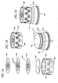
- FIG. 3A-3D A cross section of the pedestal 100 according to one preferred embodiment of the invention is shown in Figures 3A-3D .
- the pedestal 100 comprises an upper section 102 and a lower section 104.
- the overall quartz envelope of the pedestal 100 comprises a top plate 110, an upper sidewall 112, an intermediate plate 114 ( Figures 3A-3C ), a lower sidewall 116 and a bottom plate 118. It will be appreciated that the intermediate plate 114 divides the overall quartz envelope of the pedestal 100 into two subsections, or small envelopes, which are illustrated as the upper section 102 and lower section 104.
- the bottom plate 118 is preferably provided with a flange 120 to seal against a lower surface of the support sleeve 14, shown in Figures 1 and 2 , and with legs 122 for interacting with the doorplate 50.
- An upper insulation body 130 is provided in the upper section 102, while a lower insulation body 132 is provided in the lower section 104.
- the intermediate plate 114 is preferably provided with an upper bleeding hole 117, to discharge, upon heating of the pedestal 100, expanding gas present in the upper section 102 into the lower section 104.
- the bottom plate 118 is preferably provided with a lower bleeding hole 119, to discharge expanding gas present in the lower section 104 into the area below the bottom plate 118. Accordingly, expanding gas inside the pedestal can easily discharge into a region outside the reaction space 15 via the bleeding holes 117 and 119.
- the upper section 102, the lower section 104 and the bottom plate 120 (which seals against the support sleeve 14) are preferably permanently connected with each other, such that the upper insulation body 130 and the lower insulation body 132 are sealed from the atmosphere of the reaction space 15 ( Figure 1 ).
- bleeding holes 117 and 119 are shown at particular positions in the intermediate plate 114 and the bottom plate 118, respectively, these positions are for ease of illustration only; the bleeding holes 117 and 119 may be at any position in the intermediate plate 114 and the bottom plate 118.
- both bleeding holes 117 and 119 can be placed at the centers of the intermediate plate 114 and the bottom plate 118, respectively.
- bleeding hole 117 can comprise more than one opening, as can bleeding hole 119.
- a support cylinder 200 is supported on the peripheral, unobstructed part 113 of intermediate plate 114, which is preferably provided with an orientation fixation cam 115.
- the intermediate plate 114 or at least the extreme peripheral edges 113 thereof, serves as the boat support surface of the pedestal, with the support cylinder 200 ( Figure 5 ) transferring the weight of an overlying wafer boat 300 ( Figure 5 ) to the boat support surface 113, It will be appreciated, however, that other unobstructed surfaces can provide the boat support surface of the pedestal 100 in other arrangements.
- the pedestal 100 includes a material of high thermal insulation in the upper insulation body 130 either extending above or (as illustrated in Figure 3A ) exclusively above the boat support surface 113, as well as a less insulating material in the lower insulation body 132 extending below or (as illustrated in Figure 3A ) exclusively below the boat supporting surface 113.
- the upper insulation body 130 can partly extend below the boat supporting surface 113, as shown in Figure 3B
- the lower insulation body 132 can extend partly above the boat supporting surface 113, as shown in Figure 3C .
- the pedestal 100 does not have an intermediate plate. Rather, the wafer boat support surface 113 is simply a laterally extending surface of the wall of the pedestal 100.
- the pedestal of Figure 3D is filled by only a single insulation body 132.
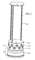
- FIG. 4 An intermediate support structure, in the form of the support cylinder 200 is shown in Figure 4 and is preferably provided with openings shown in the form of circular holes 202.
- the circular holes 202 have two purposes: first, to prevent forming a dead volume inside the cylinder 200; and second, to reduce heat conduction through the cylinder. By not making the holes 202 unduly large, these goals are advantageously achieved without seriously affecting the strength of the cylinder 200.
- the cylinder 200 is provided at its inside with three supports 210, which can support a heat shield (not shown), as discussed below with respect to Figures 5A-5C .
- the cylinder 200 is provided with a lower orientation notch 204, for mating with the orientation ridge or cam 115 of the pedestal 100 (see Figure 3 ) to ensure a fixed orientation of the cylinder 200 on top of the pedestal 100.
- the cylinder 200 is provided with an upper orientation notch 206, for mating with an orientation cam of the wafer boat 300 to ensure a fixed orientation of the wafer boat 300 on the cylinder 200.
- Figures 5A, 5B and 5C show the placement of a plurality of heat shields 230 on top of the pedestal 100.
- Figure 5A shows the support cylinder 200, provided with the large circular holes 202 and with the three supports 210 (one is visible) to support a base plate 220.
- the heat shields 230 are provided with raised parts 232 to facilitate closely spaced stacking of the heat shields 230.
- the heat shields 230 are not completely flat but comprise a few annular ripples 234 to improve their strength.
- Figure 5B shows the support cylinder 200, containing the base plate 220 and the heat shields 230, ready to be placed on top of the pedestal 100.
- Figure 5C shows the parts in an assembled state. The support cylinder 200 rests upon the boat support surface 114 of the pedestal 100, such that the cylinder 200 is now ready to receive a boat 300 ( Figure 6 ).
- Figure 6 gives another view of the pedestal 100, together with the support cylinder 200 and heat shields 230, in an assembled state. Also shown is the wafer boat 300 placed on top of the support cylinder 200.
- an upper portion 103 of the pedestal 100 including the upper section 102 and a top part of the lower section 104, has an outer diameter which is sufficiently smaller than the inner diameter of the inner process tube 12 ( Figure 1 ) so that the upper portion 103 can be accommodated inside the inner tube 12 with some clearance.
- a lower portion 105 of pedestal 100 preferably has a larger outer diameter than the upper portion 103. Preferably, this diameter is also larger than the inner diameter of the inner tube 12. In this way, heat transport by radiation along direct lines of sight from the hotter regions of the reaction space 15 ( Figure 1 ) containing the wafer boat 300 is prevented because the direct line of sight is broken.
- FIG. 2 Another advantageous feature of the preferred embodiments is illustrated in Figure 2 .
- the bottom end of the wafer boat 300 preferably practically coincides with the last winding of the heating coil 20.
- the space between the lower surface of boat 300 and the upper surface of the pedestal 100 is completely filled with the stack of closely spaced heat shields 230.
- insulation of the bottom regions of the furnace 5 begins almost immediately below the level of the heat coil 20, resulting In a very compact bottom region of the furnace 5. Consequently, the part of the furnace 5 extending below the heating coil 20 and necessary for insulation purposes can be kept very short while still providing adequate insulation.
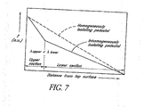
- the insulation body 130 in the upper section 102 of the pedestal 100 is made of a material with a lower thermal conductance than the material of the insulation body 132 in the lower section 104.
- the effect of this is illustrated in Figure 7 .
- a linear temperature gradient will establish itself at steady state and the heat flux through the body will be the same for every cross section of the pedestal perpendicular to the direction of heat flow.
- Changing the thermal conductivity of the insulating material in a homogeneous way will only change the heat flux but not the linear gradient; a lower thermal conductivity will result in a lower heat flux.
- the thermal conductivity upper in the upper part of the insulation body is smaller than the thermal conductivity ⁇ lower in the lower part of the insulation body, a non-linear temperature gradient will arise. Also, in this case at steady state, the heat flux through every horizontal plane will be the same. For a material with a lower thermal conductivity, a steeper temperature gradient is required to facilitate the same heat flux. Therefore, in the upper section 102 of the pedestal 100 a steeper gradient will be present than in the lower section 104. This is helpful in achieving, at the boat support surface 113 of the pedestal 100, a temperature that is sufficiently low so that the quartz envelope can carry the weight of the wafer boat 200. The higher thermal conductivity of the insulation material in the lower section 104 of the pedestal facilitates the transport of heat away from the boat support surface.
- the upper section 102 and the lower section 104 form a common quartz envelope
- the envelope of the upper section is formed of a material other than quartz.
- the envelope of the upper section can be made of SiC, for example, just as the support cylinder.
- the cylinder can be placed on top of the SiC upper section, the SiC upper section transferring the weight of the boat to a boat support surface of the lower section of the pedestal.
- the boat support surface is simply the upper surface of the lower section at which the upper section envelope interfaces with the lower section.
- the intermediate support structure is a support table, comprising support legs, rather than the illustrated cylinder.
- the upper section of the pedestal is preferably provided with cut-aways, or holes, to allow the support legs to extend down to the boat support surface of the pedestal.
- the support legs and cutaways are provided near the perimeter of the pedestal.
- Figures 3A-3C contain the intermediate plate 114 and are relatively easy to manufacture with this intermediate plate
- the upper section and lower section of the pedestal do not form two separate chambers, as illustrated by the embodiment of Figure 3D (in this case having a single insulation material 132 filling the quartz envelope).
- the bottom plate 118, sealing against the support sleeve is not an integral part of the pedestal.
- a separate bottom plate, sealing against the support sleeve, can be provided.
- the pedestal can be disposed on top of this separate bottom plate.
Description
- The invention relates to vertical furnaces for the processing of semiconductor wafers and, more particularly, to a pedestal for supporting a wafer boat in the vertical furnace.
- For high temperature processing using a wafer boat in a vertical furnace, a pedestal is commonly used at a lower end of the furnace to support the wafer boat and to provide a thermal insulation plug at the bottom of the furnace. Such a pedestal typically comprises an insulating material inside a quartz envelope, with the quartz envelope supporting the wafer boat and the insulating material providing thermal insulation. Such a pedestal is described, e.g., in
U.S. Patent No. 5,601,428 issued February 11, 1997 to Okoshi and assigned to Shin-Etsu Quartz Products Co. In that patent, the insulating material is a quartz glass foam having an apparent density of 0.1 g/cm3 to 0.8 g/cm3. - In such pedestals according to the prior art, wafer boats are supported on the top surfaces of the pedestals. For very high temperature applications, however, the top surface of the quartz pedestal is still too hot and, therefore, too weak, to serve as a support surface. To reduce the temperature of the support surface, silicon carbide (SiC) heat shields or heat shields of other suitably heat resistant material can be placed above the quartz pedestal to insulate the top surface of the underlying pedestal from the high heat of the space occupied by the wafer boat. In very high temperature ranges (e.g., 1000°C or greater), however, the heat shields can become so hot that they can act as radiation sources themselves. Therefore, their insulation value is limited and a large number of heat shields, occupying a large volume, would be required to sufficiently reduce the temperature of the top surface to make the top surface suitable for use as a wafer boat support surface.
- To address the problem of a weak wafer support surface, it is also possible to make the envelope of the pedestal of SiC instead of quartz. Such a scheme has at least two disadvantages, however. First, SiC has a thermal conductivity that is so high that the insulating function of the pedestal would be essentially nullified. Second, SiC parts are more expensive to manufacture than quartz.
- Accordingly, it is an aim of the present invention to provide a thermally insulating, wafer boat-supporting pedestal that is compact and that is capable of use in very high temperature applications in furnaces, e.g., at temperatures of 1000°C or greater.
-
EP-A-1 156 518 discloses a heat treatment apparatus comprising: a reaction vessel with a lower open end, a holding tool contained in said reaction vessel for holding a plurality of objects to be processed, and a cover for closing the lower open end of said reaction vessel, wherein an insulating unit is provided between said cover and said holding tool, said insulating unit has a heating unit, and said heating unit comprises ceramics and a heating resistor in the ceramics including a few metallic impurities. - According to one aspect of the present invention, there is provided a pedestal for insulating a lower part of a semiconductor processing furnace and for supporting an overlying wafer boat, the pedestal comprising: an envelope having a side wall, a top wall and a bottom wall, the side wall of the envelope defining an upwardly facing wafer boat support surface configured for directly or indirectly bearing a weight of the overlying wafer boat; the wafer boat support surface being below the top surface of the pedestal and
an insulation material disposed within the envelope for thermally insulating the wafer boat support surface and the lower part of the furnace, the insulation material disposed both below and above the wafer boat support surface and sealed by the envelope from gas communication with an atmosphere above the wafer boat support surface. - According to another aspect of the present invention, there is provided a method for very high temperature semiconductor processing, comprising: providing a wafer boat, the wafer boat containing a plurality of wafers; supporting the wafer boat on a surface of a pedestal according to the invention; and processing the wafers at a temperature greater than about 1000°C.
- The invention will be better understood from the detailed description of the preferred embodiments and from the appended drawings, which are meant to illustrate and not to limit the invention, and wherein:
-
Figure 1 is a cross-sectional side view of a furnace provided with a boat, a heat shield support cylinder and pedestal according to preferred embodiments of the invention; -
Figure 2 is an enlargement of a lower section ofFigure 1 ; -
Figures 3A ,3B ,3C , and3D are cross-sectional side views of the pedestal ofFigure 1 , showing various spatial relationships between the wafer boat support surface and the upper and lower sections of the pedestal; -
Figure 4 is a perspective view of the support cylinder ofFigure 1 ; -
Figures 5A, 5B and 5C are exploded, partially assembled and assembled perspective views, respectively, showing the support cylinder ofFigure 1 loaded with heat shields and placed atop the pedestal ofFigure 1 ; -
Figure 6 is a perspective view showing the assembled pedestal, support cylinder and wafer boat ofFigure 1 ; and -
Figure 7 is a graphical representation of the temperatures in the pedestal ofFigure 1 as a function of distance from the top surface, with the pedestal filled with either homogeneous or inhomogeneous insulation material. - According to preferred embodiments of the invention, a pedestal suitable for supporting a wafer boat in very high temperature applications is provided. In the illustrated embodiments, the pedestal acts as an envelope for insulating material and comprises an upper and a lower section, the lower section being below the upper section. The pedestal also has a wafer boat support surface at a level below the top, or topmost, surface of the pedestal, where the wafer boat support surface is configured to support an overlying wafer boat. The upper section at least partly extends above the boat support surface and contains an insulating material. The insulating material thermally insulates the wafer boat support surface, thereby reducing the temperature of the surface and allowing the pedestal to be used in higher temperature applications than a pedestal without the insulation provided by the upper section. In addition to the upper section, the interior volume of the pedestal as a whole is preferably substantially filled with insulating material, so that the pedestal can serve as a thermal insulation plug to thermally insulate the bottom regions of a furnace containing the pedestal from the high temperatures in upper regions of the furnace. The upper and lower sections can be completely open to one another or can be separated by an intermediate plate.
- An intermediate support structure is also provided in the illustrated embodiments. The intermediate support structure partially supports, and, more preferably, directly contacts, the overlying wafer boat and transfers the weight of that boat to the wafer support surface of the pedestal. The intermediate support structure is preferably a support cylinder. Also provided are heat shields for further insulating the wafer support surface. The heat shields can be held in a heat shield holder and are preferably placed over the top surface of the pedestal. More preferably, the heat shield holder is the intermediate support structure, e.g., the support cylinder.
- According to one preferred embodiment, the upper and lower sections are not separated by an intermediate plate and comprise a single interior volume. The material forming the surfaces, or walls, of upper and lower sections is preferably a quartz material and, more preferably, an opaque quartz material, rather than a clear quartz material. With clear quartz, although thermal conductivity is relatively low, heat transport through radiation can be substantial. With opaque quartz, heat transport by radiation is effectively prevented by the opacity of the quartz. Thus, a quartz structure preferably contains the boat support surface and serves as the boat supporting structure.
- In addition, the upper section is preferably designed such that it can accommodate an intermediate support structure. As shown in the illustrated embodiments, the support structure is preferably a support cylinder. Thus, to accommodate the support cylinder, the upper section can, for example, have a smaller diameter than either the support cylinder or lower section, in which case the support cylinder can fit around the upper section while both it and the upper section are resting on the lower section. To support the overlying wafer boat, the support cylinder preferably extends above the upper section so that the overlying wafer boat can contact it. As discussed in greater detail below, the support cylinder is preferably formed of SiC and preferably has a plurality of cut outs, e.g., through holes, in its walls in order to minimize heat transport through the cylinder.
- In another preferred embodiment, the top and lower sections of the pedestal differ from the previously discussed embodiment in that these sections are separated by an intermediate plate, forming two separate envelopes, each envelope containing insulating material. The lower section is preferably a conventional pedestal and, as such, the lower section envelope is preferably formed of quartz. The upper section can also be formed of quartz or another heat resistant material. As discussed above, the upper section preferably thermally insulates the boat support surface of the lower section. In addition, at least one opening, e.g., a plurality of holes, in the intermediate plate and in the bottom of the lower section are preferably provided to allow gas communication between the upper section and lower section and between the lower section and the ambient atmosphere below the bottom of the lower section.
- in preferred embodiments, the interiors of the upper and the lower sections of the pedestal are preferably filled with insulating material having low thermal conductivity such as, e.g., a quartz glass foam or other materials known in the art. Because open pores typically comprise a high fraction of the volume of these materials, such that exposing them to process gases is undesirable, the insulating material is preferably sealed from process gases by the upper and lower sections, which effectively serve as envelopes for these materials.
- By such an arrangement, a steep thermal gradient can be created where heat loss in the process space of the furnace is limited and does not detrimentally affect the temperature uniformity of that space. Moreover, because of the thermal gradient created in the pedestal, particularly because of a steep gradient in the upper section of the pedestal, the temperature at the level of the boat support surface is sufficiently low that the quartz is mechanically stable enough to carry the weight of a boat loaded with wafers during high temperature processing. Typically, the boat is designed to hold more than 50 and, more preferably, more than 70 wafers. In another embodiment, discussed below, on top of the pedestal, but below the wafer boat, heat shields are preferably also provided to further lower the temperature of the wafer support surface.
- in accordance with another aspect of the invention, the upper section of the pedestal is filled with an insulation material with a particularly low thermal conductivity, preferably lower that the thermal conductivity of the insulation material in the lower section of the pedestal. In this way, at steady state, a non-linear thermal gradient will exist over the pedestal, with the steepest gradient and the largest drop in temperature over the highly insulating upper section. The higher thermal conductivity of the insulating material in the lower section of the pedestal allows the heat to be transferred away from the boat support surface of the pedestal, thereby cooling that surface, while the highly insulating material in the upper section of the pedestal minimizes heat transmission to lower parts of the furnace, limiting the heat loss from the reaction space.
- In another preferred embodiment, directly on top of the pedestal is a SiC heat shield holder. The heat shield holder preferably sits directly atop the pedestal and holds a plurality of heat shields. The heat shields are stacked on top of a heat shield support plate, positioned above the top surface of the quartz pedestal, to provide for extra thermal insulation for the wafer boat support surface.
- Preferably, the heat shield holder is an intermediate support structure, such as the illustrated support cylinder. As such, the heat shields can be held in the support cylinder over the top surface of the pedestal while the support cylinder transfers the weight of the wafer boat to the wafer boat support surface of the pedestal. As such, the heat shield holder is preferably formed by a support cylinder that extends sufficiently high above the top surface of the pedestal so that a number of heat shields can be stacked inside the support cylinder. The cylinder is used to support a wafer boat on its top surface and extends downwardly to the boat support surface of the pedestal. A SiC boat can be placed on top of the support cylinder and is thus indirectly supported, via the support cylinder, on the pedestal's boat support surface. The support cylinder is made of a material that can withstand very high temperatures, such as, preferably, SiC. In the case of a support cylinder formed from SiC, the relatively high thermal conductivity of SiC will allow some extra heat transport, relative to a quartz support cylinder, to be conducted to the boat support surface of the pedestal. This heat transport is limited in the preferred embodiments, however, by providing the support cylinder with a number of through holes in the walls of the cylinder.
- Accordingly, by partly separating the insulation function and the support function of the quartz pedestal, a quartz pedestal can advantageously be used at higher temperatures than conventionally possible. For example, the pedestal can preferably be used to support wafer boats during semiconductor fabrication processes at temperatures that are preferably 1000°C or greater, more preferably, 1200°C or greater and, most preferably, 1300°C or greater. Moreover, a steeper temperature gradient allows for a more compact pedestal and a shorter overall furnace height. In addition, by using different insulating materials, with the least thermally conductive insulating material in upper parts of the pedestal, these advantages can be maximized.
- Reference will now be made to the Figures, wherein like numerals refer to like parts throughout.
-
Figure 1 shows afurnace 5 provided with apedestal 100 according to preferred embodiments of the invention. The lower section of thefurnace 5 is shown in more detail inFigure 2 . Aprocess tube 10 and aninner tube 12 are supported by asupport sleeve 14, which is in turn supported byflanges 16. A suitable support sleeve is disclosed in US Publication No.US-A-2003 0175650, filed March 15, 2002 . Thecylindrical process tube 10 is surrounded by acylindrical heating coil 20, atop heating coil 22, aninsulation material 30 and anouter shell 40. Adoorplate 50 supports apedestal 100, asupport cylinder 200 and awafer boat 300. Thepedestal 100, thesupport cylinder 200 and thewafer boat 300 can be inserted and removed from thefurnace 5 with the aid of an elevation mechanism (not shown). Thewafer boat 300 protrudes into thereaction space 15, i.e., the volume inside thefurnace 5 in which process gases can interact with wafers (not shown) during semiconductor fabrication processes. It will be appreciated that in the illustratedfurnace 5, theprocess tube 10, theinner tube 12, thesupport sleeve 14 and thepedestal 100 together delimit thereaction space 15. - A cross section of the
pedestal 100 according to one preferred embodiment of the invention is shown inFigures 3A-3D . Thepedestal 100 comprises anupper section 102 and alower section 104. The overall quartz envelope of thepedestal 100 comprises atop plate 110, anupper sidewall 112, an intermediate plate 114 (Figures 3A-3C ), alower sidewall 116 and abottom plate 118. It will be appreciated that theintermediate plate 114 divides the overall quartz envelope of thepedestal 100 into two subsections, or small envelopes, which are illustrated as theupper section 102 andlower section 104. Thebottom plate 118 is preferably provided with aflange 120 to seal against a lower surface of thesupport sleeve 14, shown inFigures 1 and2 , and withlegs 122 for interacting with thedoorplate 50. Anupper insulation body 130 is provided in theupper section 102, while alower insulation body 132 is provided in thelower section 104. - The
intermediate plate 114 is preferably provided with anupper bleeding hole 117, to discharge, upon heating of thepedestal 100, expanding gas present in theupper section 102 into thelower section 104. Similarly, thebottom plate 118 is preferably provided with alower bleeding hole 119, to discharge expanding gas present in thelower section 104 into the area below thebottom plate 118. Accordingly, expanding gas inside the pedestal can easily discharge into a region outside thereaction space 15 via the bleedingholes upper section 102, thelower section 104 and the bottom plate 120 (which seals against the support sleeve 14) are preferably permanently connected with each other, such that theupper insulation body 130 and thelower insulation body 132 are sealed from the atmosphere of the reaction space 15 (Figure 1 ). By directing gas expansion from the heated interior of thepedestal 100 to beneath the lower surface of the pedestal, which is sealed from thereaction space 15, possible contamination of process ambient of thereaction space 15 is avoided. - It will be appreciated that while the bleeding
holes intermediate plate 114 and thebottom plate 118, respectively, these positions are for ease of illustration only; the bleedingholes intermediate plate 114 and thebottom plate 118. For example, both bleedingholes intermediate plate 114 and thebottom plate 118, respectively. Moreover, it will be appreciated that bleedinghole 117 can comprise more than one opening, as can bleedinghole 119. - Still with reference to
Figures 3A-3D , in one preferred embodiment, asupport cylinder 200, described in greater detail below with respect toFigure 4 , is supported on the peripheral,unobstructed part 113 ofintermediate plate 114, which is preferably provided with anorientation fixation cam 115. Accordingly, in the illustrated embodiment, theintermediate plate 114, or at least the extremeperipheral edges 113 thereof, serves as the boat support surface of the pedestal, with the support cylinder 200 (Figure 5 ) transferring the weight of an overlying wafer boat 300 (Figure 5 ) to theboat support surface 113, It will be appreciated, however, that other unobstructed surfaces can provide the boat support surface of thepedestal 100 in other arrangements. - Preferably, the
pedestal 100 includes a material of high thermal insulation in theupper insulation body 130 either extending above or (as illustrated inFigure 3A ) exclusively above theboat support surface 113, as well as a less insulating material in thelower insulation body 132 extending below or (as illustrated inFigure 3A ) exclusively below theboat supporting surface 113. In other embodiments, however, it will be appreciated that theupper insulation body 130 can partly extend below theboat supporting surface 113, as shown inFigure 3B , or thelower insulation body 132 can extend partly above theboat supporting surface 113, as shown inFigure 3C . InFigure 3D , thepedestal 100 does not have an intermediate plate. Rather, the waferboat support surface 113 is simply a laterally extending surface of the wall of thepedestal 100. Furthermore, the pedestal ofFigure 3D is filled by only asingle insulation body 132. - An intermediate support structure, in the form of the
support cylinder 200 is shown inFigure 4 and is preferably provided with openings shown in the form ofcircular holes 202. Thecircular holes 202 have two purposes: first, to prevent forming a dead volume inside thecylinder 200; and second, to reduce heat conduction through the cylinder. By not making theholes 202 unduly large, these goals are advantageously achieved without seriously affecting the strength of thecylinder 200. Thecylinder 200 is provided at its inside with threesupports 210, which can support a heat shield (not shown), as discussed below with respect toFigures 5A-5C . At its bottom end, thecylinder 200 is provided with alower orientation notch 204, for mating with the orientation ridge orcam 115 of the pedestal 100 (seeFigure 3 ) to ensure a fixed orientation of thecylinder 200 on top of thepedestal 100. At its upper end, thecylinder 200 is provided with anupper orientation notch 206, for mating with an orientation cam of thewafer boat 300 to ensure a fixed orientation of thewafer boat 300 on thecylinder 200. -
Figures 5A, 5B and 5C show the placement of a plurality ofheat shields 230 on top of thepedestal 100.Figure 5A shows thesupport cylinder 200, provided with the largecircular holes 202 and with the three supports 210 (one is visible) to support abase plate 220. Theheat shields 230 are provided with raisedparts 232 to facilitate closely spaced stacking of the heat shields 230. Theheat shields 230 are not completely flat but comprise a fewannular ripples 234 to improve their strength.Figure 5B shows thesupport cylinder 200, containing thebase plate 220 and theheat shields 230, ready to be placed on top of thepedestal 100.Figure 5C shows the parts in an assembled state. Thesupport cylinder 200 rests upon theboat support surface 114 of thepedestal 100, such that thecylinder 200 is now ready to receive a boat 300 (Figure 6 ). -
Figure 6 gives another view of thepedestal 100, together with thesupport cylinder 200 andheat shields 230, in an assembled state. Also shown is thewafer boat 300 placed on top of thesupport cylinder 200. - Referring back to
Figures 2 and3A , an upper portion 103 of thepedestal 100, including theupper section 102 and a top part of thelower section 104, has an outer diameter which is sufficiently smaller than the inner diameter of the inner process tube 12 (Figure 1 ) so that the upper portion 103 can be accommodated inside theinner tube 12 with some clearance. Alower portion 105 ofpedestal 100, however, preferably has a larger outer diameter than the upper portion 103. Preferably, this diameter is also larger than the inner diameter of theinner tube 12. In this way, heat transport by radiation along direct lines of sight from the hotter regions of the reaction space 15 (Figure 1 ) containing thewafer boat 300 is prevented because the direct line of sight is broken. In order to accommodate thelarger diameter portion 105 of thepedestal 100, the diameter of a corresponding portion of thesupport sleeve 14 is also increased. As discussed above, a suitable support sleeve is disclosed in US Application Publication No.US-A-2003 0175650, filed March 15, 2002 . - Another advantageous feature of the preferred embodiments is illustrated in
Figure 2 . The bottom end of thewafer boat 300 preferably practically coincides with the last winding of theheating coil 20. The space between the lower surface ofboat 300 and the upper surface of thepedestal 100 is completely filled with the stack of closely spacedheat shields 230. By placing the top of theheat shields 230 nearly immediately below theheat coil 20, insulation of the bottom regions of thefurnace 5 begins almost immediately below the level of theheat coil 20, resulting In a very compact bottom region of thefurnace 5. Consequently, the part of thefurnace 5 extending below theheating coil 20 and necessary for insulation purposes can be kept very short while still providing adequate insulation. - In one preferred embodiment, the
insulation body 130 in theupper section 102 of thepedestal 100 is made of a material with a lower thermal conductance than the material of theinsulation body 132 in thelower section 104. The effect of this is illustrated inFigure 7 . For a homogeneous body of insulating material, a linear temperature gradient will establish itself at steady state and the heat flux through the body will be the same for every cross section of the pedestal perpendicular to the direction of heat flow. Changing the thermal conductivity of the insulating material in a homogeneous way will only change the heat flux but not the linear gradient; a lower thermal conductivity will result in a lower heat flux. However, if the thermal conductivity upper in the upper part of the insulation body is smaller than the thermal conductivity λlower in the lower part of the insulation body, a non-linear temperature gradient will arise. Also, in this case at steady state, the heat flux through every horizontal plane will be the same. For a material with a lower thermal conductivity, a steeper temperature gradient is required to facilitate the same heat flux. Therefore, in theupper section 102 of the pedestal 100 a steeper gradient will be present than in thelower section 104. This is helpful in achieving, at theboat support surface 113 of thepedestal 100, a temperature that is sufficiently low so that the quartz envelope can carry the weight of thewafer boat 200. The higher thermal conductivity of the insulation material in thelower section 104 of the pedestal facilitates the transport of heat away from the boat support surface. - Although in illustrated embodiments the
upper section 102 and thelower section 104 form a common quartz envelope, other variations are possible in other embodiments. For example, it is possible to use a pedestal with an upper section that is removably placed on top of the lower section. Furthermore, it is possible that the envelope of the upper section is formed of a material other than quartz. For example, the envelope of the upper section can be made of SiC, for example, just as the support cylinder. In such an embodiment, there is no longer a need for the SiC support cylinder that holds the radiation heat shields to extend downwardly to the boat support surface. Instead, the cylinder can be placed on top of the SiC upper section, the SiC upper section transferring the weight of the boat to a boat support surface of the lower section of the pedestal. In this case, the boat support surface is simply the upper surface of the lower section at which the upper section envelope interfaces with the lower section. - Although the illustrated preferred embodiments are shown with particular features, it will be clear that the present teachings do not require that embodiments of the invention possess all the illustrated features. It is, for example, possible for the intermediate support structure to be a support table, comprising support legs, rather than the illustrated cylinder. In that case, the upper section of the pedestal is preferably provided with cut-aways, or holes, to allow the support legs to extend down to the boat support surface of the pedestal. Preferably, the support legs and cutaways are provided near the perimeter of the pedestal. Furthermore, although
Figures 3A-3C contain theintermediate plate 114 and are relatively easy to manufacture with this intermediate plate, in alternative embodiments the upper section and lower section of the pedestal do not form two separate chambers, as illustrated by the embodiment ofFigure 3D (in this case having asingle insulation material 132 filling the quartz envelope). In another alternative embodiment, thebottom plate 118, sealing against the support sleeve, is not an integral part of the pedestal. A separate bottom plate, sealing against the support sleeve, can be provided. In this embodiment, the pedestal can be disposed on top of this separate bottom plate. - Similarly, various other modifications, omissions and additions may be made to the methods and structures described above without departing from the scope of the invention. All such modifications and changes are intended to fall within the scope of the invention, as defined by the appended claims.
Claims (30)
- A pedestal (100) for insulating a lower part of a semiconductor processing furnace and for supporting an overlying wafer boat, the pedestal comprising:an envelope having a side wall (114, 116), a top wall and a bottom wall, the side wall of the envelope defining an upwardly facing wafer boat support surface (113) configured for directly orindirectly bearing a weight of the overlying wafer boat; the wafer boat support surface (113) being below the top surface (110) of the pedestal (100) andan insulation material (130, 132) disposed within the envelope for thermally insulating the wafer boat support surface and the lower part of the furnace, the insulation material disposed both below and above the wafer boat support surface and sealed by the envelope from gas communication with an atmosphere above the wafer boat support surface.
- The pedestal of claim 1, wherein the insulation material comprises a single material substantially occupying an interior of the pedestal.
- The pedestal of claim 1 or 2, wherein the pedestal has an upper section (102) and a lower section (104), wherein the upper section has an upper section diameter and the lower section has a lower section diameter, wherein the lower section diameter is greater than the upper section diameter.
- The pedestal of claim 3, wherein the boat support surface extends laterally beyond the upper section diameter.
- The pedestal of any one of claims 1 to 4, wherein the insulation material comprises a first insulation material (130) disposed in an upper section of the pedestal (102) and a second insulation material (132) disposed in a lower section (104) of the pedestal.
- The pedestal of claim 5, wherein the upper and lower sections of the pedestal are surrounded by a common, integral envelope.
- The pedestal of claim 5 or 6, wherein the first insulation material has a lower thermal conductance than the second insulation material.
- The pedestal of any one of claims 5 to 7, wherein an intermediate plate (114) separates the upper section and the lower section.
- The pedestal of claim 8, wherein the intermediate plate is below the boat support surface.
- The pedestal of claim 8 or 9, wherein the upper section and the lower section are permanently joined.
- The pedestal of any one of claims 8 to 10, wherein the intermediate plate is provided with at least one upper section opening (117) for communicating gases between an upper section interior and a lower section interior.
- The pedestal of claim 11, wherein a bottom surface of the envelope is provided with at least one lower section opening (119) for communicating gases between the lower section interior and a lower ambient atmosphere under the bottom surface.
- The pedestal of any one of claims 8 to 12, wherein lower section surfaces defining the lower section comprise quartz material and upper section surfaces defining the upper section comprise a heat resistant material.
- The pedestal of claim 13, wherein the heat resistant material comprises quartz.
- The pedestal of claim 14, wherein the heat resistant material comprises opaque quartz.
- The pedestal of claim 13, wherein the heat resistant material comprises silicon carbide.
- The pedestal of claim 16, wherein the boat support surface is located at a peripheral edge of the intermediate plate.
- The pedestal of any one of claims 1 to 17, configured to receive an intermediate support structure configured to receive the overlying wafer boat, wherein the intermediate support structure sits atop the boat support surface, the intermediate support structure extending higher than a top surface of the pedestal.
- The pedestal of claim 18, wherein the intermediate support structure is a circular support cylinder (200).
- The pedestal of claim 18 or 19, wherein the support cylinder comprises silicon carbide.
- The pedestal of claim 20, wherein a wall defining sides of the support cylinder comprises a plurality of circular holes (202).
- The pedestal of claim 20 or 21, wherein a plurality of heat shields (230) is disposed in an interior of the support cylinder, each of the heat shields comprising a circular plate.
- The pedestal of claim 22, wherein each of the heat shields comprises silicon carbide.
- The pedestal of claim 23, wherein a lower heat shield of the plurality of heat shields supports an upper heat shield of the plurality of heat shields, the upper heat shield situated directly above the lower heat shield.
- The pedestal of any one of claims 1 to 24, wherein a shape of a top view of the pedestal is circular.
- The pedestal of any one of claims 1 to 25, wherein the boat support surface is on a single plane.
- A method for very high temperature semiconductor processing, comprising:providing a wafer boat, the wafer boat containing a plurality of wafers;supporting the wafer boat on a surface of a pedestal according to any preceding claim; andprocessing the wafers at a temperature greater than about 1000°C.
- The method of claim 27, wherein supporting comprises sitting the wafer boat on a surface of an intermediate support structure and transferring a weight of the wafer boat to the boat support surface of the pedestal.
- The method of claim 28, wherein processing is performed at greater than about 1200°C.
- The method of claim 29, wherein processing is performed at greater than about 1300°C.
Applications Claiming Priority (2)
| Application Number | Priority Date | Filing Date | Title |
|---|---|---|---|
| US36512902P | 2002-03-15 | 2002-03-15 | |
| US365129P | 2002-03-15 |
Publications (3)
| Publication Number | Publication Date |
|---|---|
| EP1345255A2 EP1345255A2 (en) | 2003-09-17 |
| EP1345255A3 EP1345255A3 (en) | 2005-09-07 |
| EP1345255B1 true EP1345255B1 (en) | 2014-04-23 |
Family
ID=27766268
Family Applications (1)
| Application Number | Title | Priority Date | Filing Date |
|---|---|---|---|
| EP03251586.8A Expired - Lifetime EP1345255B1 (en) | 2002-03-15 | 2003-03-14 | Multilevel pedestal for furnace |
Country Status (3)
| Country | Link |
|---|---|
| US (1) | US6902395B2 (en) |
| EP (1) | EP1345255B1 (en) |
| JP (1) | JP4452028B2 (en) |
Families Citing this family (245)
| Publication number | Priority date | Publication date | Assignee | Title |
|---|---|---|---|---|
| US20070243317A1 (en) * | 2002-07-15 | 2007-10-18 | Du Bois Dale R | Thermal Processing System and Configurable Vertical Chamber |
| US7771563B2 (en) | 2004-11-18 | 2010-08-10 | Sumitomo Precision Products Co., Ltd. | Systems and methods for achieving isothermal batch processing of substrates used for the production of micro-electro-mechanical-systems |
| WO2006104072A1 (en) * | 2005-03-28 | 2006-10-05 | Hitachi Kokusai Electric Inc. | Heat treatment device and substrate manufacturing method |
| JP4683332B2 (en) * | 2005-12-28 | 2011-05-18 | 株式会社Ihi | Heat treatment equipment |
| US7651569B2 (en) * | 2006-02-28 | 2010-01-26 | Asm International N.V. | Pedestal for furnace |
| US20090308315A1 (en) * | 2008-06-13 | 2009-12-17 | Asm International N.V. | Semiconductor processing apparatus with improved thermal characteristics and method for providing the same |
| US9394608B2 (en) | 2009-04-06 | 2016-07-19 | Asm America, Inc. | Semiconductor processing reactor and components thereof |
| CN101969021A (en) * | 2010-08-05 | 2011-02-09 | 北京七星华创电子股份有限公司 | Heat preserving barrel and vertical type heat treatment device with same |
| US20130023129A1 (en) | 2011-07-20 | 2013-01-24 | Asm America, Inc. | Pressure transmitter for a semiconductor processing environment |
| US20130078591A1 (en) * | 2011-09-22 | 2013-03-28 | Chia Hao Chang | Anti-scald protection apparatus for air heater |
| US10714315B2 (en) | 2012-10-12 | 2020-07-14 | Asm Ip Holdings B.V. | Semiconductor reaction chamber showerhead |
| US20160376700A1 (en) | 2013-02-01 | 2016-12-29 | Asm Ip Holding B.V. | System for treatment of deposition reactor |
| US11015245B2 (en) | 2014-03-19 | 2021-05-25 | Asm Ip Holding B.V. | Gas-phase reactor and system having exhaust plenum and components thereof |
| US10858737B2 (en) | 2014-07-28 | 2020-12-08 | Asm Ip Holding B.V. | Showerhead assembly and components thereof |
| US10941490B2 (en) | 2014-10-07 | 2021-03-09 | Asm Ip Holding B.V. | Multiple temperature range susceptor, assembly, reactor and system including the susceptor, and methods of using the same |
| US10276355B2 (en) | 2015-03-12 | 2019-04-30 | Asm Ip Holding B.V. | Multi-zone reactor, system including the reactor, and method of using the same |
| US10458018B2 (en) | 2015-06-26 | 2019-10-29 | Asm Ip Holding B.V. | Structures including metal carbide material, devices including the structures, and methods of forming same |
| US10211308B2 (en) | 2015-10-21 | 2019-02-19 | Asm Ip Holding B.V. | NbMC layers |
| KR20180094087A (en) | 2015-12-18 | 2018-08-22 | 헤래우스 크바르츠글라스 게엠베하 & 컴파니 케이지 | Preparation of Silica Glass Products from Silica Granules |
| KR20180095616A (en) | 2015-12-18 | 2018-08-27 | 헤래우스 크바르츠글라스 게엠베하 & 컴파니 케이지 | Preparation of silica glass body using dew point control in melting furnace |
| US10676388B2 (en) | 2015-12-18 | 2020-06-09 | Heraeus Quarzglas Gmbh & Co. Kg | Glass fibers and pre-forms made of homogeneous quartz glass |
| JP6881776B2 (en) | 2015-12-18 | 2021-06-02 | ヘレウス クワルツグラス ゲーエムベーハー ウント コンパニー カーゲー | Preparation of opaque quartz glass body |
| JP7044454B2 (en) | 2015-12-18 | 2022-03-30 | ヘレウス クワルツグラス ゲーエムベーハー ウント コンパニー カーゲー | Preparation of carbon-doped silicon dioxide granules as an intermediate in the preparation of quartz glass |
| US11952303B2 (en) | 2015-12-18 | 2024-04-09 | Heraeus Quarzglas Gmbh & Co. Kg | Increase in silicon content in the preparation of quartz glass |
| KR20180095622A (en) | 2015-12-18 | 2018-08-27 | 헤래우스 크바르츠글라스 게엠베하 & 컴파니 케이지 | Manufacture of Silica Glass Products from Molten Crucibles Made of Refractory Metals |
| EP3390304B1 (en) | 2015-12-18 | 2023-09-13 | Heraeus Quarzglas GmbH & Co. KG | Spray granulation of silicon dioxide in the production of quartz glass |
| TW201731782A (en) | 2015-12-18 | 2017-09-16 | 何瑞斯廓格拉斯公司 | Preparation of a quartz glass body in a multi-chamber oven |
| JP6881777B2 (en) | 2015-12-18 | 2021-06-02 | ヘレウス クワルツグラス ゲーエムベーハー ウント コンパニー カーゲー | Preparation of synthetic quartz glass grains |
| US11139308B2 (en) | 2015-12-29 | 2021-10-05 | Asm Ip Holding B.V. | Atomic layer deposition of III-V compounds to form V-NAND devices |
| US10529554B2 (en) | 2016-02-19 | 2020-01-07 | Asm Ip Holding B.V. | Method for forming silicon nitride film selectively on sidewalls or flat surfaces of trenches |
| US10190213B2 (en) | 2016-04-21 | 2019-01-29 | Asm Ip Holding B.V. | Deposition of metal borides |
| US10367080B2 (en) | 2016-05-02 | 2019-07-30 | Asm Ip Holding B.V. | Method of forming a germanium oxynitride film |
| US11453943B2 (en) | 2016-05-25 | 2022-09-27 | Asm Ip Holding B.V. | Method for forming carbon-containing silicon/metal oxide or nitride film by ALD using silicon precursor and hydrocarbon precursor |
| US9859151B1 (en) | 2016-07-08 | 2018-01-02 | Asm Ip Holding B.V. | Selective film deposition method to form air gaps |
| US10612137B2 (en) | 2016-07-08 | 2020-04-07 | Asm Ip Holdings B.V. | Organic reactants for atomic layer deposition |
| KR102532607B1 (en) | 2016-07-28 | 2023-05-15 | 에이에스엠 아이피 홀딩 비.브이. | Substrate processing apparatus and method of operating the same |
| US9812320B1 (en) | 2016-07-28 | 2017-11-07 | Asm Ip Holding B.V. | Method and apparatus for filling a gap |
| US9887082B1 (en) | 2016-07-28 | 2018-02-06 | Asm Ip Holding B.V. | Method and apparatus for filling a gap |
| US10643826B2 (en) | 2016-10-26 | 2020-05-05 | Asm Ip Holdings B.V. | Methods for thermally calibrating reaction chambers |
| US11532757B2 (en) | 2016-10-27 | 2022-12-20 | Asm Ip Holding B.V. | Deposition of charge trapping layers |
| US10714350B2 (en) | 2016-11-01 | 2020-07-14 | ASM IP Holdings, B.V. | Methods for forming a transition metal niobium nitride film on a substrate by atomic layer deposition and related semiconductor device structures |
| KR102546317B1 (en) | 2016-11-15 | 2023-06-21 | 에이에스엠 아이피 홀딩 비.브이. | Gas supply unit and substrate processing apparatus including the same |
| KR20180068582A (en) | 2016-12-14 | 2018-06-22 | 에이에스엠 아이피 홀딩 비.브이. | Substrate processing apparatus |
| US11581186B2 (en) | 2016-12-15 | 2023-02-14 | Asm Ip Holding B.V. | Sequential infiltration synthesis apparatus |
| US11447861B2 (en) | 2016-12-15 | 2022-09-20 | Asm Ip Holding B.V. | Sequential infiltration synthesis apparatus and a method of forming a patterned structure |
| KR20180070971A (en) | 2016-12-19 | 2018-06-27 | 에이에스엠 아이피 홀딩 비.브이. | Substrate processing apparatus |
| US10269558B2 (en) | 2016-12-22 | 2019-04-23 | Asm Ip Holding B.V. | Method of forming a structure on a substrate |
| US10867788B2 (en) | 2016-12-28 | 2020-12-15 | Asm Ip Holding B.V. | Method of forming a structure on a substrate |
| US11390950B2 (en) | 2017-01-10 | 2022-07-19 | Asm Ip Holding B.V. | Reactor system and method to reduce residue buildup during a film deposition process |
| US10468261B2 (en) | 2017-02-15 | 2019-11-05 | Asm Ip Holding B.V. | Methods for forming a metallic film on a substrate by cyclical deposition and related semiconductor device structures |
| US10529563B2 (en) | 2017-03-29 | 2020-01-07 | Asm Ip Holdings B.V. | Method for forming doped metal oxide films on a substrate by cyclical deposition and related semiconductor device structures |
| KR102457289B1 (en) | 2017-04-25 | 2022-10-21 | 에이에스엠 아이피 홀딩 비.브이. | Method for depositing a thin film and manufacturing a semiconductor device |
| US10770286B2 (en) | 2017-05-08 | 2020-09-08 | Asm Ip Holdings B.V. | Methods for selectively forming a silicon nitride film on a substrate and related semiconductor device structures |
| US10892156B2 (en) | 2017-05-08 | 2021-01-12 | Asm Ip Holding B.V. | Methods for forming a silicon nitride film on a substrate and related semiconductor device structures |
| US10886123B2 (en) | 2017-06-02 | 2021-01-05 | Asm Ip Holding B.V. | Methods for forming low temperature semiconductor layers and related semiconductor device structures |
| US11306395B2 (en) | 2017-06-28 | 2022-04-19 | Asm Ip Holding B.V. | Methods for depositing a transition metal nitride film on a substrate by atomic layer deposition and related deposition apparatus |
| KR20190009245A (en) | 2017-07-18 | 2019-01-28 | 에이에스엠 아이피 홀딩 비.브이. | Methods for forming a semiconductor device structure and related semiconductor device structures |
| US11374112B2 (en) | 2017-07-19 | 2022-06-28 | Asm Ip Holding B.V. | Method for depositing a group IV semiconductor and related semiconductor device structures |
| US10541333B2 (en) | 2017-07-19 | 2020-01-21 | Asm Ip Holding B.V. | Method for depositing a group IV semiconductor and related semiconductor device structures |
| US11018002B2 (en) | 2017-07-19 | 2021-05-25 | Asm Ip Holding B.V. | Method for selectively depositing a Group IV semiconductor and related semiconductor device structures |
| US10590535B2 (en) | 2017-07-26 | 2020-03-17 | Asm Ip Holdings B.V. | Chemical treatment, deposition and/or infiltration apparatus and method for using the same |
| US10692741B2 (en) | 2017-08-08 | 2020-06-23 | Asm Ip Holdings B.V. | Radiation shield |
| US10770336B2 (en) | 2017-08-08 | 2020-09-08 | Asm Ip Holding B.V. | Substrate lift mechanism and reactor including same |
| US11139191B2 (en) | 2017-08-09 | 2021-10-05 | Asm Ip Holding B.V. | Storage apparatus for storing cassettes for substrates and processing apparatus equipped therewith |
| US11769682B2 (en) | 2017-08-09 | 2023-09-26 | Asm Ip Holding B.V. | Storage apparatus for storing cassettes for substrates and processing apparatus equipped therewith |
| US11830730B2 (en) | 2017-08-29 | 2023-11-28 | Asm Ip Holding B.V. | Layer forming method and apparatus |
| US11295980B2 (en) | 2017-08-30 | 2022-04-05 | Asm Ip Holding B.V. | Methods for depositing a molybdenum metal film over a dielectric surface of a substrate by a cyclical deposition process and related semiconductor device structures |
| KR102491945B1 (en) | 2017-08-30 | 2023-01-26 | 에이에스엠 아이피 홀딩 비.브이. | Substrate processing apparatus |
| US11056344B2 (en) | 2017-08-30 | 2021-07-06 | Asm Ip Holding B.V. | Layer forming method |
| KR102630301B1 (en) | 2017-09-21 | 2024-01-29 | 에이에스엠 아이피 홀딩 비.브이. | Method of sequential infiltration synthesis treatment of infiltrateable material and structures and devices formed using same |
| US10844484B2 (en) | 2017-09-22 | 2020-11-24 | Asm Ip Holding B.V. | Apparatus for dispensing a vapor phase reactant to a reaction chamber and related methods |
| US10658205B2 (en) | 2017-09-28 | 2020-05-19 | Asm Ip Holdings B.V. | Chemical dispensing apparatus and methods for dispensing a chemical to a reaction chamber |
| US10403504B2 (en) | 2017-10-05 | 2019-09-03 | Asm Ip Holding B.V. | Method for selectively depositing a metallic film on a substrate |
| US10923344B2 (en) | 2017-10-30 | 2021-02-16 | Asm Ip Holding B.V. | Methods for forming a semiconductor structure and related semiconductor structures |
| US10910262B2 (en) | 2017-11-16 | 2021-02-02 | Asm Ip Holding B.V. | Method of selectively depositing a capping layer structure on a semiconductor device structure |
| US11022879B2 (en) | 2017-11-24 | 2021-06-01 | Asm Ip Holding B.V. | Method of forming an enhanced unexposed photoresist layer |
| CN111344522B (en) | 2017-11-27 | 2022-04-12 | 阿斯莫Ip控股公司 | Including clean mini-environment device |
| KR102597978B1 (en) | 2017-11-27 | 2023-11-06 | 에이에스엠 아이피 홀딩 비.브이. | Storage device for storing wafer cassettes for use with batch furnaces |
| US10872771B2 (en) | 2018-01-16 | 2020-12-22 | Asm Ip Holding B. V. | Method for depositing a material film on a substrate within a reaction chamber by a cyclical deposition process and related device structures |
| TW202325889A (en) | 2018-01-19 | 2023-07-01 | 荷蘭商Asm 智慧財產控股公司 | Deposition method |
| CN111630203A (en) | 2018-01-19 | 2020-09-04 | Asm Ip私人控股有限公司 | Method for depositing gap filling layer by plasma auxiliary deposition |
| US11018047B2 (en) | 2018-01-25 | 2021-05-25 | Asm Ip Holding B.V. | Hybrid lift pin |
| USD880437S1 (en) | 2018-02-01 | 2020-04-07 | Asm Ip Holding B.V. | Gas supply plate for semiconductor manufacturing apparatus |
| US11081345B2 (en) | 2018-02-06 | 2021-08-03 | Asm Ip Holding B.V. | Method of post-deposition treatment for silicon oxide film |
| US10896820B2 (en) | 2018-02-14 | 2021-01-19 | Asm Ip Holding B.V. | Method for depositing a ruthenium-containing film on a substrate by a cyclical deposition process |
| EP3737779A1 (en) | 2018-02-14 | 2020-11-18 | ASM IP Holding B.V. | A method for depositing a ruthenium-containing film on a substrate by a cyclical deposition process |
| KR102636427B1 (en) | 2018-02-20 | 2024-02-13 | 에이에스엠 아이피 홀딩 비.브이. | Substrate processing method and apparatus |
| US10975470B2 (en) | 2018-02-23 | 2021-04-13 | Asm Ip Holding B.V. | Apparatus for detecting or monitoring for a chemical precursor in a high temperature environment |
| US11473195B2 (en) | 2018-03-01 | 2022-10-18 | Asm Ip Holding B.V. | Semiconductor processing apparatus and a method for processing a substrate |
| US11629406B2 (en) | 2018-03-09 | 2023-04-18 | Asm Ip Holding B.V. | Semiconductor processing apparatus comprising one or more pyrometers for measuring a temperature of a substrate during transfer of the substrate |
| US11114283B2 (en) | 2018-03-16 | 2021-09-07 | Asm Ip Holding B.V. | Reactor, system including the reactor, and methods of manufacturing and using same |
| KR102646467B1 (en) | 2018-03-27 | 2024-03-11 | 에이에스엠 아이피 홀딩 비.브이. | Method of forming an electrode on a substrate and a semiconductor device structure including an electrode |
| US11230766B2 (en) | 2018-03-29 | 2022-01-25 | Asm Ip Holding B.V. | Substrate processing apparatus and method |
| US11088002B2 (en) | 2018-03-29 | 2021-08-10 | Asm Ip Holding B.V. | Substrate rack and a substrate processing system and method |
| KR102501472B1 (en) | 2018-03-30 | 2023-02-20 | 에이에스엠 아이피 홀딩 비.브이. | Substrate processing method |
| TW202344708A (en) | 2018-05-08 | 2023-11-16 | 荷蘭商Asm Ip私人控股有限公司 | Methods for depositing an oxide film on a substrate by a cyclical deposition process and related device structures |
| TWI816783B (en) | 2018-05-11 | 2023-10-01 | 荷蘭商Asm 智慧財產控股公司 | Methods for forming a doped metal carbide film on a substrate and related semiconductor device structures |
| KR102596988B1 (en) | 2018-05-28 | 2023-10-31 | 에이에스엠 아이피 홀딩 비.브이. | Method of processing a substrate and a device manufactured by the same |
| US11270899B2 (en) | 2018-06-04 | 2022-03-08 | Asm Ip Holding B.V. | Wafer handling chamber with moisture reduction |
| US11718913B2 (en) | 2018-06-04 | 2023-08-08 | Asm Ip Holding B.V. | Gas distribution system and reactor system including same |
| US11286562B2 (en) | 2018-06-08 | 2022-03-29 | Asm Ip Holding B.V. | Gas-phase chemical reactor and method of using same |
| KR102568797B1 (en) | 2018-06-21 | 2023-08-21 | 에이에스엠 아이피 홀딩 비.브이. | Substrate processing system |
| US10797133B2 (en) | 2018-06-21 | 2020-10-06 | Asm Ip Holding B.V. | Method for depositing a phosphorus doped silicon arsenide film and related semiconductor device structures |
| WO2020003000A1 (en) | 2018-06-27 | 2020-01-02 | Asm Ip Holding B.V. | Cyclic deposition methods for forming metal-containing material and films and structures including the metal-containing material |
| US11492703B2 (en) | 2018-06-27 | 2022-11-08 | Asm Ip Holding B.V. | Cyclic deposition methods for forming metal-containing material and films and structures including the metal-containing material |
| KR20200002519A (en) | 2018-06-29 | 2020-01-08 | 에이에스엠 아이피 홀딩 비.브이. | Method for depositing a thin film and manufacturing a semiconductor device |
| US10612136B2 (en) | 2018-06-29 | 2020-04-07 | ASM IP Holding, B.V. | Temperature-controlled flange and reactor system including same |
| US10755922B2 (en) | 2018-07-03 | 2020-08-25 | Asm Ip Holding B.V. | Method for depositing silicon-free carbon-containing film as gap-fill layer by pulse plasma-assisted deposition |
| US10388513B1 (en) | 2018-07-03 | 2019-08-20 | Asm Ip Holding B.V. | Method for depositing silicon-free carbon-containing film as gap-fill layer by pulse plasma-assisted deposition |
| CN110736345B (en) * | 2018-07-18 | 2021-01-29 | 北京北方华创微电子装备有限公司 | Process chamber and heat treatment furnace for SiC high-temperature oxidation process |
| US11053591B2 (en) | 2018-08-06 | 2021-07-06 | Asm Ip Holding B.V. | Multi-port gas injection system and reactor system including same |
| US10883175B2 (en) | 2018-08-09 | 2021-01-05 | Asm Ip Holding B.V. | Vertical furnace for processing substrates and a liner for use therein |
| US11430674B2 (en) | 2018-08-22 | 2022-08-30 | Asm Ip Holding B.V. | Sensor array, apparatus for dispensing a vapor phase reactant to a reaction chamber and related methods |
| KR20200030162A (en) | 2018-09-11 | 2020-03-20 | 에이에스엠 아이피 홀딩 비.브이. | Method for deposition of a thin film |
| US11024523B2 (en) * | 2018-09-11 | 2021-06-01 | Asm Ip Holding B.V. | Substrate processing apparatus and method |
| US11049751B2 (en) | 2018-09-14 | 2021-06-29 | Asm Ip Holding B.V. | Cassette supply system to store and handle cassettes and processing apparatus equipped therewith |
| CN110970344A (en) | 2018-10-01 | 2020-04-07 | Asm Ip控股有限公司 | Substrate holding apparatus, system including the same, and method of using the same |
| US11232963B2 (en) | 2018-10-03 | 2022-01-25 | Asm Ip Holding B.V. | Substrate processing apparatus and method |
| KR102592699B1 (en) | 2018-10-08 | 2023-10-23 | 에이에스엠 아이피 홀딩 비.브이. | Substrate support unit and apparatuses for depositing thin film and processing the substrate including the same |
| KR102605121B1 (en) | 2018-10-19 | 2023-11-23 | 에이에스엠 아이피 홀딩 비.브이. | Substrate processing apparatus and substrate processing method |
| KR102546322B1 (en) | 2018-10-19 | 2023-06-21 | 에이에스엠 아이피 홀딩 비.브이. | Substrate processing apparatus and substrate processing method |
| USD948463S1 (en) | 2018-10-24 | 2022-04-12 | Asm Ip Holding B.V. | Susceptor for semiconductor substrate supporting apparatus |
| US11087997B2 (en) | 2018-10-31 | 2021-08-10 | Asm Ip Holding B.V. | Substrate processing apparatus for processing substrates |
| KR20200051105A (en) | 2018-11-02 | 2020-05-13 | 에이에스엠 아이피 홀딩 비.브이. | Substrate support unit and substrate processing apparatus including the same |
| US11572620B2 (en) | 2018-11-06 | 2023-02-07 | Asm Ip Holding B.V. | Methods for selectively depositing an amorphous silicon film on a substrate |
| US11031242B2 (en) | 2018-11-07 | 2021-06-08 | Asm Ip Holding B.V. | Methods for depositing a boron doped silicon germanium film |
| US10847366B2 (en) | 2018-11-16 | 2020-11-24 | Asm Ip Holding B.V. | Methods for depositing a transition metal chalcogenide film on a substrate by a cyclical deposition process |
| US10818758B2 (en) | 2018-11-16 | 2020-10-27 | Asm Ip Holding B.V. | Methods for forming a metal silicate film on a substrate in a reaction chamber and related semiconductor device structures |
| US11217444B2 (en) | 2018-11-30 | 2022-01-04 | Asm Ip Holding B.V. | Method for forming an ultraviolet radiation responsive metal oxide-containing film |
| KR102636428B1 (en) | 2018-12-04 | 2024-02-13 | 에이에스엠 아이피 홀딩 비.브이. | A method for cleaning a substrate processing apparatus |
| US11158513B2 (en) | 2018-12-13 | 2021-10-26 | Asm Ip Holding B.V. | Methods for forming a rhenium-containing film on a substrate by a cyclical deposition process and related semiconductor device structures |
| JP2020096183A (en) | 2018-12-14 | 2020-06-18 | エーエスエム・アイピー・ホールディング・ベー・フェー | Method of forming device structure using selective deposition of gallium nitride, and system for the same |
| TWI819180B (en) | 2019-01-17 | 2023-10-21 | 荷蘭商Asm 智慧財產控股公司 | Methods of forming a transition metal containing film on a substrate by a cyclical deposition process |
| KR20200091543A (en) | 2019-01-22 | 2020-07-31 | 에이에스엠 아이피 홀딩 비.브이. | Semiconductor processing device |
| CN111524788B (en) | 2019-02-01 | 2023-11-24 | Asm Ip私人控股有限公司 | Method for topologically selective film formation of silicon oxide |
| KR102626263B1 (en) | 2019-02-20 | 2024-01-16 | 에이에스엠 아이피 홀딩 비.브이. | Cyclical deposition method including treatment step and apparatus for same |
| KR20200102357A (en) | 2019-02-20 | 2020-08-31 | 에이에스엠 아이피 홀딩 비.브이. | Apparatus and methods for plug fill deposition in 3-d nand applications |
| TW202044325A (en) | 2019-02-20 | 2020-12-01 | 荷蘭商Asm Ip私人控股有限公司 | Method of filling a recess formed within a surface of a substrate, semiconductor structure formed according to the method, and semiconductor processing apparatus |
| TW202104632A (en) | 2019-02-20 | 2021-02-01 | 荷蘭商Asm Ip私人控股有限公司 | Cyclical deposition method and apparatus for filling a recess formed within a substrate surface |
| TW202100794A (en) | 2019-02-22 | 2021-01-01 | 荷蘭商Asm Ip私人控股有限公司 | Substrate processing apparatus and method for processing substrate |
| KR20200108242A (en) | 2019-03-08 | 2020-09-17 | 에이에스엠 아이피 홀딩 비.브이. | Method for Selective Deposition of Silicon Nitride Layer and Structure Including Selectively-Deposited Silicon Nitride Layer |
| KR20200108248A (en) | 2019-03-08 | 2020-09-17 | 에이에스엠 아이피 홀딩 비.브이. | STRUCTURE INCLUDING SiOCN LAYER AND METHOD OF FORMING SAME |
| KR20200108243A (en) | 2019-03-08 | 2020-09-17 | 에이에스엠 아이피 홀딩 비.브이. | Structure Including SiOC Layer and Method of Forming Same |
| JP2020167398A (en) | 2019-03-28 | 2020-10-08 | エーエスエム・アイピー・ホールディング・ベー・フェー | Door opener and substrate processing apparatus provided therewith |
| KR20200116855A (en) | 2019-04-01 | 2020-10-13 | 에이에스엠 아이피 홀딩 비.브이. | Method of manufacturing semiconductor device |
| KR20200123380A (en) | 2019-04-19 | 2020-10-29 | 에이에스엠 아이피 홀딩 비.브이. | Layer forming method and apparatus |
| KR20200125453A (en) | 2019-04-24 | 2020-11-04 | 에이에스엠 아이피 홀딩 비.브이. | Gas-phase reactor system and method of using same |
| KR20200130121A (en) | 2019-05-07 | 2020-11-18 | 에이에스엠 아이피 홀딩 비.브이. | Chemical source vessel with dip tube |
| KR20200130118A (en) | 2019-05-07 | 2020-11-18 | 에이에스엠 아이피 홀딩 비.브이. | Method for Reforming Amorphous Carbon Polymer Film |
| KR20200130652A (en) | 2019-05-10 | 2020-11-19 | 에이에스엠 아이피 홀딩 비.브이. | Method of depositing material onto a surface and structure formed according to the method |
| JP2020188255A (en) | 2019-05-16 | 2020-11-19 | エーエスエム アイピー ホールディング ビー.ブイ. | Wafer boat handling device, vertical batch furnace, and method |
| USD975665S1 (en) | 2019-05-17 | 2023-01-17 | Asm Ip Holding B.V. | Susceptor shaft |
| USD947913S1 (en) | 2019-05-17 | 2022-04-05 | Asm Ip Holding B.V. | Susceptor shaft |
| USD935572S1 (en) | 2019-05-24 | 2021-11-09 | Asm Ip Holding B.V. | Gas channel plate |
| USD922229S1 (en) | 2019-06-05 | 2021-06-15 | Asm Ip Holding B.V. | Device for controlling a temperature of a gas supply unit |
| KR20200141003A (en) | 2019-06-06 | 2020-12-17 | 에이에스엠 아이피 홀딩 비.브이. | Gas-phase reactor system including a gas detector |
| KR20200143254A (en) | 2019-06-11 | 2020-12-23 | 에이에스엠 아이피 홀딩 비.브이. | Method of forming an electronic structure using an reforming gas, system for performing the method, and structure formed using the method |
| USD944946S1 (en) | 2019-06-14 | 2022-03-01 | Asm Ip Holding B.V. | Shower plate |
| USD931978S1 (en) | 2019-06-27 | 2021-09-28 | Asm Ip Holding B.V. | Showerhead vacuum transport |
| KR20210005515A (en) | 2019-07-03 | 2021-01-14 | 에이에스엠 아이피 홀딩 비.브이. | Temperature control assembly for substrate processing apparatus and method of using same |
| JP2021015791A (en) | 2019-07-09 | 2021-02-12 | エーエスエム アイピー ホールディング ビー.ブイ. | Plasma device and substrate processing method using coaxial waveguide |
| CN112216646A (en) | 2019-07-10 | 2021-01-12 | Asm Ip私人控股有限公司 | Substrate supporting assembly and substrate processing device comprising same |
| KR20210010307A (en) | 2019-07-16 | 2021-01-27 | 에이에스엠 아이피 홀딩 비.브이. | Substrate processing apparatus |
| KR20210010816A (en) | 2019-07-17 | 2021-01-28 | 에이에스엠 아이피 홀딩 비.브이. | Radical assist ignition plasma system and method |
| KR20210010820A (en) | 2019-07-17 | 2021-01-28 | 에이에스엠 아이피 홀딩 비.브이. | Methods of forming silicon germanium structures |
| US11643724B2 (en) | 2019-07-18 | 2023-05-09 | Asm Ip Holding B.V. | Method of forming structures using a neutral beam |
| CN112242296A (en) | 2019-07-19 | 2021-01-19 | Asm Ip私人控股有限公司 | Method of forming topologically controlled amorphous carbon polymer films |
| CN112309843A (en) | 2019-07-29 | 2021-02-02 | Asm Ip私人控股有限公司 | Selective deposition method for achieving high dopant doping |
| CN112309899A (en) | 2019-07-30 | 2021-02-02 | Asm Ip私人控股有限公司 | Substrate processing apparatus |
| CN112309900A (en) | 2019-07-30 | 2021-02-02 | Asm Ip私人控股有限公司 | Substrate processing apparatus |
| US11587814B2 (en) | 2019-07-31 | 2023-02-21 | Asm Ip Holding B.V. | Vertical batch furnace assembly |
| US11587815B2 (en) | 2019-07-31 | 2023-02-21 | Asm Ip Holding B.V. | Vertical batch furnace assembly |
| US11227782B2 (en) | 2019-07-31 | 2022-01-18 | Asm Ip Holding B.V. | Vertical batch furnace assembly |
| KR20210018759A (en) | 2019-08-05 | 2021-02-18 | 에이에스엠 아이피 홀딩 비.브이. | Liquid level sensor for a chemical source vessel |
| USD965044S1 (en) | 2019-08-19 | 2022-09-27 | Asm Ip Holding B.V. | Susceptor shaft |
| USD965524S1 (en) | 2019-08-19 | 2022-10-04 | Asm Ip Holding B.V. | Susceptor support |
| JP2021031769A (en) | 2019-08-21 | 2021-03-01 | エーエスエム アイピー ホールディング ビー.ブイ. | Production apparatus of mixed gas of film deposition raw material and film deposition apparatus |
| USD949319S1 (en) | 2019-08-22 | 2022-04-19 | Asm Ip Holding B.V. | Exhaust duct |
| KR20210024423A (en) | 2019-08-22 | 2021-03-05 | 에이에스엠 아이피 홀딩 비.브이. | Method for forming a structure with a hole |
| USD979506S1 (en) | 2019-08-22 | 2023-02-28 | Asm Ip Holding B.V. | Insulator |
| USD940837S1 (en) | 2019-08-22 | 2022-01-11 | Asm Ip Holding B.V. | Electrode |
| USD930782S1 (en) | 2019-08-22 | 2021-09-14 | Asm Ip Holding B.V. | Gas distributor |
| US11286558B2 (en) | 2019-08-23 | 2022-03-29 | Asm Ip Holding B.V. | Methods for depositing a molybdenum nitride film on a surface of a substrate by a cyclical deposition process and related semiconductor device structures including a molybdenum nitride film |
| KR20210024420A (en) | 2019-08-23 | 2021-03-05 | 에이에스엠 아이피 홀딩 비.브이. | Method for depositing silicon oxide film having improved quality by peald using bis(diethylamino)silane |
| KR20210029090A (en) | 2019-09-04 | 2021-03-15 | 에이에스엠 아이피 홀딩 비.브이. | Methods for selective deposition using a sacrificial capping layer |
| KR20210029663A (en) | 2019-09-05 | 2021-03-16 | 에이에스엠 아이피 홀딩 비.브이. | Substrate processing apparatus |
| US11562901B2 (en) | 2019-09-25 | 2023-01-24 | Asm Ip Holding B.V. | Substrate processing method |
| CN112593212B (en) | 2019-10-02 | 2023-12-22 | Asm Ip私人控股有限公司 | Method for forming topologically selective silicon oxide film by cyclic plasma enhanced deposition process |
| TW202129060A (en) | 2019-10-08 | 2021-08-01 | 荷蘭商Asm Ip控股公司 | Substrate processing device, and substrate processing method |
| KR20210043460A (en) | 2019-10-10 | 2021-04-21 | 에이에스엠 아이피 홀딩 비.브이. | Method of forming a photoresist underlayer and structure including same |
| KR20210045930A (en) | 2019-10-16 | 2021-04-27 | 에이에스엠 아이피 홀딩 비.브이. | Method of Topology-Selective Film Formation of Silicon Oxide |
| US11637014B2 (en) | 2019-10-17 | 2023-04-25 | Asm Ip Holding B.V. | Methods for selective deposition of doped semiconductor material |
| KR20210047808A (en) | 2019-10-21 | 2021-04-30 | 에이에스엠 아이피 홀딩 비.브이. | Apparatus and methods for selectively etching films |
| US11646205B2 (en) | 2019-10-29 | 2023-05-09 | Asm Ip Holding B.V. | Methods of selectively forming n-type doped material on a surface, systems for selectively forming n-type doped material, and structures formed using same |
| KR20210054983A (en) | 2019-11-05 | 2021-05-14 | 에이에스엠 아이피 홀딩 비.브이. | Structures with doped semiconductor layers and methods and systems for forming same |
| US11501968B2 (en) | 2019-11-15 | 2022-11-15 | Asm Ip Holding B.V. | Method for providing a semiconductor device with silicon filled gaps |
| KR20210062561A (en) | 2019-11-20 | 2021-05-31 | 에이에스엠 아이피 홀딩 비.브이. | Method of depositing carbon-containing material on a surface of a substrate, structure formed using the method, and system for forming the structure |
| CN112951697A (en) | 2019-11-26 | 2021-06-11 | Asm Ip私人控股有限公司 | Substrate processing apparatus |
| KR20210065848A (en) | 2019-11-26 | 2021-06-04 | 에이에스엠 아이피 홀딩 비.브이. | Methods for selectivley forming a target film on a substrate comprising a first dielectric surface and a second metallic surface |
| CN112885692A (en) | 2019-11-29 | 2021-06-01 | Asm Ip私人控股有限公司 | Substrate processing apparatus |
| CN112885693A (en) | 2019-11-29 | 2021-06-01 | Asm Ip私人控股有限公司 | Substrate processing apparatus |
| JP2021090042A (en) | 2019-12-02 | 2021-06-10 | エーエスエム アイピー ホールディング ビー.ブイ. | Substrate processing apparatus and substrate processing method |
| KR20210070898A (en) | 2019-12-04 | 2021-06-15 | 에이에스엠 아이피 홀딩 비.브이. | Substrate processing apparatus |
| TW202125596A (en) | 2019-12-17 | 2021-07-01 | 荷蘭商Asm Ip私人控股有限公司 | Method of forming vanadium nitride layer and structure including the vanadium nitride layer |
| KR20210080214A (en) | 2019-12-19 | 2021-06-30 | 에이에스엠 아이피 홀딩 비.브이. | Methods for filling a gap feature on a substrate and related semiconductor structures |
| JP2021109175A (en) | 2020-01-06 | 2021-08-02 | エーエスエム・アイピー・ホールディング・ベー・フェー | Gas supply assembly, components thereof, and reactor system including the same |
| KR20210095050A (en) | 2020-01-20 | 2021-07-30 | 에이에스엠 아이피 홀딩 비.브이. | Method of forming thin film and method of modifying surface of thin film |
| TW202130846A (en) | 2020-02-03 | 2021-08-16 | 荷蘭商Asm Ip私人控股有限公司 | Method of forming structures including a vanadium or indium layer |
| TW202146882A (en) | 2020-02-04 | 2021-12-16 | 荷蘭商Asm Ip私人控股有限公司 | Method of verifying an article, apparatus for verifying an article, and system for verifying a reaction chamber |
| US11776846B2 (en) | 2020-02-07 | 2023-10-03 | Asm Ip Holding B.V. | Methods for depositing gap filling fluids and related systems and devices |
| US11781243B2 (en) | 2020-02-17 | 2023-10-10 | Asm Ip Holding B.V. | Method for depositing low temperature phosphorous-doped silicon |
| KR20210116240A (en) | 2020-03-11 | 2021-09-27 | 에이에스엠 아이피 홀딩 비.브이. | Substrate handling device with adjustable joints |
| US11876356B2 (en) | 2020-03-11 | 2024-01-16 | Asm Ip Holding B.V. | Lockout tagout assembly and system and method of using same |
| KR20210117157A (en) | 2020-03-12 | 2021-09-28 | 에이에스엠 아이피 홀딩 비.브이. | Method for Fabricating Layer Structure Having Target Topological Profile |
| KR20210124042A (en) | 2020-04-02 | 2021-10-14 | 에이에스엠 아이피 홀딩 비.브이. | Thin film forming method |
| TW202146689A (en) | 2020-04-03 | 2021-12-16 | 荷蘭商Asm Ip控股公司 | Method for forming barrier layer and method for manufacturing semiconductor device |
| TW202145344A (en) | 2020-04-08 | 2021-12-01 | 荷蘭商Asm Ip私人控股有限公司 | Apparatus and methods for selectively etching silcon oxide films |
| US11821078B2 (en) | 2020-04-15 | 2023-11-21 | Asm Ip Holding B.V. | Method for forming precoat film and method for forming silicon-containing film |
| KR20210132600A (en) | 2020-04-24 | 2021-11-04 | 에이에스엠 아이피 홀딩 비.브이. | Methods and systems for depositing a layer comprising vanadium, nitrogen, and a further element |
| KR20210132605A (en) | 2020-04-24 | 2021-11-04 | 에이에스엠 아이피 홀딩 비.브이. | Vertical batch furnace assembly comprising a cooling gas supply |
| US11898243B2 (en) | 2020-04-24 | 2024-02-13 | Asm Ip Holding B.V. | Method of forming vanadium nitride-containing layer |
| KR20210134226A (en) | 2020-04-29 | 2021-11-09 | 에이에스엠 아이피 홀딩 비.브이. | Solid source precursor vessel |
| KR20210134869A (en) | 2020-05-01 | 2021-11-11 | 에이에스엠 아이피 홀딩 비.브이. | Fast FOUP swapping with a FOUP handler |
| KR20210141379A (en) | 2020-05-13 | 2021-11-23 | 에이에스엠 아이피 홀딩 비.브이. | Laser alignment fixture for a reactor system |
| KR20210143653A (en) | 2020-05-19 | 2021-11-29 | 에이에스엠 아이피 홀딩 비.브이. | Substrate processing apparatus |
| KR20210145078A (en) | 2020-05-21 | 2021-12-01 | 에이에스엠 아이피 홀딩 비.브이. | Structures including multiple carbon layers and methods of forming and using same |
| TW202201602A (en) | 2020-05-29 | 2022-01-01 | 荷蘭商Asm Ip私人控股有限公司 | Substrate processing device |
| TW202218133A (en) | 2020-06-24 | 2022-05-01 | 荷蘭商Asm Ip私人控股有限公司 | Method for forming a layer provided with silicon |
| TW202217953A (en) | 2020-06-30 | 2022-05-01 | 荷蘭商Asm Ip私人控股有限公司 | Substrate processing method |
| TW202219628A (en) | 2020-07-17 | 2022-05-16 | 荷蘭商Asm Ip私人控股有限公司 | Structures and methods for use in photolithography |
| TW202204662A (en) | 2020-07-20 | 2022-02-01 | 荷蘭商Asm Ip私人控股有限公司 | Method and system for depositing molybdenum layers |
| KR20220027026A (en) | 2020-08-26 | 2022-03-07 | 에이에스엠 아이피 홀딩 비.브이. | Method and system for forming metal silicon oxide and metal silicon oxynitride |
| USD990534S1 (en) | 2020-09-11 | 2023-06-27 | Asm Ip Holding B.V. | Weighted lift pin |
| USD1012873S1 (en) | 2020-09-24 | 2024-01-30 | Asm Ip Holding B.V. | Electrode for semiconductor processing apparatus |
| TW202229613A (en) | 2020-10-14 | 2022-08-01 | 荷蘭商Asm Ip私人控股有限公司 | Method of depositing material on stepped structure |
| KR20220053482A (en) | 2020-10-22 | 2022-04-29 | 에이에스엠 아이피 홀딩 비.브이. | Method of depositing vanadium metal, structure, device and a deposition assembly |
| TW202223136A (en) | 2020-10-28 | 2022-06-16 | 荷蘭商Asm Ip私人控股有限公司 | Method for forming layer on substrate, and semiconductor processing system |
| TW202235675A (en) | 2020-11-30 | 2022-09-16 | 荷蘭商Asm Ip私人控股有限公司 | Injector, and substrate processing apparatus |
| US11946137B2 (en) | 2020-12-16 | 2024-04-02 | Asm Ip Holding B.V. | Runout and wobble measurement fixtures |
| TW202231903A (en) | 2020-12-22 | 2022-08-16 | 荷蘭商Asm Ip私人控股有限公司 | Transition metal deposition method, transition metal layer, and deposition assembly for depositing transition metal on substrate |
| USD980814S1 (en) | 2021-05-11 | 2023-03-14 | Asm Ip Holding B.V. | Gas distributor for substrate processing apparatus |
| USD1023959S1 (en) | 2021-05-11 | 2024-04-23 | Asm Ip Holding B.V. | Electrode for substrate processing apparatus |
| USD981973S1 (en) | 2021-05-11 | 2023-03-28 | Asm Ip Holding B.V. | Reactor wall for substrate processing apparatus |
| USD980813S1 (en) | 2021-05-11 | 2023-03-14 | Asm Ip Holding B.V. | Gas flow control plate for substrate processing apparatus |
| USD990441S1 (en) | 2021-09-07 | 2023-06-27 | Asm Ip Holding B.V. | Gas flow control plate |
Family Cites Families (14)
| Publication number | Priority date | Publication date | Assignee | Title |
|---|---|---|---|---|
| DE3906075A1 (en) * | 1989-02-27 | 1990-08-30 | Soehlbrand Heinrich Dr Dipl Ch | METHOD FOR THERMALLY TREATING SEMICONDUCTOR MATERIALS AND DEVICE FOR CARRYING OUT THE SAME |
| US5127365A (en) * | 1990-02-27 | 1992-07-07 | Kabushiki Kaisha Toshiba | Vertical heat-treatment apparatus for semiconductor parts |
| US5308955A (en) * | 1991-07-11 | 1994-05-03 | Tokyo Electron Sagami Kabushiki Kaisha | Vertical heat treatment apparatus with vented heat insulation cover means |
| JP3230836B2 (en) * | 1992-04-09 | 2001-11-19 | 東京エレクトロン株式会社 | Heat treatment equipment |
| DE69221152T2 (en) | 1992-05-15 | 1998-02-19 | Shinetsu Quartz Prod | VERTICAL HEAT TREATMENT DEVICE AND HEAT INSULATION MATERIAL |
| JP3164248B2 (en) * | 1992-06-11 | 2001-05-08 | 東京エレクトロン株式会社 | Heat treatment equipment |
| US5252062A (en) * | 1992-10-15 | 1993-10-12 | International Business Machines Corporation | Thermal processing furnace |
| US5458688A (en) * | 1993-03-09 | 1995-10-17 | Tokyo Electron Kabushiki Kaisha | Heat treatment boat |
| US5662470A (en) * | 1995-03-31 | 1997-09-02 | Asm International N.V. | Vertical furnace |
| US5755570A (en) * | 1995-05-26 | 1998-05-26 | International Business Machines Corporation | Apparatus for in situ environment sensitive sealing and/or product controlling |
| US5846073A (en) * | 1997-03-07 | 1998-12-08 | Semitool, Inc. | Semiconductor furnace processing vessel base |
| US6191388B1 (en) * | 1998-11-18 | 2001-02-20 | Semitool, Inc. | Thermal processor and components thereof |
| JP3598032B2 (en) | 1999-11-30 | 2004-12-08 | 東京エレクトロン株式会社 | Vertical heat treatment apparatus, heat treatment method, and heat insulation unit |
| US6563686B2 (en) * | 2001-03-19 | 2003-05-13 | Applied Materials, Inc. | Pedestal assembly with enhanced thermal conductivity |
-
2003
- 2003-03-13 US US10/390,505 patent/US6902395B2/en not_active Expired - Lifetime
- 2003-03-14 EP EP03251586.8A patent/EP1345255B1/en not_active Expired - Lifetime
- 2003-03-17 JP JP2003071685A patent/JP4452028B2/en not_active Expired - Lifetime
Also Published As
| Publication number | Publication date |
|---|---|
| EP1345255A2 (en) | 2003-09-17 |
| JP2004119957A (en) | 2004-04-15 |
| EP1345255A3 (en) | 2005-09-07 |
| US6902395B2 (en) | 2005-06-07 |
| US20030175649A1 (en) | 2003-09-18 |
| JP4452028B2 (en) | 2010-04-21 |
Similar Documents
| Publication | Publication Date | Title |
|---|---|---|
| EP1345255B1 (en) | Multilevel pedestal for furnace | |
| US5709543A (en) | Vertical heat treatment apparatus | |
| US5498292A (en) | Heating device used for a gas phase growing mechanism or heat treatment mechanism | |
| EP1345254B1 (en) | Process tube support sleeve with circumferential channels | |
| KR100727014B1 (en) | Heat insulating wall, supporting structure of a heating element, heating device and substrate processing apparatus | |
| KR970003646B1 (en) | Vertical heat treatment apparatus and heat insulating material | |
| US4794220A (en) | Rotary barrel type induction vapor-phase growing apparatus | |
| US5844205A (en) | Heated substrate support structure | |
| US6344631B1 (en) | Substrate support assembly and processing apparatus | |
| KR102285296B1 (en) | Apparatus for the thermal treatment of a semiconductor substrate, especially for providing a coating | |
| TWI462185B (en) | Substrate processing apparatus, substrate supporting tool and method of manufacturing semiconductor device | |
| JP2016517167A (en) | EPI base ring | |
| KR19990087225A (en) | Heat treatment equipment | |
| US20110056434A1 (en) | Heat treatment apparatus | |
| KR100280693B1 (en) | Heat treatment equipment | |
| US6602345B1 (en) | Heater arrangement for crystal growth furnace | |
| JP5251015B2 (en) | Heat treatment apparatus and heat treatment method | |
| JPH063795B2 (en) | Heat treatment equipment for semiconductor manufacturing | |
| US6758902B2 (en) | Heater arrangement for crystal growth furnace | |
| US3648654A (en) | Vertical liquid phase crystal growth apparatus | |
| JPH06132390A (en) | Wafer boat | |
| JP4071313B2 (en) | Wafer heat treatment equipment | |
| JP7373608B1 (en) | convection suppression furnace | |
| CN112760617B (en) | Non-metal reaction chamber for chemical vapor deposition and use method thereof | |
| CN112813414B (en) | Chemical vapor deposition system |
Legal Events
| Date | Code | Title | Description |
|---|---|---|---|
| PUAI | Public reference made under article 153(3) epc to a published international application that has entered the european phase |
Free format text: ORIGINAL CODE: 0009012 |
|
| AK | Designated contracting states |
Kind code of ref document: A2 Designated state(s): AT BE BG CH CY CZ DE DK EE ES FI FR GB GR HU IE IT LI LU MC NL PT SE SI SK TR |
|
| AX | Request for extension of the european patent |
Extension state: AL LT LV MK RO |
|
| PUAL | Search report despatched |
Free format text: ORIGINAL CODE: 0009013 |
|
| AK | Designated contracting states |
Kind code of ref document: A3 Designated state(s): AT BE BG CH CY CZ DE DK EE ES FI FR GB GR HU IE IT LI LU MC NL PT SE SI SK TR |
|
| AX | Request for extension of the european patent |
Extension state: AL LT LV MK RO |
|
| RIC1 | Information provided on ipc code assigned before grant |
Ipc: 7C 23C 16/458 B Ipc: 7H 01L 21/00 A |
|
| 17P | Request for examination filed |
Effective date: 20060216 |
|
| AKX | Designation fees paid |
Designated state(s): DE FR GB NL |
|
| REG | Reference to a national code |
Ref country code: DE Ref legal event code: R079 Ref document number: 60346040 Country of ref document: DE Free format text: PREVIOUS MAIN CLASS: H01L0021000000 Ipc: H01L0021670000 |
|
| RIC1 | Information provided on ipc code assigned before grant |
Ipc: H01L 21/67 20060101AFI20130904BHEP Ipc: C23C 16/458 20060101ALI20130904BHEP |
|
| GRAP | Despatch of communication of intention to grant a patent |
Free format text: ORIGINAL CODE: EPIDOSNIGR1 |
|
| INTG | Intention to grant announced |
Effective date: 20131205 |
|
| GRAS | Grant fee paid |
Free format text: ORIGINAL CODE: EPIDOSNIGR3 |
|
| GRAA | (expected) grant |
Free format text: ORIGINAL CODE: 0009210 |
|
| AK | Designated contracting states |
Kind code of ref document: B1 Designated state(s): DE FR GB NL |
|
| REG | Reference to a national code |
Ref country code: GB Ref legal event code: FG4D |
|
| REG | Reference to a national code |
Ref country code: DE Ref legal event code: R096 Ref document number: 60346040 Country of ref document: DE Effective date: 20140528 |
|
| REG | Reference to a national code |
Ref country code: NL Ref legal event code: T3 |
|
| REG | Reference to a national code |
Ref country code: DE Ref legal event code: R097 Ref document number: 60346040 Country of ref document: DE |
|
| PLBE | No opposition filed within time limit |
Free format text: ORIGINAL CODE: 0009261 |
|
| STAA | Information on the status of an ep patent application or granted ep patent |
Free format text: STATUS: NO OPPOSITION FILED WITHIN TIME LIMIT |
|
| 26N | No opposition filed |
Effective date: 20150126 |
|
| REG | Reference to a national code |
Ref country code: DE Ref legal event code: R097 Ref document number: 60346040 Country of ref document: DE Effective date: 20150126 |
|
| REG | Reference to a national code |
Ref country code: FR Ref legal event code: PLFP Year of fee payment: 14 |
|
| REG | Reference to a national code |
Ref country code: FR Ref legal event code: PLFP Year of fee payment: 15 |
|
| PGFP | Annual fee paid to national office [announced via postgrant information from national office to epo] |
Ref country code: NL Payment date: 20170320 Year of fee payment: 15 |
|
| PGFP | Annual fee paid to national office [announced via postgrant information from national office to epo] |
Ref country code: GB Payment date: 20170308 Year of fee payment: 15 |
|
| REG | Reference to a national code |
Ref country code: FR Ref legal event code: PLFP Year of fee payment: 16 |
|
| REG | Reference to a national code |
Ref country code: NL Ref legal event code: MM Effective date: 20180401 |
|
| GBPC | Gb: european patent ceased through non-payment of renewal fee |
Effective date: 20180314 |
|
| PG25 | Lapsed in a contracting state [announced via postgrant information from national office to epo] |
Ref country code: NL Free format text: LAPSE BECAUSE OF NON-PAYMENT OF DUE FEES Effective date: 20180401 |
|
| PG25 | Lapsed in a contracting state [announced via postgrant information from national office to epo] |
Ref country code: GB Free format text: LAPSE BECAUSE OF NON-PAYMENT OF DUE FEES Effective date: 20180314 |
|
| REG | Reference to a national code |
Ref country code: DE Ref legal event code: R082 Ref document number: 60346040 Country of ref document: DE Representative=s name: D YOUNG & CO LLP, DE |
|
| PGFP | Annual fee paid to national office [announced via postgrant information from national office to epo] |
Ref country code: DE Payment date: 20220217 Year of fee payment: 20 |
|
| PGFP | Annual fee paid to national office [announced via postgrant information from national office to epo] |
Ref country code: FR Payment date: 20220221 Year of fee payment: 20 |
|
| REG | Reference to a national code |
Ref country code: DE Ref legal event code: R071 Ref document number: 60346040 Country of ref document: DE |