EP1156518A1 - Heat treating device and heat treating method - Google Patents
Heat treating device and heat treating method Download PDFInfo
- Publication number
- EP1156518A1 EP1156518A1 EP00979004A EP00979004A EP1156518A1 EP 1156518 A1 EP1156518 A1 EP 1156518A1 EP 00979004 A EP00979004 A EP 00979004A EP 00979004 A EP00979004 A EP 00979004A EP 1156518 A1 EP1156518 A1 EP 1156518A1
- Authority
- EP
- European Patent Office
- Prior art keywords
- heat treatment
- unit
- holding tool
- insulating
- insulating unit
- Prior art date
- Legal status (The legal status is an assumption and is not a legal conclusion. Google has not performed a legal analysis and makes no representation as to the accuracy of the status listed.)
- Granted
Links
Images




Classifications
-
- H—ELECTRICITY
- H10—SEMICONDUCTOR DEVICES; ELECTRIC SOLID-STATE DEVICES NOT OTHERWISE PROVIDED FOR
- H10P—GENERIC PROCESSES OR APPARATUS FOR THE MANUFACTURE OR TREATMENT OF DEVICES COVERED BY CLASS H10
- H10P72/00—Handling or holding of wafers, substrates or devices during manufacture or treatment thereof
- H10P72/04—Apparatus for manufacture or treatment
- H10P72/0431—Apparatus for thermal treatment
- H10P72/0434—Apparatus for thermal treatment mainly by convection
-
- C—CHEMISTRY; METALLURGY
- C23—COATING METALLIC MATERIAL; COATING MATERIAL WITH METALLIC MATERIAL; CHEMICAL SURFACE TREATMENT; DIFFUSION TREATMENT OF METALLIC MATERIAL; COATING BY VACUUM EVAPORATION, BY SPUTTERING, BY ION IMPLANTATION OR BY CHEMICAL VAPOUR DEPOSITION, IN GENERAL; INHIBITING CORROSION OF METALLIC MATERIAL OR INCRUSTATION IN GENERAL
- C23C—COATING METALLIC MATERIAL; COATING MATERIAL WITH METALLIC MATERIAL; SURFACE TREATMENT OF METALLIC MATERIAL BY DIFFUSION INTO THE SURFACE, BY CHEMICAL CONVERSION OR SUBSTITUTION; COATING BY VACUUM EVAPORATION, BY SPUTTERING, BY ION IMPLANTATION OR BY CHEMICAL VAPOUR DEPOSITION, IN GENERAL
- C23C16/00—Chemical coating by decomposition of gaseous compounds, without leaving reaction products of surface material in the coating, i.e. chemical vapour deposition [CVD] processes
- C23C16/44—Chemical coating by decomposition of gaseous compounds, without leaving reaction products of surface material in the coating, i.e. chemical vapour deposition [CVD] processes characterised by the method of coating
- C23C16/46—Chemical coating by decomposition of gaseous compounds, without leaving reaction products of surface material in the coating, i.e. chemical vapour deposition [CVD] processes characterised by the method of coating characterised by the method used for heating the substrate
Definitions
- the present invention relates to a heat treatment apparatus and a heat treatment method.
- a vertical heat treatment apparatus is known as one of semiconductor device manufacturing equipment.
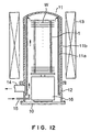
- the heat treatment apparatus is of a batch type of heat-treating many wafers in a batch and a schematic view of a device for performing the vacuum CVD method is shown in Fig. 12.
- Numeral 1 indicates a wafer boat and the wafer boat 1 holds many wafers W in the terraced state and are transferred into a reaction vessel composed of a double-structured reaction tube 11 and a cylindrical manifold 12 by an elevator not shown in the drawing.
- the reaction vessel is closed air-tightly by a cover 10.
- the reaction vessel is internally heated by a heater 13 surrounding the reaction tube 11 up to a predetermined temperature and decompressed down to predetermined pressure through an exhaust tube 14.
- Film forming gas is fed from the lower side of the reaction vessel via a gas feed tube 15, decomposed to thin film components, and deposited on the wafers W and the residual gas is lowered through the space between an inner tube 11a and an outer tube 11b from the ceiling section of the inner tube 11a and discharged through an exhaust tube 14.
- an insulating unit 16 composed of, for example, quartz fins is installed, and the atmosphere in which the wafers W are placed is insulated from the outside of the cover 10 and kept warm.
- a side wafer On the lower side of the wafer boat 1, several dummy wafers W called a side wafer are placed instead of product wafers W.
- the present invention was developed with the foregoing in view and is intended to provide a vertical heat treatment apparatus for improving the throughput.
- the present invention is a heat treatment apparatus having a reaction vessel with the lower open end, a holding tool contained in the reaction vessel for holding a plurality of objects to be processed, and a cover for blocking the opening at the lower end of the reaction vessel, wherein an insulating unit is provided between the cover and the holding tool, and the insulating unit has a heating unit, and the heating unit comprises ceramics and a heating resistor in the ceramics including few metallic impurities.
- the present invention is a heat treatment apparatus that the heating unit is arranged at least either one of the top and side of the insulating unit.
- the present invention is a heat treatment apparatus that the insulating unit comprises insulating fins positioned on a side of the heating unit side and heat insulators positioned under the insulating fins.
- the present invention is a heat treatment apparatus that the insulating unit comprises a plurality of insulating fins arranged in the horizontal direction.
- the present invention is a heat treatment apparatus that the insulating unit is fixed to the cover and the revolving shaft is connected to the holding tool, passes through the through hole of the insulating unit, and is connected to the drive unit.
- the present invention is a heat treatment apparatus that the revolving shaft comprises a first revolving shaft passing through the through hole of the insulating unit and a second revolving shaft which is connected to the first revolving shaft through a transmission unit and reaches the drive unit.
- the present invention is a heat treatment apparatus that the second revolving shaft passes through the cover and the periphery of the second revolving shaft in the insulating unit passing through the cover is enclosed by a labyrinth having a cover projection extending from the cover and a transmission projection extending from the transmission unit.
- the present invention is a heat treatment apparatus that a plurality of supports are arranged on the outer periphery of the insulating unit, at least one support is a tubular one passing through the cover, and an electric feeding line for the heating unit is arranged in the tubular support.
- the present invention is a heat treatment apparatus that the heating resistor is made of a carbon material of high purity.
- the present invention is a heat treatment apparatus that ceramics are quartz.
- the heat dissipation amount ejected from the treating atmosphere in the reaction vessel to the outside via the insulating unit is reduced, so that the treating atmosphere can be immediately stabilized at the target temperature and the treating area where the temperature is stabilized can be ensured wide.
- the insulating unit is structured so as to be fixed to the cover, the electric feed line member can be easily pulled out.
- the present invention is a heat treatment method having the steps of holding objects to be processed in a multistage manner by a holding tool, transferring the holding tool holding the objects to be processed into a reaction vessel having a lower open end from underneath, heating the inside of the reaction vessel by a heater installed outside the reaction vessel, feeding film forming gas to said reaction vessel to perform a film forming process to objects to be processed, wherein at the step of feeding film forming gas, a temperature on un under side of the holding tool is higher than that in the atmosphere where the objects to be processed are placed.
- the present invention is a heat treatment method that at the step of feeding film forming gas, film forming gas is fed from an under side of the holding tool to the above side of the holding tool and the temperature in the passing area of film forming gas on the under side of the holding tool is higher than that in the atmosphere where the objects to be processed are placed.
- the present invention is a heat treatment method that at the step of feeding film forming gas, film forming gas is fed from the above side of the holding tool to the under side of the holding tool.
- the present invention is a heat treatment method that the under side of the holding tool is heated by the insulating unit having the heating unit installed under the holding tool and a temperature on the under side of the holding tool is higher than that in the atmosphere where the objects to be processed are placed.
- the decomposition of film forming gas is promoted, so that a process of high uniformity can be performed.
- Fig. 1 is a longitudinal side view showing the whole constitution of an embodiment according to the present invention.
- Fig. 2 is a perspective view showing the appearance of the embodiment according to the present invention.
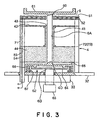
- Fig. 3 is a cross sectional view showing an insulating unit used in the embodiment according to the present invention.
- Fig. 4 is a plan view showing a heating unit incorporated in an insulating unit used in the embodiment according to the present invention.
- Fig. 5 is a characteristic diagram showing temperature changes in a treating atmosphere and a heating unit.
- Fig. 6 is a longitudinal side view showing the whole constitution of another embodiment according to the present invention.
- Fig. 7 is a side view showing another example of an insulating unit used in the present invention.
- Fig. 8 is a perspective view showing still another example of an insulating unit used in the present invention.
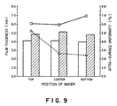
- Fig. 9 is an illustration showing the uniformity of film thickness when the device of the present invention and a conventional device are used.
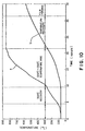
- Fig. 10 is a characteristic diagram showing results of the temperature rising speed measured for an insulating unit used in the present invention and a conventional insulating unit.
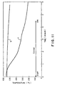
- Fig. 11 is a characteristic diagram showing results of the temperature lowering speed measured for an insulating unit used in the present invention and a conventional insulating unit.
- Fig. 12 is a longitudinal side view showing a conventional vertical heat treatment apparatus.
- Fig. 1 is a whole schematic view showing an embodiment according to the present invention, which is applied to a vertical heat treatment apparatus and Fig. 2 is a prospective view of the vertical heat treatment apparatus.
- numeral 2 indicates a double-tube structured reaction tube having an inner tube 2a and an outer tube 2b which are made of, for example, quartz and a metallic cylindrical manifold 3 is installed on the lower side of the reaction tube 2.
- a reaction vessel is composed of the reaction tube 2 and the manifold 3.
- the inner tube 2a has an open upper end and is supported by an inside portion of the manifold 3.
- the outer tube 2b has a closed upper end and its lower end is connected to the upper end of the manifold 3 air-tightly.
- the reaction vessel is composed of the inner tube 2a, the outer tube 2b, and the manifold 3.
- Numeral 31 indicates a base plate.
- a large number of, for example, 126 wafers W, which are objects to be processed, are loaded horizontally in the terraced state in a wafer board 21 (holding tool) at vertical intervals.
- the wafer boat 21, as shown in Fig. 2 is structured so that a plurality of supports 24 are installed between a top plate 22 and a bottom plate 23 and slits for holding the peripheries of the wafers W are formed in the supports 24.
- the wafer boat 21 is held on a cover 32 via an installation area of an insulating unit 4.
- the insulating unit 4 will be described later in detail.
- the cover 32 is mounted on a boat elevator 33 for transferring the wafer boat 21 in or out of the reaction tube 2 and when the elevator 33 is at the upper limit position, the cover 32 has a role to close the lower opening of the manifold 3, that is, the lower opening of the reaction vessel composed of the reaction tube 2 and the manifold 3.
- a heater 25 composed of, for example, a heating resistor is installed so as to surround the reaction tube 2.
- an insulating layer is installed around the heater 25, and a housing is additionally installed outside it.
- a heating oven 26 (Fig. 2) is composed of the heater 25, the insulating layer and the housing.
- a cooling water system for circulating cooling water around the heating oven 26 or another heating part is generally installed and a flow rate meter and an on-off valve are installed for each system line.
- a flow rate adjustable check valve (relief valve) may be installed in each circulation system.
- a plurality of gas feed tubes are installed around the manifold 3 so as to feed a plurality of processing gases (film forming gases) into the inner tube 2a.
- a gas feed tube 34 is shown and the gas feed tube 34 is connected to a gas feed source 35 via a valve Vl, a flow rate meter MFC, and a valve V2.
- An exhaust tube 36 is connected to the manifold 3 so as to exhaust gas from the space between the inner tube 2a and the outer tube 2b and the inside of the reaction tube 2 can be kept in a predetermined vacuum atmosphere by a vacuum pump 37.
- processing gas is fed into the inner tube 2a by the gas feed tube 34 from the under side of the wafer boat 2 to the above side thereof.
- the gas feed tube 34 it is possible to arrange the gas feed tube 34 above the inner tube 2a and feed processing gas from the above side of the wafer boat 21 to the under side thereof.
- the insulating unit 4 has a planar and circular heating unit 5 and a hole 50 is formed at the center of the heating unit 5.
- a shaft tube 41 for example, made of quartz is installed perpendicularly so that the inner space thereof can be aligned with the hole 50.
- a circular fin 42 which is an insulating member is installed almost horizontally via the space between the shaft tube 41 and the heating unit 5 and at the center of the fin 42, a hole 43 is formed so as to communicate with the inner space of the shaft tube 41.
- the fin 42 plays an insulating role of controlling heat dissipation from the wafer processing area to the outside and a role of reflecting radiant heat from the heating unit 5 and it is composed of, for example, opaque quartz or silicon carbide (SiC).
- a circular insulating member (insulator) 44 having a hole 40 formed at its center so as to interconnect with the inner space of the shaft tube 41 is installed so as to be supported and fixed onto the cover 32 via support members 45 (shown in Fig. 2).
- the support members 45 are positioned at intervals formed by dividing the periphery of the unit 4 into three.
- the insulating member 44 plays a roll of suppressing dissipation of heat from the above side of the insulating member 44 toward the cover 32 and the insulating member 44 may be made of, for example, a quartz block or stepwise stacked fins.
- the hole 50 of the heating unit 5, the hole 43 of the fin 42, the inner space of the shaft tube 41, and the hole 40 of the insulating member 44 form a through hole which a first revolving shaft 6A for rotating the wafer boat 21 around the perpendicular shaft passes through.
- the first revolving shaft 6A has a table 61 provided on its top and the wafer boat 21 is loaded on the table 61.
- the lower part of the first revolving shaft 6A is connected to a second revolving shaft 6B via a transmission unit 62 and the second revolving shaft 6B passes through the cover 32 air-tightly and is connected to a drive unit 63 installed to the boat elevator 33.
- the drive unit 63 is composed of, for example, a pulley connected to the revolving shaft 6B and a motor for driving the pulley via a belt.
- the transmission unit 62 has a table 64 formed at the upper end of the second revolving shaft 6B and a circular receiver 65 formed at the lower end of the first revolving shaft 6A, and a circular receiver 65 is mounted on the table 64.
- the rotation of the second revolving shaft 6B is transferred to the first rotation shaft 6A through the transmission unit 62.
- a plurality of projections (transmission projections) 66 having a comb-teeth-shaped section which are projected downward are formed and on the top of the cover 32, a plurality of projections (cover projections) 67 having a comb-teeth-shaped section which are projected upward are formed.
- the heating unit 5 has ceramics for example, quartz, and a heating resistor including few metallic impurities sealed in the ceramics.
- heater lines 52 made of a carbon material of high purity are arranged spirally, for example, in a circular plate of quartz (quartz plate) 51 having a thickness of about 8 mm. Quartz may be lay between the heater lines 52 neighboring each other and in this case, the heater lines 52 are laid between spiral quartz division walls.
- quartz quartz
- quartz supports 71, 72, 73 are installed in the periphery at three points equally divided and the supports 71 to 73 are fixed to the cover 32.
- the support 71 among the three supports 71 to 73 is composed of a tubular support and both ends of the heater line 52 are gathered, for example, at one location of the periphery of the heating unit 5.
- a pair of feeding line members connected to the heater line 52 for example, a feeding line of the same material as that of the heater line 52 passes through a thin quartz tube, and further the quartz tube passes through the tubular support (support 71), and feeding lines 53 and 54 extend outside the cover 32. Therefore, when an external power unit is connected to the feeding lines 53 and 54, the heater line 52 can generate heat.
- the two residual supports 72 and 73 may be tubular or cylindrical and are supported on the top of the cover 32.
- the treating atmosphere is increased to, for example, before or after 800°C by the heater 25, and the reaction vessel is decompressed down to a predetermined degree of vacuum by a vacuum pump 37 via the exhaust tube 36.
- the heating unit 5 of the insulating unit 4 also starts temperature rise, for example, halfway through transfer of the wafer boat 21 and raises the temperature, for example, close to 840°C which is higher than the temperature in the treating atmosphere at the time of film forming.
- the situation of each change with time of the temperature in the treating atmosphere (the temperature in the atmosphere where the wafers W are placed, which is, for example, the temperature at the height and location of the center in the arrangement area of the wafers W) and the temperature of the heating unit 5 is schematically indicated in Fig. 5 respectively by a solid line "a" and a dashed line "b".
- Fig. 5 the situation of each change with time of the temperature in the treating atmosphere (the temperature in the atmosphere where the wafers W are placed, which is, for example, the temperature at the height and location of the center in the arrangement area of the wafers W) and the temperature of the heating unit 5 is schematically indicated in Fig. 5 respectively by a solid line "a" and a dashed line "b".
- the time t1 indicates the end time of transfer (loading) of the wafer boat 21 and the time t2 indicates the point of time when the treating atmosphere reaches the target temperature.
- the heating unit 5 stands by, for example, in the neighborhood of 100°C and rises, for example, close to the target temperature 840°C from here. The points of time when the heating unit 5 and the treating atmosphere reach the respective target temperatures are almost at the same timing.
- the temperature of the heating unit 5 mentioned above is the temperature measured by a temperature sensor installed in a location at a distance of several mm from the surface of the heating unit 5.
- the reaction vessel stand by until the time t3 as a time (recovery time) for temperature stabilization without performing the process.
- the reaction vessel keeping pressure in the reaction vessel, for example, at a predetermined degree of vacuum, starts performing the process by feeding processing gas (film forming gas) composed of dichlorosilane (SiH 2 Cl 2 ) gas and nitrogen monoxide (N 2 O) gas into the reaction vessel (the reaction tube 2 and the manifold 3).
- processing gas film forming gas
- SiH 2 Cl 2 dichlorosilane
- N 2 O nitrogen monoxide
- the temperature in the neighborhood of the surface of the heating unit 5 is about 840°C, so that the periphery of the heating unit 5 and the part slightly under the heating unit 5 are higher than the temperature 800°C or so of nitrogen monoxide gas fed to the lower side of the reaction tube 2 are decomposed remarkably when they pass beside the insulating unit 4 and diffused inward the treating atmosphere in a decomposition-promoted state, and active species are deposited on the wafers W, and a silicon oxide film is formed.
- the power for the heater 25 is controlled starting from the time t4 so as to lower the temperature in the reaction vessel, and also the supply power to the heating unit 5 is reduced to 0 so as to lower the temperature of the heating unit 5, and for example, at the point of time (time t5) when the temperature in the treating atmosphere is reduced to 600°C, the wafer boat 21 is lowered.
- Fig. 6 shows a vertical heat treatment apparatus for oxidizing the silicone film on each wafer W by oxidation gas.
- the same numeral is assigned to each of the corresponding parts to those shown in Fig. 1 so as to avoid complication of numerals.
- a first point that the reaction vessel is composed of a double-tube structured reaction tube 8 composed of an inner tube 8a and an outer tube 8b without using the manifold 3
- a second point that oxidation gas, for example, oxygen gas is fed into the gap between the inner tube 8a and the outer tube 8b via a gas feed tube 81, passes through a hole 80 in the top of the inner tube 8a, and is ejected from the lower side of the inner tube 8a via an exhaust tube 82
- Numeral 83 shown in Fig. 6 indicates a uniform heat tube.
- the film quality is controlled by the moisture amount adhered to each wafer W.
- the heat capacity of the insulating unit 4 may be small, so that the surface area of the component of the insulating unit 4 may be small and the amount of moisture to be brought into the reaction vessel from the outside via the insulating unit 4 is reduced. Therefore, the film quality is improved.
- the wafers W may be subjected to the surface treatment before or during temperature rise. In this case, the amount of moisture to be brought in is little, so that the improvement of effect of the surface treatment of the wafers W can be expected.
- insulating unit 4 Other examples of the insulating unit 4 are shown in Figs. 7 and 8.
- the insulating unit 4 shown in Fig. 7 is the insulating unit 4 already mentioned that for example, fins 91 made of quartz which are an insulating member are laminated in stages under the heating unit 5.
- the insulating unit 4 shown in Fig. 8 is that not only the top but also the side are composed of a cylindrical heating unit 92.
- the cylindrical heating unit 92 can be prepared by locating, for example, the heating resistor aforementioned between the double-structure quartz tubes and sealing the upper and lower edges.
- quartz blocks or quartz fins may be arranged in the area enclosed by the cylindrical heating unit 92.
- the insulating unit 4 may be structured so as to install the heating unit 92 only on the side instead of installing the heating unit 5 on the top, or install the heating unit 5 only on the bottom, or arrange the fins as mentioned already on the top and arrange the heating unit 5 on the under side.
- a protective film may be formed, for example, by CVD or the surface may be covered with a thin protective plate.
- the material of the insulating unit 4 is not limited to quartz and it may be ceramics such as silicon carbide (SiC). Further, the present invention may be applied to a device that the wafer boat 21 is not rotated.
- a silicon oxide film was formed on a 200-mm wafer (8 inch wafer) using the vertical heat treatment apparatus shown in Fig. 1.
- a wafer boat capable of containing 126 wafers was used, and the temperature in the treating atmosphere at the time of loading the wafer boat was set to 600°C, and the temperature was increased close to 800°C, and the wafers were treated for 80 minutes aiming at a film thickness of 5.5 nm.
- As film forming gas dichlorosilane gas and nitrogen monoxide gas were fed at flow rates of 200 sccm and 400 sccm respectively and the pressure in the reaction vessel was kept at a predetermined degree of vacuum.
- the temperature in the neighborhood of the surface of the heating unit 5 of the insulating unit 4 was raised close to 840°C as explained in the embodiment aforementioned.
- each film thickness (average film thickness) of the wafers W positioned on the top, at the center, and on the bottom was checked, and the bar graphs (white blank) shown in Fig. 9 were obtained, and the intra-surface uniformity of the film thickness of the wafer W at each position was checked, and the marks ⁇ were obtained.
- the top position, center position, and bottom position mean the 6th stage, 58th stage, and 110th stage respectively counted from the uppermost stage of the wafer boat.
- films were formed on wafers W exactly in the same way except that an insulating unit composed of a conventional cylindrical body not having the heating unit shown in Fig. 12 was used, and the film thickness of each wafer W and the intra-surface uniformity were checked in the same way, and the bar graphs (oblique lines) and marks ⁇ shown in Fig. 9 were obtained.
- the intra-surface uniformity of film thickness was more than 6% in the comparison example, while the intra-surface uniformity in the present invention was about 5% in the top position and less than 3% in the center and bottom positions, and it can be understood that the device of the present invention is effective.
- the intra-surface uniformity is a value expressed by (Max - Min)/Ave ⁇ 1/2 ⁇ 200.
- a 200-mm wafer was subjected to the oxidation process using the vertical heat treatment apparatus shown in Fig. 6 and the silicon film on the surface of the wafer W was oxidized.
- the temperature in the treating atmosphere at the time of loading the wafer boat was set to 300°C, and the temperature was raised up to 850°C, and the wafer was treated for a predetermined time aiming at forming an oxide film with a thickness of 2 nm. Further, as a comparison example, the same process was performed using an insulating unit having 20 laminated quartz fins without heating unit. In each case, how wide a treating atmosphere having high temperature uniformity can be ensured was checked.
- side wafers (dummy wafers not being processed) are loaded on up to the 23rd staged from the lowest stage of the wafer boat and the film thickness uniformity of the wafer on the 24th stage from the bottom was 3.09%.
- side wafers are loaded on up to the 5th stage from the lowest stage of the wafer boat and the film thickness uniformity of the wafer was 2.88%. Therefore, according to the present invention, the number of side wafers (dummy wafers) per each batch process can be reduced.
- the intra-surface uniformity of film thickness according to the present invention can be on a level with that of the comparison example, and the treatable area (area where product wafers can be loaded) can be spread.
- the particle contamination on the wafer W was also checked and it was found that the particle contamination of the present invention was the same as that of the comparison example and particle contamination was not affected by installation of the heating unit.
- the time period from the time of loading end of the wafer boat to the time of process start was measured while stabilizing the temperature in the reaction vessel. It was found that the time period of the present invention can be shortened by about 8 minutes compared with that of the comparison example, and therefore the temperature stabilization time is shortened.
- the temperature rise condition was checked by using the same apparatus as in Example 2, and the results shown in Fig. 10 were obtained.
- Letters "a” and "b” indicate curves corresponding to the insulating unit of the present invention and the insulating unit of the comparison example respectively.
- the temperature rise of the insulating unit is fast and in the time area (recovery area) of stabilization at the target treating temperature, the temperature of the insulating unit was stable, while in the comparison example, the temperature rise of the insulating unit is slow, and even in the recovery area, the temperature rises continuously. Therefore, as a result, according to the present invention, it was found that the temperature stabilization time is shortened.
- the time period required for temperature stabilization can be shortened, so that the throughput can be improved.
Landscapes
- Chemical & Material Sciences (AREA)
- General Chemical & Material Sciences (AREA)
- Chemical Kinetics & Catalysis (AREA)
- Engineering & Computer Science (AREA)
- Materials Engineering (AREA)
- Mechanical Engineering (AREA)
- Metallurgy (AREA)
- Organic Chemistry (AREA)
- Chemical Vapour Deposition (AREA)
Abstract
Description
Claims (14)
- A heat treatment apparatus comprising:a reaction vessel with a lower open end,a holding tool contained in said reaction vessel for holding a plurality of objects to be processed, anda cover for closing the lower open end of said reaction vessel,wherein an insulating unit is provided between said cover and said holding tool,said insulating unit has a heating unit, andsaid heating unit comprises ceramics and a heating resistor in the ceramics including few metallic impurities.
- The heat treatment apparatus according to Claim 1, wherein
said heating unit is arranged at least on either of a top and a side of said insulating unit. - The heat treatment apparatus according to Claim 1, wherein
said insulating unit comprises insulating fins positioned on a side of said heating unit and heat insulators positioned under said insulating fins. - The heat treatment apparatus according to Claim 1, wherein
said insulating unit comprises a plurality of insulating fins arranged in a horizontal direction. - The heat treatment apparatus according to Claim 1, whereinsaid insulating unit is fixed to said cover anda revolving shaft is connected to said holding tool, passes through a through hole of said insulating unit, and is connected to a drive unit.
- The heat treatment apparatus according to Claim 5, wherein
said revolving shaft comprises a first revolving shaft passing through said through hole of said insulating unit and a second revolving shaft which is connected to said first revolving shaft through a transmission unit and reaches said drive unit. - The heat treatment apparatus according to Claim 6, wherein
said second revolving shaft passes through said cover and a periphery of said second revolving shaft passing through said cover is surrounded by a labyrinth having a cover projection extending from said cover and a transmission projection extending from said transmission unit. - The heat treatment apparatus according to Claim 1, whereina plurality of supports are arranged on an outer periphery of said insulating unit,at least one support is a tubular one passing through said cover, andan electric feeding line for said heating unit is arranged in said tubular support.
- The heat treatment apparatus according to Claim 1, wherein
said heating resistor is made of a carbon material having high purity. - The heat treatment apparatus according to Claim 1, wherein said ceramics are quartz.
- A heat treatment method comprising the steps of:holding objects to be processed in a multistage manner by a holding tool,transferring said holding tool holding the objects to be processed into a reaction vessel having a lower open end from underneath,heating an inside of said reaction vessel by a heater installed outside said reaction vessel, andfeeding film forming gas to said reaction vessel to perform a film forming process to objects to be processed,wherein at said step of feeding film forming gas, a temperature on an under side of said holding tool is higher than that in an atmosphere where said objects to be processed are placed.
- The heat treatment method according to Claim 11, whereinat said step of feeding film forming gas, said film forming gas is fed from an under side of said holding tool to an above side of said holding tool anda temperature in a passing area of said film forming gas on said under side of said holding tool is higher than that in said atmosphere where said objects to be processed are placed.
- The heat treatment method according to Claim 11, wherein
at said step of feeding film forming gas, said film forming gas is fed from an above side of said holding tool to said under side of said holding tool. - The heat treatment method according to Claim 11, whereinsaid under side of said holding tool is heated by an insulating unit having a heating unit installed under said holding tool anda temperature on said under side of said holding tool is higher than that in said atmosphere where said objects to be processed are placed.
Applications Claiming Priority (3)
| Application Number | Priority Date | Filing Date | Title |
|---|---|---|---|
| JP33974999A JP3598032B2 (en) | 1999-11-30 | 1999-11-30 | Vertical heat treatment apparatus, heat treatment method, and heat insulation unit |
| JP33974999 | 1999-11-30 | ||
| PCT/JP2000/008401 WO2001041202A1 (en) | 1999-11-30 | 2000-11-29 | Heat treating device and heat treating method |
Publications (3)
| Publication Number | Publication Date |
|---|---|
| EP1156518A1 true EP1156518A1 (en) | 2001-11-21 |
| EP1156518A4 EP1156518A4 (en) | 2004-10-27 |
| EP1156518B1 EP1156518B1 (en) | 2008-04-23 |
Family
ID=18330455
Family Applications (1)
| Application Number | Title | Priority Date | Filing Date |
|---|---|---|---|
| EP00979004A Expired - Lifetime EP1156518B1 (en) | 1999-11-30 | 2000-11-29 | Heat treating device and heat treating method |
Country Status (7)
| Country | Link |
|---|---|
| US (1) | US6444940B1 (en) |
| EP (1) | EP1156518B1 (en) |
| JP (1) | JP3598032B2 (en) |
| KR (2) | KR100638946B1 (en) |
| DE (1) | DE60038669T2 (en) |
| TW (1) | TW478046B (en) |
| WO (1) | WO2001041202A1 (en) |
Cited By (2)
| Publication number | Priority date | Publication date | Assignee | Title |
|---|---|---|---|---|
| EP1345255A2 (en) | 2002-03-15 | 2003-09-17 | Asm International N.V. | Multilevel pedestal for furnace |
| WO2024023326A1 (en) * | 2022-07-29 | 2024-02-01 | centrotherm international AG | Device for thermally treating substrates, in particular semiconductor wafers |
Families Citing this family (35)
| Publication number | Priority date | Publication date | Assignee | Title |
|---|---|---|---|---|
| JP3912208B2 (en) * | 2002-02-28 | 2007-05-09 | 東京エレクトロン株式会社 | Heat treatment equipment |
| JP4276813B2 (en) | 2002-03-26 | 2009-06-10 | 株式会社日立国際電気 | Heat treatment apparatus and semiconductor manufacturing method |
| WO2004013901A2 (en) * | 2002-08-02 | 2004-02-12 | Wafermasters, Inc. | Batch furnace |
| US6727194B2 (en) * | 2002-08-02 | 2004-04-27 | Wafermasters, Inc. | Wafer batch processing system and method |
| JP4523225B2 (en) | 2002-09-24 | 2010-08-11 | 東京エレクトロン株式会社 | Heat treatment equipment |
| KR100860437B1 (en) * | 2004-10-07 | 2008-09-25 | 가부시키가이샤 히다치 고쿠사이 덴키 | Substrate treating apparatus and semiconductor device manufacturing method |
| JP4820137B2 (en) * | 2005-09-26 | 2011-11-24 | 株式会社日立国際電気 | Heating element holding structure |
| JP4683332B2 (en) * | 2005-12-28 | 2011-05-18 | 株式会社Ihi | Heat treatment equipment |
| JP2007189077A (en) * | 2006-01-13 | 2007-07-26 | Ishikawajima Harima Heavy Ind Co Ltd | Heat treatment equipment |
| JP2008034463A (en) | 2006-07-26 | 2008-02-14 | Hitachi Kokusai Electric Inc | Substrate processing equipment |
| US20100133325A1 (en) * | 2008-12-01 | 2010-06-03 | Xerox Corporation | Unified metal alloying in a diffusion furnace |
| US7980447B2 (en) | 2008-12-12 | 2011-07-19 | Xerox Corporation | Jet stack brazing in a diffusion furnace |
| JP2010177653A (en) * | 2009-02-02 | 2010-08-12 | Koyo Thermo System Kk | Vertical furnace device |
| KR101041143B1 (en) * | 2009-04-16 | 2011-06-13 | 삼성모바일디스플레이주식회사 | Substrate processing equipment |
| JP2012195565A (en) * | 2011-02-28 | 2012-10-11 | Hitachi Kokusai Electric Inc | Substrate processing apparatus, substrate processing method, and manufacturing method of semiconductor device |
| US20120244684A1 (en) * | 2011-03-24 | 2012-09-27 | Kunihiko Suzuki | Film-forming apparatus and method |
| US9018567B2 (en) * | 2011-07-13 | 2015-04-28 | Asm International N.V. | Wafer processing apparatus with heated, rotating substrate support |
| CN104520975B (en) * | 2012-07-30 | 2018-07-31 | 株式会社日立国际电气 | The manufacturing method of substrate processing device and semiconductor devices |
| JP5977274B2 (en) * | 2013-03-21 | 2016-08-24 | 東京エレクトロン株式会社 | Batch type vertical substrate processing apparatus and substrate holder |
| CN105914163B (en) * | 2015-02-25 | 2020-03-24 | 株式会社国际电气 | Substrate processing apparatus, manufacturing method of semiconductor device, and heating unit |
| JP6630146B2 (en) | 2015-02-25 | 2020-01-15 | 株式会社Kokusai Electric | Substrate processing apparatus, semiconductor device manufacturing method, and heating unit |
| TWI611043B (en) * | 2015-08-04 | 2018-01-11 | 日立國際電氣股份有限公司 | Substrate processing apparatus, manufacturing method of semiconductor device, and recording medium |
| KR101724613B1 (en) * | 2016-05-02 | 2017-04-07 | (주)젠스엠 | Vertical type heat treatment apparatus |
| KR102127130B1 (en) * | 2017-02-17 | 2020-06-26 | 가부시키가이샤 코쿠사이 엘렉트릭 | Substrate processing device, manufacturing method and program of semiconductor device |
| KR20190008101A (en) * | 2017-07-14 | 2019-01-23 | 가부시키가이샤 코쿠사이 엘렉트릭 | Substrate processing apparatus, substrate retainer and method of manufacturing semiconductor device |
| US10593572B2 (en) * | 2018-03-15 | 2020-03-17 | Kokusai Electric Corporation | Substrate processing apparatus and method of manufacturing semiconductor device |
| JP6952633B2 (en) * | 2018-03-23 | 2021-10-20 | 東京エレクトロン株式会社 | Substrate heating device and substrate processing device using this |
| CN110736345B (en) * | 2018-07-18 | 2021-01-29 | 北京北方华创微电子装备有限公司 | Process chamber and heat treatment furnace for SiC high temperature oxidation process |
| US11024523B2 (en) | 2018-09-11 | 2021-06-01 | Asm Ip Holding B.V. | Substrate processing apparatus and method |
| US11232963B2 (en) * | 2018-10-03 | 2022-01-25 | Asm Ip Holding B.V. | Substrate processing apparatus and method |
| JP6890114B2 (en) | 2018-12-05 | 2021-06-18 | 株式会社Kokusai Electric | Manufacturing method of substrate processing equipment and semiconductor equipment |
| KR102485866B1 (en) * | 2018-12-17 | 2023-01-09 | 주식회사 원익아이피에스 | Apparatus for processing substrate |
| CN112254536A (en) * | 2020-10-16 | 2021-01-22 | 北京北方华创微电子装备有限公司 | Support heat preservation device and vertical furnace |
| JP7514876B2 (en) * | 2022-03-25 | 2024-07-11 | 株式会社Kokusai Electric | Substrate processing apparatus, semiconductor device manufacturing method and substrate support |
| JP7798445B2 (en) * | 2022-08-19 | 2026-01-14 | 東京エレクトロン株式会社 | Heat Treatment Equipment |
Family Cites Families (20)
| Publication number | Priority date | Publication date | Assignee | Title |
|---|---|---|---|---|
| US5198034A (en) * | 1987-03-31 | 1993-03-30 | Epsilon Technology, Inc. | Rotatable substrate supporting mechanism with temperature sensing device for use in chemical vapor deposition equipment |
| DE3855871T2 (en) * | 1987-09-11 | 1997-10-16 | Hitachi Ltd | Device for carrying out a heat treatment on semiconductor wafers |
| JP2756566B2 (en) | 1987-11-21 | 1998-05-25 | 東京エレクトロン株式会社 | Vertical heat treatment equipment |
| US5048800A (en) * | 1988-12-27 | 1991-09-17 | Kabushiki Kaisha Toshiba | Vertical heat treatment apparatus |
| JPH02218117A (en) | 1989-02-17 | 1990-08-30 | Tel Sagami Ltd | Thermal treatment apparatus |
| JPH04121731A (en) | 1990-09-12 | 1992-04-22 | Fuji Photo Film Co Ltd | Silver halide photographic sensitive material |
| JP3061635B2 (en) * | 1990-11-13 | 2000-07-10 | 東京エレクトロン株式会社 | Vertical heat treatment equipment |
| JPH05136071A (en) * | 1991-11-15 | 1993-06-01 | Hitachi Ltd | Semiconductor wafer board and diffusion cvd apparatus |
| JP3230836B2 (en) * | 1992-04-09 | 2001-11-19 | 東京エレクトロン株式会社 | Heat treatment equipment |
| US5324540A (en) * | 1992-08-17 | 1994-06-28 | Tokyo Electron Limited | System and method for supporting and rotating substrates in a process chamber |
| JP3109702B2 (en) | 1992-10-15 | 2000-11-20 | 東京エレクトロン株式会社 | Heat treatment equipment |
| US5540782A (en) | 1992-10-15 | 1996-07-30 | Tokyo Electron Kabushiki Kaisha | Heat treating apparatus having heat transmission-preventing plates |
| JPH0758036A (en) * | 1993-08-16 | 1995-03-03 | Ebara Corp | Thin film forming equipment |
| JPH0817746A (en) | 1994-06-30 | 1996-01-19 | Toshiba Mach Co Ltd | Heater |
| JPH0888192A (en) * | 1994-09-19 | 1996-04-02 | Touyoko Kagaku Kk | Vertical high speed heat treatment equipment |
| JP3471144B2 (en) * | 1995-09-06 | 2003-11-25 | 東京エレクトロン株式会社 | Vertical heat treatment apparatus, heat insulation structure thereof, and heat shield plate |
| JP3423131B2 (en) * | 1995-11-20 | 2003-07-07 | 東京エレクトロン株式会社 | Heat treatment equipment and treatment equipment |
| JP3474991B2 (en) | 1995-11-22 | 2003-12-08 | 東京エレクトロン株式会社 | Oxidation treatment apparatus and oxidation treatment method |
| KR100224659B1 (en) * | 1996-05-17 | 1999-10-15 | 윤종용 | Caps for Vertical Vapor Growth Devices |
| JP3930119B2 (en) | 1997-09-26 | 2007-06-13 | 東芝セラミックス株式会社 | Heater unit for semiconductor heat treatment equipment |
-
1999
- 1999-11-30 JP JP33974999A patent/JP3598032B2/en not_active Expired - Fee Related
-
2000
- 2000-11-29 US US09/890,328 patent/US6444940B1/en not_active Expired - Lifetime
- 2000-11-29 WO PCT/JP2000/008401 patent/WO2001041202A1/en not_active Ceased
- 2000-11-29 TW TW089125352A patent/TW478046B/en not_active IP Right Cessation
- 2000-11-29 EP EP00979004A patent/EP1156518B1/en not_active Expired - Lifetime
- 2000-11-29 DE DE60038669T patent/DE60038669T2/en not_active Expired - Lifetime
- 2000-11-29 KR KR1020017009404A patent/KR100638946B1/en not_active Expired - Fee Related
- 2000-11-29 KR KR1020067010029A patent/KR100709802B1/en not_active Expired - Fee Related
Cited By (3)
| Publication number | Priority date | Publication date | Assignee | Title |
|---|---|---|---|---|
| EP1345255A2 (en) | 2002-03-15 | 2003-09-17 | Asm International N.V. | Multilevel pedestal for furnace |
| EP1345255A3 (en) * | 2002-03-15 | 2005-09-07 | Asm International N.V. | Multilevel pedestal for furnace |
| WO2024023326A1 (en) * | 2022-07-29 | 2024-02-01 | centrotherm international AG | Device for thermally treating substrates, in particular semiconductor wafers |
Also Published As
| Publication number | Publication date |
|---|---|
| TW478046B (en) | 2002-03-01 |
| DE60038669D1 (en) | 2008-06-05 |
| KR100709802B1 (en) | 2007-04-24 |
| KR100638946B1 (en) | 2006-10-25 |
| EP1156518B1 (en) | 2008-04-23 |
| KR20010101717A (en) | 2001-11-14 |
| US6444940B1 (en) | 2002-09-03 |
| WO2001041202A1 (en) | 2001-06-07 |
| EP1156518A4 (en) | 2004-10-27 |
| JP2001156005A (en) | 2001-06-08 |
| DE60038669T2 (en) | 2009-05-28 |
| KR20060064030A (en) | 2006-06-12 |
| JP3598032B2 (en) | 2004-12-08 |
Similar Documents
| Publication | Publication Date | Title |
|---|---|---|
| US6444940B1 (en) | Heat treating device and heat treating method | |
| EP0818807B1 (en) | Dual vertical thermal processing furnace | |
| US5431561A (en) | Method and apparatus for heat treating | |
| US4745088A (en) | Vapor phase growth on semiconductor wafers | |
| JP3125199B2 (en) | Vertical heat treatment equipment | |
| EP1388891B1 (en) | System for heat treating semiconductor | |
| KR100395994B1 (en) | Supporting boat of the object to be treated | |
| JP3023982B2 (en) | Film formation method | |
| JP3184000B2 (en) | Method and apparatus for forming thin film | |
| US5567152A (en) | Heat processing apparatus | |
| JP2005123532A (en) | Film forming apparatus and film forming method | |
| US20110253049A1 (en) | Semiconductor processing apparatus | |
| US5677235A (en) | Method for forming silicon film | |
| WO2003041139A1 (en) | Thermal treating apparatus | |
| US5500388A (en) | Heat treatment process for wafers | |
| US20030221623A1 (en) | Fabricating a semiconductor device | |
| JP2819073B2 (en) | Method of forming doped thin film | |
| CN104934348A (en) | Apparatus for processing substrate | |
| US8771416B2 (en) | Substrate processing apparatus with an insulator disposed in the reaction chamber | |
| JPH05251357A (en) | Formation method of film | |
| JP4610908B2 (en) | Substrate processing apparatus and semiconductor device manufacturing method | |
| JP3081886B2 (en) | Film formation method | |
| JP2001156011A (en) | Semiconductor wafer heat treatment equipment | |
| JP2683673B2 (en) | Vertical heat treatment equipment | |
| JP2693465B2 (en) | Semiconductor wafer processing equipment |
Legal Events
| Date | Code | Title | Description |
|---|---|---|---|
| PUAI | Public reference made under article 153(3) epc to a published international application that has entered the european phase |
Free format text: ORIGINAL CODE: 0009012 |
|
| 17P | Request for examination filed |
Effective date: 20010731 |
|
| AK | Designated contracting states |
Kind code of ref document: A1 Designated state(s): AT BE CH CY DE DK ES FI FR GB GR IE IT LI LU MC NL PT SE TR |
|
| RIC1 | Information provided on ipc code assigned before grant |
Ipc: 7H 01L 21/00 B Ipc: 7H 01L 21/22 B Ipc: 7H 01L 21/31 A Ipc: 7C 23C 16/44 B Ipc: 7H 01L 21/205 B Ipc: 7C 23C 16/46 B |
|
| RBV | Designated contracting states (corrected) |
Designated state(s): DE FR GB IT NL |
|
| A4 | Supplementary search report drawn up and despatched |
Effective date: 20040908 |
|
| 17Q | First examination report despatched |
Effective date: 20050420 |
|
| GRAP | Despatch of communication of intention to grant a patent |
Free format text: ORIGINAL CODE: EPIDOSNIGR1 |
|
| GRAS | Grant fee paid |
Free format text: ORIGINAL CODE: EPIDOSNIGR3 |
|
| GRAA | (expected) grant |
Free format text: ORIGINAL CODE: 0009210 |
|
| AK | Designated contracting states |
Kind code of ref document: B1 Designated state(s): DE FR GB IT NL |
|
| REG | Reference to a national code |
Ref country code: GB Ref legal event code: FG4D |
|
| REF | Corresponds to: |
Ref document number: 60038669 Country of ref document: DE Date of ref document: 20080605 Kind code of ref document: P |
|
| ET | Fr: translation filed | ||
| PLBE | No opposition filed within time limit |
Free format text: ORIGINAL CODE: 0009261 |
|
| STAA | Information on the status of an ep patent application or granted ep patent |
Free format text: STATUS: NO OPPOSITION FILED WITHIN TIME LIMIT |
|
| 26N | No opposition filed |
Effective date: 20090126 |
|
| REG | Reference to a national code |
Ref country code: FR Ref legal event code: PLFP Year of fee payment: 16 |
|
| PGFP | Annual fee paid to national office [announced via postgrant information from national office to epo] |
Ref country code: IT Payment date: 20151124 Year of fee payment: 16 Ref country code: DE Payment date: 20151125 Year of fee payment: 16 Ref country code: GB Payment date: 20151125 Year of fee payment: 16 |
|
| PGFP | Annual fee paid to national office [announced via postgrant information from national office to epo] |
Ref country code: FR Payment date: 20151008 Year of fee payment: 16 Ref country code: NL Payment date: 20151012 Year of fee payment: 16 |
|
| REG | Reference to a national code |
Ref country code: DE Ref legal event code: R119 Ref document number: 60038669 Country of ref document: DE |
|
| REG | Reference to a national code |
Ref country code: NL Ref legal event code: MM Effective date: 20161201 |
|
| GBPC | Gb: european patent ceased through non-payment of renewal fee |
Effective date: 20161129 |
|
| REG | Reference to a national code |
Ref country code: FR Ref legal event code: ST Effective date: 20170731 |
|
| PG25 | Lapsed in a contracting state [announced via postgrant information from national office to epo] |
Ref country code: NL Free format text: LAPSE BECAUSE OF NON-PAYMENT OF DUE FEES Effective date: 20161201 |
|
| PG25 | Lapsed in a contracting state [announced via postgrant information from national office to epo] |
Ref country code: FR Free format text: LAPSE BECAUSE OF NON-PAYMENT OF DUE FEES Effective date: 20161130 Ref country code: IT Free format text: LAPSE BECAUSE OF NON-PAYMENT OF DUE FEES Effective date: 20161129 |
|
| PG25 | Lapsed in a contracting state [announced via postgrant information from national office to epo] |
Ref country code: GB Free format text: LAPSE BECAUSE OF NON-PAYMENT OF DUE FEES Effective date: 20161129 Ref country code: DE Free format text: LAPSE BECAUSE OF NON-PAYMENT OF DUE FEES Effective date: 20170601 |