EP1343232A1 - Barrette de lasers semiconducteurs à réseau latéral - Google Patents
Barrette de lasers semiconducteurs à réseau latéral Download PDFInfo
- Publication number
- EP1343232A1 EP1343232A1 EP02005165A EP02005165A EP1343232A1 EP 1343232 A1 EP1343232 A1 EP 1343232A1 EP 02005165 A EP02005165 A EP 02005165A EP 02005165 A EP02005165 A EP 02005165A EP 1343232 A1 EP1343232 A1 EP 1343232A1
- Authority
- EP
- European Patent Office
- Prior art keywords
- laser
- lattice structure
- layer
- waveguide
- ridges
- Prior art date
- Legal status (The legal status is an assumption and is not a legal conclusion. Google has not performed a legal analysis and makes no representation as to the accuracy of the status listed.)
- Granted
Links
Images

Classifications
-
- H—ELECTRICITY
- H01—ELECTRIC ELEMENTS
- H01S—DEVICES USING THE PROCESS OF LIGHT AMPLIFICATION BY STIMULATED EMISSION OF RADIATION [LASER] TO AMPLIFY OR GENERATE LIGHT; DEVICES USING STIMULATED EMISSION OF ELECTROMAGNETIC RADIATION IN WAVE RANGES OTHER THAN OPTICAL
- H01S5/00—Semiconductor lasers
- H01S5/10—Construction or shape of the optical resonator, e.g. extended or external cavity, coupled cavities, bent-guide, varying width, thickness or composition of the active region
- H01S5/12—Construction or shape of the optical resonator, e.g. extended or external cavity, coupled cavities, bent-guide, varying width, thickness or composition of the active region the resonator having a periodic structure, e.g. in distributed feedback [DFB] lasers
-
- H—ELECTRICITY
- H01—ELECTRIC ELEMENTS
- H01S—DEVICES USING THE PROCESS OF LIGHT AMPLIFICATION BY STIMULATED EMISSION OF RADIATION [LASER] TO AMPLIFY OR GENERATE LIGHT; DEVICES USING STIMULATED EMISSION OF ELECTROMAGNETIC RADIATION IN WAVE RANGES OTHER THAN OPTICAL
- H01S5/00—Semiconductor lasers
- H01S5/40—Arrangement of two or more semiconductor lasers, not provided for in groups H01S5/02 - H01S5/30
- H01S5/4025—Array arrangements, e.g. constituted by discrete laser diodes or laser bar
- H01S5/4031—Edge-emitting structures
-
- H—ELECTRICITY
- H01—ELECTRIC ELEMENTS
- H01S—DEVICES USING THE PROCESS OF LIGHT AMPLIFICATION BY STIMULATED EMISSION OF RADIATION [LASER] TO AMPLIFY OR GENERATE LIGHT; DEVICES USING STIMULATED EMISSION OF ELECTROMAGNETIC RADIATION IN WAVE RANGES OTHER THAN OPTICAL
- H01S5/00—Semiconductor lasers
- H01S5/10—Construction or shape of the optical resonator, e.g. extended or external cavity, coupled cavities, bent-guide, varying width, thickness or composition of the active region
- H01S5/12—Construction or shape of the optical resonator, e.g. extended or external cavity, coupled cavities, bent-guide, varying width, thickness or composition of the active region the resonator having a periodic structure, e.g. in distributed feedback [DFB] lasers
- H01S5/1237—Lateral grating, i.e. grating only adjacent ridge or mesa
-
- H—ELECTRICITY
- H01—ELECTRIC ELEMENTS
- H01S—DEVICES USING THE PROCESS OF LIGHT AMPLIFICATION BY STIMULATED EMISSION OF RADIATION [LASER] TO AMPLIFY OR GENERATE LIGHT; DEVICES USING STIMULATED EMISSION OF ELECTROMAGNETIC RADIATION IN WAVE RANGES OTHER THAN OPTICAL
- H01S5/00—Semiconductor lasers
- H01S5/20—Structure or shape of the semiconductor body to guide the optical wave ; Confining structures perpendicular to the optical axis, e.g. index or gain guiding, stripe geometry, broad area lasers, gain tailoring, transverse or lateral reflectors, special cladding structures, MQW barrier reflection layers
- H01S5/22—Structure or shape of the semiconductor body to guide the optical wave ; Confining structures perpendicular to the optical axis, e.g. index or gain guiding, stripe geometry, broad area lasers, gain tailoring, transverse or lateral reflectors, special cladding structures, MQW barrier reflection layers having a ridge or stripe structure
Definitions
- the present invention relates to a semiconductor laser with a semiconductor substrate, a laser layer arranged on the semiconductor substrate, an array of waveguide ridges arranged at a distance from the laser layer and a strip-shaped lattice structure arranged lateral to each waveguide ridge and parallel to the laser layer.
- the present invention further relates to a process for the production of such a semiconductor laser.
- optical properties of semiconductor lasers such as emission wavelength, output power and beam quality can be controlled over a wide range by the use of specific semiconductor materials and device structures.
- devices such as DFB (distributed feedback) or DBR (distributed Bragg) laser diodes are employed. They have a lattice structure which extends through the laser layer and which facilitates the construction of a monomode laser diode in which, in contrast to multi-mode laser diodes, laser radiation with only one specific wavelength is emitted and other modes are suppressed by the lattice structure.
- DFB and DBR laser diodes incorporate a waveguiding structure with approximate dimensions of a few ⁇ m by several 100 ⁇ m in the epitaxial layer plane.
- This structure is formed by a an epitaxial waveguiding layer in combination with a laterally patterned waveguide.
- these waveguiding structures are referred to in the art as ridge waveguide, buried ridge or buried heterostructure.
- One key feature of this waveguiding structure is that it is single-mode, which means that only one mode with a well defined field distribution is guided. Due to the small size of the waveguiding structure, the output power of these devices is usually limited to the above mentioned level of a few mW. An increase of the operating current results in excessive heating or facet failure due the high power density at the output facet.
- n eff is not constant for all the individual modes in a large waveguide. As discussed above, the power distribution between these modes is influenced by the temperature and carrier density in the waveguide, so fluctuations of these quantities lead to a change of the effective index and hence fluctuations of the laser wavelength.
- ⁇ - DFB laser This structure is referred to in the art as ⁇ - DFB laser.
- the grating provides both wavelength selective feedback as well as lateral waveguiding.
- the fabrication of these devices requires two epitaxial steps, the first one being used to define the lower cladding and active region on a semiconductor substrate, the second one completes the laser layer after the grating has been fabricated.
- the necessity of a regrowth step on a patterned surface limits this technique to a subset of available semiconductor materials, and does not represent a general solution for the generation of high single-mode ouput powers.
- the primary objective of the present invention is to propose a laser diode with single mode emission at high output powers. Another objective is to present a structure which facilitates a simple manufacture of these laser diodes. A further objective of the present invention is to propose a process particularly suitable for the production of a single-mode high-power laser diode according to the invention.
- a semiconductor laser is provided with a semiconductor substrate.
- a laser layer is arranged on the semiconductor substrate.
- An array of two or more waveguide ridges is arranged at a distance from the laser layer.
- the width of the ridges and the distance between them are chosen in a way that light can couple from one waveguide into the neighbouring waveguides as it propagates along the waveguide.
- the lasers formed by each of the waveguiding ridges therefore operate not independent from each other.
- the coupling of the individual waveguide modes leads to the formation of a coherent guided mode which extends across all coupled waveguides.
- the mode formed by the coupling of the individual waveguide modes has a very well defined intensity distribution and effective refractive index. In order to achieve an optimum performance of the device, it may be advantageous to use a variation of the ridge width and spacing across the array.
- a strip - shaped lattice is formed on the flat portions between the waveguide ridges and in some design variations at the outer sides of the outermost waveguide ridges. It is formed at a distance from the laser layer above the laser layer.
- the extend of the lattice can be restricted to the flat portions between the waveguides, but it can also be formed lateral to the two outer ridges.
- the lattice consists of alternating portions of a conducting and a non-conducting or less conducting material.
- One possible way to realize said lattice would be to use a metal to form the conductive portions of said lattice. Light is absorbed in the conductive portions of the lattice, which means the lattice acts as a periodic absorber for the laser radiation.
- the lattice structure will also provide a periodic modulation of the refractive index. Therefore, the addition of the lattice to the array of waveguide ridges forms an array of coupled DFB lasers.
- the laser array according to the invention facilitates a complex coupling of the laser radiation with the lattice structure with lateral modulation of the real- and imaginary parts of the refractive index.
- Laser diodes according to the invention therefore have a high degree of insensitivity to backreflections, which enables them to be used without an optical isolator, for example in applications for optical fiber transmission. Laser emission will occur only at a wavelength where the absorption provided by the lattice structure is minimal.
- the absorption shows a single minimum at a wavelength determined by the lattice period and the effective refractive index of the array of waveguide ridges.
- the combination of the well defined optical mode as provided by the array of waveguiding ridges in combination with the lattice structure results in a monomode laser with a large aperture. For a given output power, the heat dissipation and power density at the facet are therefore much lower than for a single waveguiding ridge.
- the advantages of a single waveguide DFB structure such as a well defined mode profile and single-mode operation are retained.
- An embodiment of the invention provides an array of DFB laser diodes with a lattice structure produced following the conclusion of the epitaxial growth of the laser layer for the completion of the semiconductor laser wafer and following the formation of the waveguide ridge.
- the structural design according to the invention also facilitates an undisturbed, continuous formation of the laser layer in the epitaxial process so that unnecessary defects, which can impair the power output characteristic of the laser layer or the DFB laser diode, do not arise at all.
- the arrangement of the lattice structure at a distance from the active laser layer also prevents the subsequent impairment of the laser layer. Since the formation of defects is especially critical for lasers operating at high output powers, the undisturbed growth and operation of the laser layers in the present invention is of particular advantage. As the laser layer is grown without interruption the manufacturing cost of the lasers can be strongly reduced.
- the lattice structure can be arranged on a barrier layer arranged in parallel to the laser layer.
- a selective etching process can be used to stop the removal of material at the barrier layer during the formation of the waveguide array.
- the upper section of this barrier layer is advantageously realized in a manner suitable to provide electrical insulation between the lattice and the laser layer.
- the lattice structure can also be formed by material removal, thus not only by material application.
- the structural regions of the lattice structure to be arranged adjacent to the sides of the waveguide ridges and for the width of the waveguide ridge to be dimensioned such that base points of the sides are located in the peripheral region of the radiation emitted from the active zone of the laser layer. This ensures effective coupling between the laser radiation and the lattice structure.
- the conductive (e.g. metallic) lattice structure is placed on a thin insulation layer (e.g. native or artificial oxide).
- the thickness of the insulator layer should be small (typically a few nanometers) in order to maintain an effective coupling between the laser radiation and the metal grating.
- This layer is also used to suppress a potential penetration of the lattice material into the semiconductor material of the laser layers and therefore serves as a barrier layer too.
- the sides of the waveguide ridges are arranged substantially at right angles to the plane in which the lattice structure extends, within the accuracy attainable by the manufacturing process.
- a complete semiconductor laser structure is produced in an epitaxial process with the subsequent formation of an array of waveguide ridges by subjecting the semiconductor laser structure to a material removal process to form carrier surfaces arranged on both sides of the waveguide ridge and subsequent application of a lattice structure on the carries surfaces.
- the use of a lithographic process in particular the use of an electron beam process with subsequent metallization of the lithographic structure, proves particularly advantageous.
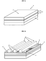
- Figure 1a is a simplified perspective view of a semiconductor laser or basic laser diode 10 comprising a semiconductor substrate 11 and an expitaxial structure 12 grown thereon.
- Part of the epitaxial structure 12 is formed by a laser layer 13 based on a buffer and contact layer 14 and covered at the top by a covering layer 15.
- the active region in the laser layer 13 can for example consist of a single quantum well or several quantum wells. It could also consist of a single layer of quantum dots or several stacked layers of quantum dots.
- the basic laser diode 10 shown in Figure 1a is of cuboid formation with a flat diode surface 16.
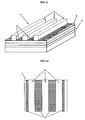
- the embodiment of an array of optically coupled ridge waveguide DFB laser diodes with a lateral grating structure 22 according to the invention shown in Figure 1c and 1d is produced in two essential process phases.
- Fig. 1a As a translational stage following the implementation of a first process phase, Fig.
- FIG. 1b shows a waveguide diode 17 in which the diode surface 16 has been subjected to a material removal process, such as for example a dry or wet etching process, in order to obtain the illustrated stepped surface formation with a number of waveguide ridges 18 aligned parallel to each other and extending in the longitudinal direction of the waveguide diode 17.
- the spacing between the waveguide ridges can be varied over the array, as it may be advantageous for the performance of the device to have the ridges at a non-equidistant spacing. Furthermore, it may be advantageous to use a different width for each of the waveguiding ridges in the array.
- the aforementioned material removal process gives rise to surfaces 19, which are formed between the waveguide ridges 18.
- flat surfaces 20 and 21 are created lateral to the outermost waveguides. These surfaces will be referred to in the following as carrier surfaces.
- the carrier surfaces are being covered by a thin insulating layer 26.
- the embodiment of an array of optically coupled ridge waveguide DFB laser diodes with a lateral grating structure 22 shown in figure 1c and 1d is produced by forming a metallic lattice structure 23 which is arranged on the carrier surface 19 by subjecting the carrier surface 19 to a lithographic process (e.g. by electron beam lithography) and a following metallization process not described in detail here.
- a metallic lattice structure can also be formed on the outer carrier surfaces 20 and 21, again by the application of a lithographic process.
- This second process phase results in an array of optically coupled ridge waveguide DFB laser diodes with lateral grating structures 22 illustrated in Figure 1c and 1d with the metallic lattice structure 23 arranged on the carrier surfaces 19, 20 and 21 above the laser layer 13.
- the insulating layer 26 can be utilized to define precisely the position of the structural regions 19, 20 and 21 of the metallic lattice structure 23 arranged on the epitaxial structure 12 relative to the laser layer 13.
- This insulating layer 26 can be provided in the form of an etch stop layer included in the expitaxial structure 12 which defines the depth of the lithographic structure produced using an etching process and thereby defines the position of the metallic lattice structure 23 relative to the laser layer 13.
- the insulating layer 26 can also be provided by an additionally deposited layer, which again defines the position of the metallic lattice relative to the laser layer 13.
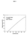
- FIG. 3 an illustration is given of how the maximum output power of an array of ridge waveguide lasers depends on the number of coupled ridge waveguide lasers. The deviation from a linear dependence of the output power on the pump current seen in the figure is caused by heating of the device.
- a single ridge waveguide shows a saturation of the ouput power at a current of 150 mA and an output power of 35 mW. If four waveguide ridges are coupled, saturation occurs at a much higher current and a power level of over 110 mW is reached.
- Figure 4 shows the output power characteristic of two coupled ridge waveguides with a lateral lattice. An output power of over 50 mW is obtained.
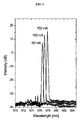
- Figure 5 shows the emission spectrum of the array with two coupled ridge waveguides and lateral lattice for three different drive currents. Monomode operation of the device is obtained for all currents. The shift of the laser emission to larger wavelength for increasing drive currents is due to heating, which changes the effective refractive index.
Landscapes
- Physics & Mathematics (AREA)
- Condensed Matter Physics & Semiconductors (AREA)
- General Physics & Mathematics (AREA)
- Electromagnetism (AREA)
- Optics & Photonics (AREA)
- Semiconductor Lasers (AREA)
Priority Applications (4)
| Application Number | Priority Date | Filing Date | Title |
|---|---|---|---|
| DE2002619884 DE60219884T2 (de) | 2002-03-08 | 2002-03-08 | Ein Halbleiterlaserarray mit seitlicher Gratingstruktur |
| EP02005165A EP1343232B1 (fr) | 2002-03-08 | 2002-03-08 | Barrette de lasers semiconducteurs à réseau latéral |
| AT02005165T ATE361565T1 (de) | 2002-03-08 | 2002-03-08 | Ein halbleiterlaserarray mit seitlicher gratingstruktur |
| US10/734,104 US7177335B2 (en) | 2002-03-08 | 2003-12-11 | Semiconductor laser array with a lattice structure |
Applications Claiming Priority (2)
| Application Number | Priority Date | Filing Date | Title |
|---|---|---|---|
| EP02005165A EP1343232B1 (fr) | 2002-03-08 | 2002-03-08 | Barrette de lasers semiconducteurs à réseau latéral |
| US10/734,104 US7177335B2 (en) | 2002-03-08 | 2003-12-11 | Semiconductor laser array with a lattice structure |
Publications (2)
| Publication Number | Publication Date |
|---|---|
| EP1343232A1 true EP1343232A1 (fr) | 2003-09-10 |
| EP1343232B1 EP1343232B1 (fr) | 2007-05-02 |
Family
ID=34809715
Family Applications (1)
| Application Number | Title | Priority Date | Filing Date |
|---|---|---|---|
| EP02005165A Expired - Lifetime EP1343232B1 (fr) | 2002-03-08 | 2002-03-08 | Barrette de lasers semiconducteurs à réseau latéral |
Country Status (3)
| Country | Link |
|---|---|
| US (1) | US7177335B2 (fr) |
| EP (1) | EP1343232B1 (fr) |
| AT (1) | ATE361565T1 (fr) |
Cited By (4)
| Publication number | Priority date | Publication date | Assignee | Title |
|---|---|---|---|---|
| WO2006082408A2 (fr) * | 2005-02-02 | 2006-08-10 | The Centre For Integrated Photonics Limited | Source laser |
| WO2008031197A1 (fr) * | 2006-09-12 | 2008-03-20 | Onechip Photonics Inc. | Dispositif à couplage amélioré comprenant une réseau gravé sur la surface et des arêtes latérales effectives |
| US7772022B2 (en) | 2005-06-03 | 2010-08-10 | The Centre For Integrated Photonics Limited | Method of aligning optical components with waveguides |
| CN104201566A (zh) * | 2014-08-22 | 2014-12-10 | 华中科技大学 | 一种具有高单纵模成品率的脊波导分布反馈半导体激光器 |
Families Citing this family (16)
| Publication number | Priority date | Publication date | Assignee | Title |
|---|---|---|---|---|
| EP1283571B1 (fr) * | 2001-08-06 | 2015-01-14 | nanoplus GmbH Nanosystems and Technologies | Laser avec réseau à couplage faible |
| US7477670B2 (en) * | 2004-05-27 | 2009-01-13 | Sarnoff Corporation | High power diode laser based source |
| JP4721924B2 (ja) * | 2005-12-09 | 2011-07-13 | 富士通株式会社 | 光導波路を伝搬する光と回折格子とを結合させた光素子 |
| JP4881056B2 (ja) * | 2006-05-01 | 2012-02-22 | キヤノン株式会社 | 電磁波吸収体部を含むフォトニック結晶電磁波デバイス、及びその製造方法 |
| JP4817255B2 (ja) * | 2006-12-14 | 2011-11-16 | 富士通株式会社 | 光半導体素子及びその製造方法 |
| KR100839343B1 (ko) * | 2007-01-23 | 2008-06-17 | 광주과학기술원 | 반도체 레이저 소자 및 그 제조 방법 |
| JP4312239B2 (ja) | 2007-02-16 | 2009-08-12 | 富士通株式会社 | 光素子及びその製造方法 |
| US7623560B2 (en) * | 2007-09-27 | 2009-11-24 | Ostendo Technologies, Inc. | Quantum photonic imagers and methods of fabrication thereof |
| US9455551B2 (en) * | 2012-01-13 | 2016-09-27 | Thorlabs Quantum Electronics, Inc. | Mid-IR multiwavelength concatenated distributed-feedback laser with an active core made of cascaded stages |
| CN102611002B (zh) * | 2012-03-23 | 2013-11-27 | 中国科学院长春光学精密机械与物理研究所 | 低发散角全布拉格反射波导半导体激光器阵列 |
| CN104184045B (zh) * | 2014-08-22 | 2017-04-05 | 华中科技大学 | 一种定波长单纵模工作的脊波导分布反馈半导体激光器 |
| CN105914580B (zh) * | 2016-07-07 | 2019-01-29 | 北京工业大学 | 具有侧向光栅和纵向布喇格反射镜结构的半导体激光器 |
| WO2018043229A1 (fr) * | 2016-08-30 | 2018-03-08 | パナソニックIpマネジメント株式会社 | Élément laser à semi-conducteurs |
| CN109462144A (zh) * | 2018-11-09 | 2019-03-12 | 中国工程物理研究院电子工程研究所 | 一种GaN基低阶表面光栅DFB激光器的制备方法 |
| EP3832817A1 (fr) * | 2019-12-03 | 2021-06-09 | nanoplus Nanosystems and Technologies GmbH | Laser semi-conducteur ainsi que procédé de fabrication d'un laser semi-conducteur |
| CN113948968B (zh) * | 2020-07-16 | 2023-10-03 | 山东华光光电子股份有限公司 | 一种实现基侧模激射的半导体激光器及其制备方法 |
Citations (3)
| Publication number | Priority date | Publication date | Assignee | Title |
|---|---|---|---|---|
| EP0363076A2 (fr) * | 1988-10-07 | 1990-04-11 | Trw Inc. | Réseau à laser à semi-conducteur à haute puissance et à faisceau de haute qualité |
| EP0786843A1 (fr) * | 1996-01-29 | 1997-07-30 | France Telecom | Composant d'émission laser multilongueur d'onde |
| EP1139527A2 (fr) * | 2000-03-27 | 2001-10-04 | Matsushita Electric Industrial Co., Ltd. | Dispositif réseau laser à semiconducteur à haute puissance |
Family Cites Families (17)
| Publication number | Priority date | Publication date | Assignee | Title |
|---|---|---|---|---|
| GB8406432D0 (en) * | 1984-03-12 | 1984-04-18 | British Telecomm | Semiconductor devices |
| GB8522308D0 (en) * | 1985-09-09 | 1985-10-16 | British Telecomm | Semiconductor lasers |
| US5422904A (en) * | 1991-12-31 | 1995-06-06 | Biota Corp. | Method of and means for controlling the electromagnetic output power of electro-optic semiconductor devices |
| US5345459A (en) * | 1993-09-09 | 1994-09-06 | Northern Telecom Limited | Method of reducing the thermally-induced shift in the emission wavelength of laser diodes |
| US5509025A (en) | 1994-04-04 | 1996-04-16 | At&T Corp. | Unipolar semiconductor laser |
| US5457709A (en) | 1994-04-04 | 1995-10-10 | At&T Ipm Corp. | Unipolar semiconductor laser |
| US5936989A (en) | 1997-04-29 | 1999-08-10 | Lucent Technologies, Inc. | Quantum cascade laser |
| US5978397A (en) | 1997-03-27 | 1999-11-02 | Lucent Technologies Inc. | Article comprising an electric field-tunable semiconductor laser |
| US5901168A (en) | 1997-05-07 | 1999-05-04 | Lucent Technologies Inc. | Article comprising an improved QC laser |
| US6137817A (en) | 1998-06-12 | 2000-10-24 | Lucent Technologies Inc. | Quantum cascade laser |
| DE29815522U1 (de) * | 1998-08-31 | 1998-12-03 | Forchel, Alfred, Prof. Dr., 97074 Würzburg | Halbleiterlaser mit Gitterstruktur |
| ES2247750T3 (es) * | 1998-08-31 | 2006-03-01 | Alfred Prof. Dr. Forchel | Laser de semiconductor con estructura de rejilla. |
| US6501783B1 (en) | 2000-02-24 | 2002-12-31 | Lucent Technologies Inc. | Distributed feedback surface plasmon laser |
| US6400744B1 (en) | 2000-02-25 | 2002-06-04 | Lucent Technologies, Inc. | Apparatus comprising a quantum cascade laser having improved distributed feedback for single-mode operation |
| EP1130724A1 (fr) | 2000-03-03 | 2001-09-05 | Alpes Lasers | Laser à cascade quantique et procédé pour la fabrication d'un tel laser |
| US6560259B1 (en) | 2000-05-31 | 2003-05-06 | Applied Optoelectronics, Inc. | Spatially coherent surface-emitting, grating coupled quantum cascade laser with unstable resonance cavity |
| EP1195865A1 (fr) | 2000-08-31 | 2002-04-10 | Alpes Lasers SA | Laser à cascades quantiques |
-
2002
- 2002-03-08 AT AT02005165T patent/ATE361565T1/de active
- 2002-03-08 EP EP02005165A patent/EP1343232B1/fr not_active Expired - Lifetime
-
2003
- 2003-12-11 US US10/734,104 patent/US7177335B2/en not_active Expired - Lifetime
Patent Citations (3)
| Publication number | Priority date | Publication date | Assignee | Title |
|---|---|---|---|---|
| EP0363076A2 (fr) * | 1988-10-07 | 1990-04-11 | Trw Inc. | Réseau à laser à semi-conducteur à haute puissance et à faisceau de haute qualité |
| EP0786843A1 (fr) * | 1996-01-29 | 1997-07-30 | France Telecom | Composant d'émission laser multilongueur d'onde |
| EP1139527A2 (fr) * | 2000-03-27 | 2001-10-04 | Matsushita Electric Industrial Co., Ltd. | Dispositif réseau laser à semiconducteur à haute puissance |
Non-Patent Citations (1)
| Title |
|---|
| KAMP M ET AL: "Lateral coupling - a material independent way to complex coupled DFB lasers", OPTICAL MATERIALS, ELSEVIER SCIENCE PUBLISHERS B.V. AMSTERDAM, NL, vol. 17, no. 1-2, June 2001 (2001-06-01), pages 19 - 25, XP004254783, ISSN: 0925-3467 * |
Cited By (8)
| Publication number | Priority date | Publication date | Assignee | Title |
|---|---|---|---|---|
| WO2006082408A2 (fr) * | 2005-02-02 | 2006-08-10 | The Centre For Integrated Photonics Limited | Source laser |
| WO2006082408A3 (fr) * | 2005-02-02 | 2006-10-19 | Ct Integrated Photonics Ltd | Source laser |
| US7715090B2 (en) | 2005-02-02 | 2010-05-11 | The Centre For Integrated Photonics Limited | Laser source |
| US7772022B2 (en) | 2005-06-03 | 2010-08-10 | The Centre For Integrated Photonics Limited | Method of aligning optical components with waveguides |
| WO2008031197A1 (fr) * | 2006-09-12 | 2008-03-20 | Onechip Photonics Inc. | Dispositif à couplage amélioré comprenant une réseau gravé sur la surface et des arêtes latérales effectives |
| US7609919B2 (en) | 2006-09-12 | 2009-10-27 | Onechip Photonics | Coupling-enhanced surface etched gratings |
| CN104201566A (zh) * | 2014-08-22 | 2014-12-10 | 华中科技大学 | 一种具有高单纵模成品率的脊波导分布反馈半导体激光器 |
| CN104201566B (zh) * | 2014-08-22 | 2017-12-29 | 华中科技大学 | 一种具有高单纵模成品率的脊波导分布反馈半导体激光器 |
Also Published As
| Publication number | Publication date |
|---|---|
| US7177335B2 (en) | 2007-02-13 |
| ATE361565T1 (de) | 2007-05-15 |
| EP1343232B1 (fr) | 2007-05-02 |
| US20050129084A1 (en) | 2005-06-16 |
Similar Documents
| Publication | Publication Date | Title |
|---|---|---|
| EP1343232B1 (fr) | Barrette de lasers semiconducteurs à réseau latéral | |
| JP2959902B2 (ja) | 半導体レーザとそれを有する装置とその製造方法 | |
| US7494836B2 (en) | Semiconductor laser with a weakly coupled grating | |
| US5208183A (en) | Method of making a semiconductor laser | |
| US7696098B2 (en) | Tuneable unipolar lasers | |
| CN102113187B (zh) | 带有相结构的边发射的半导体激光器 | |
| CN107565381B (zh) | 分布反馈式半导体激光器装置及光子集成发射芯片模块 | |
| JP3891223B2 (ja) | レーザーおよびそれに関連する改良 | |
| US7981707B2 (en) | Method for enhancing optical characteristics of multilayer optoelectronic components | |
| EP1012933B1 (fr) | Dispositif laser | |
| JPH03110884A (ja) | 分布帰還型半導体レーザーおよびその製造方法 | |
| JPH0724324B2 (ja) | 半導体レーザ・チップおよびその製造方法 | |
| JPH0697604A (ja) | 分布反射型半導体レーザ | |
| CN113812049A (zh) | 一种用于光子集成电路的分布式反馈激光器装置及其改进和制造方法 | |
| US6865207B1 (en) | Semiconductor laser device withspot-size converter and method for fabricating the same | |
| JP4992451B2 (ja) | 半導体レーザ、および半導体レーザを作製する方法 | |
| EP1304780B1 (fr) | Laser à semiconducteur accordable sur bande large | |
| JP4111279B2 (ja) | 波長制御を伴うファブリペローレーザ | |
| JPH0697578A (ja) | 半導体レーザアレイ | |
| JP2011258713A (ja) | 分布帰還型半導体レーザ素子の作製方法 | |
| JPH02263490A (ja) | 波長可変半導体レーザ | |
| Li | Optical mode switching with a coupled triple-stripe injection laser | |
| SHIMADA et al. | Tunable external-cavity quantum-well laser using grating coupler integrated in selectively disordered waveguide | |
| JPH0430490A (ja) | 半導体レーザ素子とその製造方法 | |
| JP2003324245A (ja) | 半導体レーザ |
Legal Events
| Date | Code | Title | Description |
|---|---|---|---|
| PUAI | Public reference made under article 153(3) epc to a published international application that has entered the european phase |
Free format text: ORIGINAL CODE: 0009012 |
|
| AK | Designated contracting states |
Kind code of ref document: A1 Designated state(s): AT BE CH CY DE DK ES FI FR GB GR IE IT LI LU MC NL PT SE TR |
|
| AX | Request for extension of the european patent |
Extension state: AL LT LV MK RO SI |
|
| 17P | Request for examination filed |
Effective date: 20040308 |
|
| AKX | Designation fees paid |
Designated state(s): AT BE CH CY DE DK ES FI FR GB GR IE IT LI LU MC NL PT SE TR |
|
| 17Q | First examination report despatched |
Effective date: 20040709 |
|
| GRAP | Despatch of communication of intention to grant a patent |
Free format text: ORIGINAL CODE: EPIDOSNIGR1 |
|
| GRAS | Grant fee paid |
Free format text: ORIGINAL CODE: EPIDOSNIGR3 |
|
| GRAA | (expected) grant |
Free format text: ORIGINAL CODE: 0009210 |
|
| RIN1 | Information on inventor provided before grant (corrected) |
Inventor name: KAMP, MARTIN Inventor name: MUELLER, MARTIN |
|
| AK | Designated contracting states |
Kind code of ref document: B1 Designated state(s): AT BE CH CY DE DK ES FI FR GB GR IE IT LI LU MC NL PT SE TR |
|
| PG25 | Lapsed in a contracting state [announced via postgrant information from national office to epo] |
Ref country code: FI Free format text: LAPSE BECAUSE OF FAILURE TO SUBMIT A TRANSLATION OF THE DESCRIPTION OR TO PAY THE FEE WITHIN THE PRESCRIBED TIME-LIMIT Effective date: 20070502 |
|
| REG | Reference to a national code |
Ref country code: GB Ref legal event code: FG4D |
|
| REG | Reference to a national code |
Ref country code: CH Ref legal event code: EP |
|
| REG | Reference to a national code |
Ref country code: IE Ref legal event code: FG4D |
|
| REF | Corresponds to: |
Ref document number: 60219884 Country of ref document: DE Date of ref document: 20070614 Kind code of ref document: P |
|
| PG25 | Lapsed in a contracting state [announced via postgrant information from national office to epo] |
Ref country code: ES Free format text: LAPSE BECAUSE OF FAILURE TO SUBMIT A TRANSLATION OF THE DESCRIPTION OR TO PAY THE FEE WITHIN THE PRESCRIBED TIME-LIMIT Effective date: 20070813 |
|
| REG | Reference to a national code |
Ref country code: CH Ref legal event code: NV Representative=s name: HEPP, WENGER & RYFFEL AG |
|
| REG | Reference to a national code |
Ref country code: SE Ref legal event code: TRGR |
|
| ET | Fr: translation filed | ||
| NLV1 | Nl: lapsed or annulled due to failure to fulfill the requirements of art. 29p and 29m of the patents act | ||
| PG25 | Lapsed in a contracting state [announced via postgrant information from national office to epo] |
Ref country code: NL Free format text: LAPSE BECAUSE OF FAILURE TO SUBMIT A TRANSLATION OF THE DESCRIPTION OR TO PAY THE FEE WITHIN THE PRESCRIBED TIME-LIMIT Effective date: 20070502 Ref country code: DK Free format text: LAPSE BECAUSE OF FAILURE TO SUBMIT A TRANSLATION OF THE DESCRIPTION OR TO PAY THE FEE WITHIN THE PRESCRIBED TIME-LIMIT Effective date: 20070502 Ref country code: PT Free format text: LAPSE BECAUSE OF FAILURE TO SUBMIT A TRANSLATION OF THE DESCRIPTION OR TO PAY THE FEE WITHIN THE PRESCRIBED TIME-LIMIT Effective date: 20071002 |
|
| PLBE | No opposition filed within time limit |
Free format text: ORIGINAL CODE: 0009261 |
|
| STAA | Information on the status of an ep patent application or granted ep patent |
Free format text: STATUS: NO OPPOSITION FILED WITHIN TIME LIMIT |
|
| 26N | No opposition filed |
Effective date: 20080205 |
|
| PG25 | Lapsed in a contracting state [announced via postgrant information from national office to epo] |
Ref country code: GR Free format text: LAPSE BECAUSE OF FAILURE TO SUBMIT A TRANSLATION OF THE DESCRIPTION OR TO PAY THE FEE WITHIN THE PRESCRIBED TIME-LIMIT Effective date: 20070803 |
|
| PG25 | Lapsed in a contracting state [announced via postgrant information from national office to epo] |
Ref country code: MC Free format text: LAPSE BECAUSE OF NON-PAYMENT OF DUE FEES Effective date: 20080331 |
|
| PG25 | Lapsed in a contracting state [announced via postgrant information from national office to epo] |
Ref country code: CY Free format text: LAPSE BECAUSE OF FAILURE TO SUBMIT A TRANSLATION OF THE DESCRIPTION OR TO PAY THE FEE WITHIN THE PRESCRIBED TIME-LIMIT Effective date: 20070502 |
|
| PG25 | Lapsed in a contracting state [announced via postgrant information from national office to epo] |
Ref country code: LU Free format text: LAPSE BECAUSE OF NON-PAYMENT OF DUE FEES Effective date: 20080308 |
|
| PG25 | Lapsed in a contracting state [announced via postgrant information from national office to epo] |
Ref country code: TR Free format text: LAPSE BECAUSE OF FAILURE TO SUBMIT A TRANSLATION OF THE DESCRIPTION OR TO PAY THE FEE WITHIN THE PRESCRIBED TIME-LIMIT Effective date: 20070502 |
|
| REG | Reference to a national code |
Ref country code: FR Ref legal event code: PLFP Year of fee payment: 15 |
|
| REG | Reference to a national code |
Ref country code: FR Ref legal event code: PLFP Year of fee payment: 16 |
|
| REG | Reference to a national code |
Ref country code: FR Ref legal event code: PLFP Year of fee payment: 17 |
|
| PGFP | Annual fee paid to national office [announced via postgrant information from national office to epo] |
Ref country code: IE Payment date: 20200218 Year of fee payment: 19 |
|
| PGFP | Annual fee paid to national office [announced via postgrant information from national office to epo] |
Ref country code: FR Payment date: 20210310 Year of fee payment: 20 |
|
| PGFP | Annual fee paid to national office [announced via postgrant information from national office to epo] |
Ref country code: GB Payment date: 20210317 Year of fee payment: 20 |
|
| PGFP | Annual fee paid to national office [announced via postgrant information from national office to epo] |
Ref country code: DE Payment date: 20210615 Year of fee payment: 20 Ref country code: IT Payment date: 20210430 Year of fee payment: 20 |
|
| PGFP | Annual fee paid to national office [announced via postgrant information from national office to epo] |
Ref country code: SE Payment date: 20210416 Year of fee payment: 20 Ref country code: AT Payment date: 20210615 Year of fee payment: 20 Ref country code: BE Payment date: 20210615 Year of fee payment: 20 Ref country code: CH Payment date: 20210617 Year of fee payment: 20 |
|
| PG25 | Lapsed in a contracting state [announced via postgrant information from national office to epo] |
Ref country code: IE Free format text: LAPSE BECAUSE OF NON-PAYMENT OF DUE FEES Effective date: 20210308 |
|
| REG | Reference to a national code |
Ref country code: DE Ref legal event code: R071 Ref document number: 60219884 Country of ref document: DE |
|
| REG | Reference to a national code |
Ref country code: CH Ref legal event code: PL |
|
| REG | Reference to a national code |
Ref country code: GB Ref legal event code: PE20 Expiry date: 20220307 |
|
| REG | Reference to a national code |
Ref country code: BE Ref legal event code: MK Effective date: 20220308 |
|
| REG | Reference to a national code |
Ref country code: AT Ref legal event code: MK07 Ref document number: 361565 Country of ref document: AT Kind code of ref document: T Effective date: 20220308 |
|
| PG25 | Lapsed in a contracting state [announced via postgrant information from national office to epo] |
Ref country code: GB Free format text: LAPSE BECAUSE OF EXPIRATION OF PROTECTION Effective date: 20220307 |
|
| REG | Reference to a national code |
Ref country code: SE Ref legal event code: EUG |