EP1341118B1 - Appareil opto-électronique - Google Patents
Appareil opto-électronique Download PDFInfo
- Publication number
- EP1341118B1 EP1341118B1 EP03003883A EP03003883A EP1341118B1 EP 1341118 B1 EP1341118 B1 EP 1341118B1 EP 03003883 A EP03003883 A EP 03003883A EP 03003883 A EP03003883 A EP 03003883A EP 1341118 B1 EP1341118 B1 EP 1341118B1
- Authority
- EP
- European Patent Office
- Prior art keywords
- receiver
- optoelectronic device
- light beams
- insert
- transmitted light
- Prior art date
- Legal status (The legal status is an assumption and is not a legal conclusion. Google has not performed a legal analysis and makes no representation as to the accuracy of the status listed.)
- Expired - Lifetime
Links
- 230000005693 optoelectronics Effects 0.000 title claims description 48
- 230000003287 optical effect Effects 0.000 claims description 12
- 238000012544 monitoring process Methods 0.000 claims description 8
- 238000001514 detection method Methods 0.000 claims description 5
- 238000011156 evaluation Methods 0.000 claims description 5
- 239000004020 conductor Substances 0.000 claims description 3
- 229920003023 plastic Polymers 0.000 claims description 2
- 239000004033 plastic Substances 0.000 claims description 2
- 239000000463 material Substances 0.000 claims 1
- 239000002184 metal Substances 0.000 claims 1
- 238000000926 separation method Methods 0.000 description 4
- 230000005855 radiation Effects 0.000 description 2
- 229910001229 Pot metal Inorganic materials 0.000 description 1
- 108010076504 Protein Sorting Signals Proteins 0.000 description 1
- 241000287219 Serinus canaria Species 0.000 description 1
- HCHKCACWOHOZIP-UHFFFAOYSA-N Zinc Chemical group [Zn] HCHKCACWOHOZIP-UHFFFAOYSA-N 0.000 description 1
- 230000005540 biological transmission Effects 0.000 description 1
- 238000010276 construction Methods 0.000 description 1
- 238000011161 development Methods 0.000 description 1
- 230000018109 developmental process Effects 0.000 description 1
- 230000001771 impaired effect Effects 0.000 description 1
- 238000002347 injection Methods 0.000 description 1
- 239000007924 injection Substances 0.000 description 1
- 230000002452 interceptive effect Effects 0.000 description 1
- 238000004519 manufacturing process Methods 0.000 description 1
- 230000035945 sensitivity Effects 0.000 description 1
- 230000001629 suppression Effects 0.000 description 1
- 238000011144 upstream manufacturing Methods 0.000 description 1
Images


Classifications
-
- G—PHYSICS
- G06—COMPUTING; CALCULATING OR COUNTING
- G06K—GRAPHICAL DATA READING; PRESENTATION OF DATA; RECORD CARRIERS; HANDLING RECORD CARRIERS
- G06K7/00—Methods or arrangements for sensing record carriers, e.g. for reading patterns
- G06K7/10—Methods or arrangements for sensing record carriers, e.g. for reading patterns by electromagnetic radiation, e.g. optical sensing; by corpuscular radiation
- G06K7/10544—Methods or arrangements for sensing record carriers, e.g. for reading patterns by electromagnetic radiation, e.g. optical sensing; by corpuscular radiation by scanning of the records by radiation in the optical part of the electromagnetic spectrum
- G06K7/10792—Special measures in relation to the object to be scanned
-
- G—PHYSICS
- G06—COMPUTING; CALCULATING OR COUNTING
- G06K—GRAPHICAL DATA READING; PRESENTATION OF DATA; RECORD CARRIERS; HANDLING RECORD CARRIERS
- G06K7/00—Methods or arrangements for sensing record carriers, e.g. for reading patterns
- G06K7/10—Methods or arrangements for sensing record carriers, e.g. for reading patterns by electromagnetic radiation, e.g. optical sensing; by corpuscular radiation
- G06K7/10544—Methods or arrangements for sensing record carriers, e.g. for reading patterns by electromagnetic radiation, e.g. optical sensing; by corpuscular radiation by scanning of the records by radiation in the optical part of the electromagnetic spectrum
- G06K7/10554—Moving beam scanning
- G06K7/10594—Beam path
- G06K7/10683—Arrangement of fixed elements
- G06K7/10702—Particularities of propagating elements, e.g. lenses, mirrors
Definitions
- the invention relates to an optoelectronic device according to the preamble of claim 1.
- Such an optoelectronic device is known from DE 198 44 238 A1. This optoelectronic device is used to detect brands, which are designed in particular as barcodes.
- the optoelectronic device has a transmitter with a downstream transmitting optics and a receiver with an upstream receiving optics.
- the transmitted light beams emitted by the transmitter and the received light beams reflected by the marks are passed through a deflection unit.
- the deflection unit consists of a rotating polygon mirror wheel with a predetermined number of mirror surfaces. By means of the deflection unit, the transmitted light beams are periodically guided within a monitoring area.
- various deflecting mirrors are arranged between the transmitter and the deflecting unit on the one hand and between the receiver and the deflecting unit, via which the transmitted light beams and received light beams are guided.
- the optoelectronic device thus has a multiplicity of optical components, via which the transmitted light beams and received light beams must be guided.
- the individual components in particular the deflecting mirror, must be adjusted in a suitable manner. This creates an undesirably high assembly costs in the manufacture of the optoelectronic device.
- the optoelectronic device has an undesirably large design, since in particular the arrangement of the deflecting mirrors and the receiving optics in front of the receiver requires a large amount of space.
- a further generic optoelectronic device for detecting barcodes is known.
- the transmitter and the receiver are arranged one above the other at a distance from each other.
- the transmitted light rays emitted by the transmitter and the received light beams reflected back from the marks are passed through a deflection unit.
- the deflection unit is formed by a polygon mirror wheel having a predetermined number of mirror surfaces.
- the transmitted light beams and received light beams are respectively guided over the same mirror surface of the polygon mirror wheel.
- the transmitted light beams and received light beams are guided spatially separated from each other, so that the transmitted light beams strike the upper sub-segment of the respective mirror surface of the polygon mirror wheel, while the received light beams are guided over the lower sub-segment of the same mirror surface.
- the sub-segments of the mirror surface to which the Transmitted light beams and received light beams meet clearly offset from each other.
- the height of the polygon mirror wheel compared to conventional polygon mirror wheels must be significantly increased in order to obtain the desired separation of the transmitted and received light beams. This in turn requires an undesirable increase in the design of the optoelectronic device.
- the invention has for its object an optoelectronic device of the type mentioned in such a way that it has the highest possible detection reliability with the smallest possible design.
- the optoelectronic device is used to detect marks provided with contrast patterns and has a transmitting light beam emitting transmitter, a receiving light beam receiving receiver, a deflection unit, by means of which the transmitted light beams are guided periodically within a monitoring area, and an evaluation unit for evaluating the pending at the output of the receiver receive signals on.
- the receiver is mounted in an opaque insert which has channel structures extending in the direction of the optical axis of the receiver, in which the received light beams reflected by the deflection unit are guided to the receiver.
- An essential advantage of the invention is that the receiver mounted in the insert is opposite the deflecting unit without the interposition of a receiving optical unit and deflecting mirrors.
- the distance between the receiver and deflector can thus be kept very low, whereby the size the optoelectronic device is reduced accordingly.
- this significantly reduces the number of optical components of the optoelectronic device, as a result of which it is simple and inexpensive to produce.
- Another important advantage of the optoelectronic device according to the invention is that the interference and external light irradiation to the receiver is substantially reduced by the guidance of the received light beams in the channel structures of the insert, whereby a high detection reliability of the optoelectronic device is obtained.
- the geometry of the insert is optimally adapted to the beam guidance of the received light beams in that the channels of the channel structures are parallel to the optical axis of the receiver.
- the receiving light beams running along the optical axis thus strike the receiver almost unhindered.
- obliquely incident interfering and extraneous light radiations strike the opaque wall elements of the channel structures, so that they no longer strike the receiver.
- the channel structures are as long as possible and reach close to the deflection unit.
- the channel structures have a honeycomb structure with a plurality of channels whose diameters are considerably smaller than their lengths. This ensures that incident and extraneous light rays impinge on the wall elements of the channel structures and not on the receiver even at low angles to the optical axis of the receiver.
- the wall elements of the channel structures are roughened or structured and thus act as light traps for the interference and extraneous light beams, that is to say they are prevented from reaching the receiver as a result of multiple reflections on the wall elements.
- the insert may consist of conductive material, so that with this also an EMC (Electromagnetic Compatibility) protection of the receiver is obtained.
- EMC Electromagnetic Compatibility
- the transmitted light beams and received light beams extend coaxially.
- the transmitter is also arranged in use and is located directly behind the receiver.
- the transmitted light beams are guided through a recess in the photosensitive surface of the receiver, whereby the transmitted light beams are at least partially enclosed by the photosensitive surface.
- the transmitted light beams and received light beams are guided in this case in separate channels of the channel structure of the insert, whereby a nearly complete separation of the transmitted light beams and received light beams is obtained.
- this embodiment has a particularly compact construction.
- FIG. 1 schematically shows the structure of an optoelectronic device 1 for detecting marks provided with defined contrast patterns.
- the marks can have any desired sequences and shapes of adjoining light-dark areas, preferably black-and-white areas.
- the invention will be explained for the case where the marks of bar codes 2 are formed.
- the barcodes 2 essentially consist of a sequence of black and white line elements of defined length and width.
- the optoelectronic device 1 has a transmitting light rays 3 emitting transmitter 4 and a receiving light beams 5 receiving receiver 6.
- the transmitter 4 which is preferably formed by a laser diode, a transmitting optics 7 for focusing the transmitted light beams 3 is arranged downstream.
- the emitted light beams 3 emitted by the transmitter 4 and the received light beams 5 reflected back from the bar code 2 are guided via a deflection unit.
- the deflection unit consists of a motor-driven polygon mirror wheel 8 with a predetermined number of facet-shaped mirror surfaces 9.
- the transmitted light beams 3 are periodically guided in a monitoring area 10 which extends in a scanning plane.
- the monitoring area 10 extends over a certain angular range, which is predetermined by the number of mirror surfaces 9 of the polygon mirror wheel 8.
- the pending at the output of the receiver 6 received signals are amplified in an amplifier, not shown, and evaluated in an evaluation unit, also not shown.
- the received light beams 5, which are reflected at the bar codes 2, have an amplitude modulation corresponding to the sequence of black and white bar elements of the bar code 2.
- the pending at the output of the receiver 6 Receive signals have a corresponding amplitude modulation.
- the analog, amplitude-modulated received signals are evaluated in the evaluation unit by means of a threshold value unit. This results in binary signal sequences, on the basis of which, by comparison with stored contrast patterns of barcodes 2, the recognition of the barcode 2 takes place.
- the emitted light beams 3 emitted by the transmitter 4, which are guided onto the deflection unit and the received light beams 5 reflected back from the marks via the deflection unit to the receiver 6, run coaxially in the embodiment according to FIG.
- This coaxial beam guidance is achieved in that the photosensitive surface 11 of the receiver 6, which is arranged directly downstream of the transmitter 4 and the transmitting optics 7, at least partially surrounds the transmitted light beams 3.
- This beam guidance is achieved in that the receiver 6 and its photosensitive surface 11 have a recess 12 through which the transmitted light beams 3 are guided.
- the transmitter 4 and the receiver 6 are spaced apart from the polygon mirror wheel 8 such that the transmitted light beams 3 and the received light beams 5 are guided over the same mirror surface 9 of the polygon mirror wheel 8.
- the mirror surfaces 9 of the polygon mirror 8 are oriented in the present case perpendicular to the beam axes of the transmitted light beams 3 and 5 receive light beams.
- the received light spot imaged on a mirror surface 9 at least partially surrounds the transmitted light spot of the transmitted light beams 3 imaged on the same mirror surface 9.
- the mirror surfaces 9 are adapted to the geometries of the transmitted light beams 3 and received light beams 5 such that they illuminate the mirror surface 9 as completely as possible.
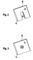
- FIGS 2 and 3 show two embodiments of the receiver 6 of the optoelectronic device 1 according to Figure 1.
- the receiver 6 has a large area, flat photosensitive surface 11 which has a substantially square outer contour.
- the photosensitive surface 11 is homogeneous in the embodiments according to Figures 2 and 3, that is integrally formed.
- the receiver 6 may consist of a number of receiving elements, which each have light-sensitive partial areas, which together form the photosensitive area 11.
- the receiver 6 is mounted on a support 13 which can be connected via connections, not shown, to a circuit board on which the evaluation unit is integrated.
- the cross-sectional area of the carrier 13 is adapted to the size of the photosensitive surface 11.
- the recess 12 extends from the center of the receiver 6 to its lower edge and terminates there.
- the recess 12 is formed by a circular, central bore, which passes through the photosensitive surface 11 and the carrier 13 located behind it.
- the diameter of the recesses are larger than the diameter of the transmitted light beams 3, so that they pass through the recess unhindered.
- the transmitter 4, the transmitting optics 7 and the receiver 6 with the carrier 13 form a structural unit, which are integrated in an opaque insert 14.
- the insert 14 is preferably made of a die-cast zinc part and thus of conductive material, so that this EMC protection for the stored in the interior of electrical or optoelectronic Components forms.
- the insert may be formed by a plastic injection molded part.
- the insert 14 has channel structures, in which the received light beams 5 and the transmitted light beams 3 are guided.
- the channel structures consist of a predetermined number of channels 15a, b, which are bounded by opaque wall elements 16 of the insert 14.
- the channel structures form a honeycomb structure, wherein the channels 15a, b each have a constant cross section.
- the longitudinal axes of the channels 15a, b extend parallel to the optical axes of the transmitter 4 and the receiver 6.
- the channels 15a, b delimiting wall elements 16 of the insert 14 close in front of the photosensitive surface 11 of the receiver 6, which are perpendicular to the longitudinal axes the channels 15a, b are oriented.
- the lengths of the channels 15a, b are dimensioned such that the channel structures are guided as close as possible to the deflection unit, without the scanning of the monitoring area 10 being hindered in this case. Therefore, as shown in Figure 1, the channels 15a, b in the region of the front edge of the polygon mirror 8 shorter than the channels 15a, b in the region of the center of the polygon mirror 8. This ensures that at maximum extent of the channel structures in the direction of the deflection Wall elements 16 of the insert 14 are outside the range of the monitoring area 10, which is swept by the received light beams 5 and transmitted light beams 3.
- the insert 14 significantly increases the detection sensitivity of the optoelectronic device 1. This is due to the fact that through the canary structures the received light beams 5 are almost completely guided by the deflection unit to the receiver 6, but interference and extraneous light radiations are blocked by the insert 14 so that they do not reach the receiver 6.
- the beam axes of the received light beams 5 reflected by the deflection unit run perpendicular to the plane of the photosensitive surface 11, while the interference and external light irradiation from a large angular range in the direction of the receiver 6 is utilized.
- the parallel to the beam axis of the received light beams 5 extending channels 15a, b, the receiving light beams 5 are guided without appreciable reflections on the wall elements 16 of the channel structures to the receiver 6. Since the cross section of the insert 14 is adapted to the size of the photosensitive surface 11, the received light beams 5 are almost completely guided onto the photosensitive surface 11 of the receiver 6.
- the predominantly incident at oblique angles to the channel structures interference and extraneous light rays hit the wall elements 16 of the channel structures and not on the receiver 6. Since the lengths of the channels 15a, b are chosen as large as possible, the interference and extraneous light beams would only after multiple Reflections on the wall elements 16 impinge on the receiver 6.
- the surfaces of the wall elements 16 are strongly light-absorbing. In addition, the surfaces are preferably roughened or structured. Thus, the wall elements 16 act as light traps, so that multiple reflections of interference and extraneous light beams are effectively prevented.
- the honeycomb channel structures have a predetermined number of elongate channels 15a, b with small cross-sectional areas relative to their lengths. This ensures that only such disturbance and Extraneous light rays reach the receiver 6, which extend along the optical axis of the receiver 6 or at a narrow angle thereto.
- FIGS. 4-6 Examples of such channel structures are shown in FIGS. 4-6.
- a plan view of the top side of the insert 14 is shown in FIGS. 4-6.
- the honeycomb structure of the insert 14 according to FIG. 4 corresponds to the insert 14 used in the optoelectronic device 1 according to FIG. 1, in which the transmitter 4 and the receiver 6 are arranged one behind the other.
- a receiver 6 is mounted in the insert 14 according to Figure 4, the photosensitive surface 11 has the shape shown in Figure 2.
- the channel structure of the insert 14 according to Figure 4 has two identically formed, mirror-symmetrically arranged channels 15a, in which the receiving light beams 5 are guided.
- the photosensitive surface 11 of the receiver 6 in the bottom region of the insert 14 is adapted to the geometries of the channels 15a so that it extends over the entire cross-sectional areas of the channels 15a.
- the channel structure of the insert 14 a channel 15 b, which opens at a side wall of the insert 14.
- this channel 15b emitted by the transmitter 4 transmitted light beams 3 are guided.
- the wall element 16 between this channel 15b and the two adjacent channels 15a an optical separation of the transmitted light beams 3 and the received light beams 5 is achieved.
- the beam cross section of the transmitted light beams 3 is smaller than the cross section of the channel 15a, so that in this case the transmitted light beams 3 are guided on the adjacent wall element 16 without reflections.
- FIG. 5 shows a further embodiment of an insert 14 which can be used for the optoelectronic device 1 according to FIG.
- the transmitter 4 and the receiver 6 are in turn arranged one behind the other in the bottom region of the receiver 6.
- the receiver 6 has the shape shown in Figure 3, that is, the transmitted light beams 3 are guided through a central bore in the photosensitive surface 11.
- the geometry of the channel structures of the insert 14 according to FIG. 5 is adapted to this transmitter-receiver structure.
- the insert 14 has four identically formed first channels 15a, in which the receiving light beams 5 extend and are guided to the photosensitive surface 11 of the receiver 6. Furthermore, a second channel 15b is provided with a circular cross section, in which the transmitted light beams 3 extend. The cross-sectional area of this channel 15b is larger than the beam cross section of the transmitted light beams 3 analogously to the exemplary embodiment according to FIG.
- FIG. 6 shows an embodiment of an insert 14 in which a receiver 6 can be introduced whose photosensitive surface 11 extends over the entire cross-sectional area of the interior of the insert 14.
- This insert 14 is suitable for an optoelectronic device 1, in which only the receiver 6 is arranged in the insert 14, whereas the transmitter 4 is located outside the insert 14.
- the insert 14 only channels 15a, in which the receiving light beams 5 are guided.
- the channels 15a are formed identically.
- channels 15a with different cross-sectional geometries can also be provided.
Landscapes
- Physics & Mathematics (AREA)
- Engineering & Computer Science (AREA)
- Electromagnetism (AREA)
- Artificial Intelligence (AREA)
- Toxicology (AREA)
- General Health & Medical Sciences (AREA)
- Health & Medical Sciences (AREA)
- Computer Vision & Pattern Recognition (AREA)
- General Physics & Mathematics (AREA)
- Theoretical Computer Science (AREA)
- Photo Coupler, Interrupter, Optical-To-Optical Conversion Devices (AREA)
- Mechanical Optical Scanning Systems (AREA)
- Geophysics And Detection Of Objects (AREA)
- Optical Communication System (AREA)
Claims (17)
- Dispositif optoélectronique pour la saisie de marques munies de motifs contrastés avec un émetteur émettant des rayons lumineux d'émission, un récepteur recevant des rayons lumineux de réception, une unité de déviation au moyen de laquelle les rayons lumineux d'émission sont périodiquement guidés à l'intérieur d'une zone de surveillance et une unité d'évaluation pour évaluer les signaux de réception disponibles à la sortie du récepteur, caractérisé par le fait que le récepteur (6) est monté dans un insert (14) opaque qui présente des structures en canal s'étendant dans la direction de l'axe optique du récepteur (6), dans lesquelles les rayons lumineux de réception (5) réfléchis par l'unité de déviation sont guidés vers le récepteur (6).
- Dispositif optoélectronique selon la revendication 1, caractérisé par le fait que le récepteur (6) est disposé dans le fond de l'insert (14) et que les structures en canal présentent des canaux (15a, b) qui sont limités par des éléments de paroi faisant saillie perpendiculairement du fond de l'insert (14).
- Dispositif optoélectronique selon la revendication 2, caractérisé par le fait que les structures en canal forment une structure en nid d'abeilles dont les canaux (15a, b) s'étendent perpendiculairement à l'axe optique du récepteur (6).
- Dispositif optoélectronique selon l'une des revendications 2 ou 3, caractérisé par le fait que la surface de section de l'insert (14) est adaptée à la grandeur de la surface photosensible (11) du récepteur (6).
- Dispositif optoélectronique selon la revendication 4, caractérisé par le fait que le récepteur (6) présente une surface photosensible (11) homogène et continue.
- Dispositif optoélectronique selon la revendication 4, caractérisé par le fait que le récepteur (6) est composé d'un nombre prédéfini d'éléments récepteurs dont les sous-surfaces photosensibles sont les constituants de la surface photosensible (11).
- Dispositif optoélectronique selon l'une des revendications 2 à 6, caractérisé par le fait que les éléments de paroi (16) de la structure en canal présente des surfaces rugueuses ou structurées.
- Dispositif optoélectronique selon l'une des revendications 1 à 7, caractérisé par le fait que l'insert (14) est constitué d'une pièce en métal moulé sous pression ou en matière plastique moulée par injection.
- Dispositif optoélectronique selon l'une des revendications 1 à 8, caractérisé par le fait que l'insert (14) est constitué d'un matériau électroconducteur.
- Dispositif optoélectronique selon l'une des revendications 1 à 9, caractérisé par le fait que l'émetteur (4) et le récepteur (6) sont disposés dans l'insert (14).
- Dispositif optoélectronique selon la revendication 10, caractérisé par le fait que les rayons lumineux d'émission (3) et les rayons lumineux de réception (5) sont guidés selon des trajectoires coaxiales au moyen de l'unité de déviation.
- Dispositif optoélectronique selon la revendication 11, caractérisé par le fait que la surface photosensible (11) du récepteur (6) entoure au moins partiellement les rayons lumineux d'émission (3).
- Dispositif optoélectronique selon l'une des revendications 11 ou 12, caractérisé par le fait que la surface photosensible (11) du récepteur (6) présente un évidement et que l'émetteur (4) est disposé derrière le récepteur (6) de telle manière que les rayons lumineux d'émission (3) sont guidés à travers l'évidement.
- Dispositif optoélectronique selon la revendication 13, caractérisé par le fait que l'évidement est réalisé sous la forme d'un trou central dans la surface photosensible (11) du récepteur (6).
- Dispositif optoélectronique selon la revendication 14, caractérisé par le fait que l'évidement débouche sur un bord du récepteur (6).
- Dispositif optoélectronique selon l'une des revendications 10 à 15, caractérisé par le fait que les rayons lumineux d'émission (3) et les rayons lumineux de réception (5) sont guidés dans des canaux séparés (15a, b) des structures en canal de l'insert (14).
- Dispositif optoélectronique selon l'une des revendications 1 à 16, caractérisé par le fait que l'unité de déviation est formée d'une roue à miroir polygonal (8) présentant un nombre prédéfini de faces réfléchissantes (9), le spot de lumière de réception des rayons lumineux de réception (5) représenté sur une face réfléchissante (9) entourant au moins partiellement le spot de lumière d'émission représenté sur la même face réfléchissante (9).
Applications Claiming Priority (2)
| Application Number | Priority Date | Filing Date | Title |
|---|---|---|---|
| DE10209269A DE10209269C1 (de) | 2002-03-01 | 2002-03-01 | Optoelektronische Vorrichtung |
| DE10209269 | 2002-03-01 |
Publications (2)
| Publication Number | Publication Date |
|---|---|
| EP1341118A1 EP1341118A1 (fr) | 2003-09-03 |
| EP1341118B1 true EP1341118B1 (fr) | 2006-09-06 |
Family
ID=7713996
Family Applications (1)
| Application Number | Title | Priority Date | Filing Date |
|---|---|---|---|
| EP03003883A Expired - Lifetime EP1341118B1 (fr) | 2002-03-01 | 2003-02-21 | Appareil opto-électronique |
Country Status (4)
| Country | Link |
|---|---|
| US (1) | US6817526B2 (fr) |
| EP (1) | EP1341118B1 (fr) |
| JP (1) | JP4375977B2 (fr) |
| DE (2) | DE10209269C1 (fr) |
Families Citing this family (1)
| Publication number | Priority date | Publication date | Assignee | Title |
|---|---|---|---|---|
| DE102008053881A1 (de) * | 2008-10-30 | 2010-05-12 | I.L.E.E. Ag Industrial Laser And Electronic Engineering | Reflexionsschranke mit Vermessungs- und / oder Lokalisierungsfunktion |
Family Cites Families (9)
| Publication number | Priority date | Publication date | Assignee | Title |
|---|---|---|---|---|
| US4916318A (en) * | 1986-12-16 | 1990-04-10 | Asahi Kogaku Kogyo K.K. | Scan type optical reader with changing beam waist position |
| EP0572685B1 (fr) * | 1992-05-18 | 1998-08-12 | Sumitomo Electric Industries, Ltd. | Dispositif de lecture de symboles avec variation du foyer d'un rayon de balayage laser par modification de la longueur de son chemin optique |
| ATE250782T1 (de) * | 1996-01-27 | 2003-10-15 | Datalogic Spa | Abtaster |
| US6075883A (en) * | 1996-11-12 | 2000-06-13 | Robotic Vision Systems, Inc. | Method and system for imaging an object or pattern |
| EP0926615B1 (fr) * | 1997-12-16 | 2001-05-09 | Datalogic S.P.A. | Lecteur de code optique avec rayons ayant au moins deux parcours optiques différents |
| DE19845946C1 (de) * | 1998-08-21 | 1999-08-12 | Leuze Electronic Gmbh & Co | Optoelektronische Vorrichtung |
| US6808115B2 (en) * | 1998-09-11 | 2004-10-26 | Accu-Sort Systems, Inc. | Quasi-coaxial optical bar code reader |
| DE19844238C2 (de) * | 1998-09-26 | 2003-11-13 | Leuze Electronic Gmbh & Co Kg | Optoelektronische Vorrichtung |
| US6481628B2 (en) * | 2001-04-10 | 2002-11-19 | Kenneth Liou | Pen-type barcode scanner |
-
2002
- 2002-03-01 DE DE10209269A patent/DE10209269C1/de not_active Expired - Fee Related
-
2003
- 2003-02-21 DE DE50304910T patent/DE50304910D1/de not_active Expired - Lifetime
- 2003-02-21 EP EP03003883A patent/EP1341118B1/fr not_active Expired - Lifetime
- 2003-02-28 JP JP2003054273A patent/JP4375977B2/ja not_active Expired - Lifetime
- 2003-07-16 US US10/619,568 patent/US6817526B2/en not_active Expired - Fee Related
Also Published As
| Publication number | Publication date |
|---|---|
| US6817526B2 (en) | 2004-11-16 |
| EP1341118A1 (fr) | 2003-09-03 |
| DE50304910D1 (de) | 2006-10-19 |
| US20040011870A1 (en) | 2004-01-22 |
| DE10209269C1 (de) | 2003-07-03 |
| JP4375977B2 (ja) | 2009-12-02 |
| JP2003262820A (ja) | 2003-09-19 |
Similar Documents
| Publication | Publication Date | Title |
|---|---|---|
| DE19850270B4 (de) | Optoelektronische Vorrichtung | |
| EP0708928A1 (fr) | Procede de detection d'objets dans une zone de surveillance | |
| EP3388857B1 (fr) | Dispositif de balayage laser et procédé de vérification de la capacité de fonctionnement | |
| DE19732776C1 (de) | Optoelektronische Vorrichtung | |
| EP1666913B1 (fr) | Capteur optique | |
| EP1921565B1 (fr) | Appareil de lecture d'un code à barres | |
| EP1160718B1 (fr) | Appareil à balayage laser | |
| EP1845334A1 (fr) | Capteur optique | |
| EP2159599B1 (fr) | Capteur optoélectronique | |
| WO1999052751A1 (fr) | Dispositif detecteur pour detecter la presence d'humidite sur une vitre | |
| WO1999052752A1 (fr) | Dispositif detecteur pour detecter la presence d'humidite sur une vitre | |
| EP1341118B1 (fr) | Appareil opto-électronique | |
| EP1102086B1 (fr) | Dispositif opto-électronique | |
| EP2226654B1 (fr) | Capteur optique | |
| DE20118145U1 (de) | Optischer Sensor | |
| DE9421457U1 (de) | Optoelektronische Vorrichtung zum Erfassen von Gegenständen in einem Überwachungsbereich | |
| DE10205294B4 (de) | Optoelektronische Vorrichtung | |
| EP3312760B1 (fr) | Capteur optique | |
| EP1324003A2 (fr) | Capteur d'angle de braquage | |
| DE19844238C2 (de) | Optoelektronische Vorrichtung | |
| EP1134545A1 (fr) | Capteur de distance | |
| DE19844234C2 (de) | Optoelektronische Vorrichtung | |
| DE19845946C1 (de) | Optoelektronische Vorrichtung | |
| EP1496335A2 (fr) | Dispositif optoélectronique | |
| DE19844241C2 (de) | Optoelektronische Vorrichtung |
Legal Events
| Date | Code | Title | Description |
|---|---|---|---|
| PUAI | Public reference made under article 153(3) epc to a published international application that has entered the european phase |
Free format text: ORIGINAL CODE: 0009012 |
|
| 17P | Request for examination filed |
Effective date: 20030312 |
|
| AK | Designated contracting states |
Kind code of ref document: A1 Designated state(s): AT BE BG CH CY CZ DE DK EE ES FI FR GB GR HU IE IT LI LU MC NL PT SE SI SK TR |
|
| AX | Request for extension of the european patent |
Extension state: AL LT LV MK RO |
|
| AKX | Designation fees paid |
Designated state(s): CH DE FR GB IT LI NL |
|
| GRAP | Despatch of communication of intention to grant a patent |
Free format text: ORIGINAL CODE: EPIDOSNIGR1 |
|
| GRAS | Grant fee paid |
Free format text: ORIGINAL CODE: EPIDOSNIGR3 |
|
| GRAA | (expected) grant |
Free format text: ORIGINAL CODE: 0009210 |
|
| RAP1 | Party data changed (applicant data changed or rights of an application transferred) |
Owner name: LEUZE ELECTRONIC GMBH + CO. KG |
|
| AK | Designated contracting states |
Kind code of ref document: B1 Designated state(s): CH DE FR GB IT LI NL |
|
| PG25 | Lapsed in a contracting state [announced via postgrant information from national office to epo] |
Ref country code: IT Free format text: LAPSE BECAUSE OF FAILURE TO SUBMIT A TRANSLATION OF THE DESCRIPTION OR TO PAY THE FEE WITHIN THE PRESCRIBED TIME-LIMIT;WARNING: LAPSES OF ITALIAN PATENTS WITH EFFECTIVE DATE BEFORE 2007 MAY HAVE OCCURRED AT ANY TIME BEFORE 2007. THE CORRECT EFFECTIVE DATE MAY BE DIFFERENT FROM THE ONE RECORDED. Effective date: 20060906 |
|
| REG | Reference to a national code |
Ref country code: GB Ref legal event code: FG4D Free format text: NOT ENGLISH |
|
| REG | Reference to a national code |
Ref country code: CH Ref legal event code: NV Representative=s name: ROTTMANN, ZIMMERMANN + PARTNER AG Ref country code: CH Ref legal event code: EP |
|
| REF | Corresponds to: |
Ref document number: 50304910 Country of ref document: DE Date of ref document: 20061019 Kind code of ref document: P |
|
| GBT | Gb: translation of ep patent filed (gb section 77(6)(a)/1977) |
Effective date: 20061003 |
|
| ET | Fr: translation filed | ||
| PLBE | No opposition filed within time limit |
Free format text: ORIGINAL CODE: 0009261 |
|
| STAA | Information on the status of an ep patent application or granted ep patent |
Free format text: STATUS: NO OPPOSITION FILED WITHIN TIME LIMIT |
|
| 26N | No opposition filed |
Effective date: 20070607 |
|
| REG | Reference to a national code |
Ref country code: CH Ref legal event code: PFA Owner name: LEUZE ELECTRONIC GMBH + CO. KG Free format text: LEUZE ELECTRONIC GMBH + CO. KG#IN DER BRAIKE 1#73277 OWEN/TECK (DE) -TRANSFER TO- LEUZE ELECTRONIC GMBH + CO. KG#IN DER BRAIKE 1#73277 OWEN/TECK (DE) |
|
| PGFP | Annual fee paid to national office [announced via postgrant information from national office to epo] |
Ref country code: DE Payment date: 20130312 Year of fee payment: 11 |
|
| PGFP | Annual fee paid to national office [announced via postgrant information from national office to epo] |
Ref country code: NL Payment date: 20140218 Year of fee payment: 12 Ref country code: CH Payment date: 20140218 Year of fee payment: 12 |
|
| PGFP | Annual fee paid to national office [announced via postgrant information from national office to epo] |
Ref country code: FR Payment date: 20140219 Year of fee payment: 12 Ref country code: IT Payment date: 20140224 Year of fee payment: 12 |
|
| PGFP | Annual fee paid to national office [announced via postgrant information from national office to epo] |
Ref country code: GB Payment date: 20140218 Year of fee payment: 12 |
|
| REG | Reference to a national code |
Ref country code: DE Ref legal event code: R119 Ref document number: 50304910 Country of ref document: DE |
|
| REG | Reference to a national code |
Ref country code: DE Ref legal event code: R119 Ref document number: 50304910 Country of ref document: DE Effective date: 20140902 |
|
| PG25 | Lapsed in a contracting state [announced via postgrant information from national office to epo] |
Ref country code: DE Free format text: LAPSE BECAUSE OF NON-PAYMENT OF DUE FEES Effective date: 20140902 |
|
| REG | Reference to a national code |
Ref country code: NL Ref legal event code: V1 Effective date: 20150901 |
|
| PG25 | Lapsed in a contracting state [announced via postgrant information from national office to epo] |
Ref country code: NL Free format text: LAPSE BECAUSE OF NON-PAYMENT OF DUE FEES Effective date: 20150901 |
|
| REG | Reference to a national code |
Ref country code: CH Ref legal event code: PL |
|
| GBPC | Gb: european patent ceased through non-payment of renewal fee |
Effective date: 20150221 |
|
| PG25 | Lapsed in a contracting state [announced via postgrant information from national office to epo] |
Ref country code: CH Free format text: LAPSE BECAUSE OF NON-PAYMENT OF DUE FEES Effective date: 20150228 Ref country code: LI Free format text: LAPSE BECAUSE OF NON-PAYMENT OF DUE FEES Effective date: 20150228 |
|
| REG | Reference to a national code |
Ref country code: FR Ref legal event code: ST Effective date: 20151030 |
|
| PG25 | Lapsed in a contracting state [announced via postgrant information from national office to epo] |
Ref country code: IT Free format text: LAPSE BECAUSE OF NON-PAYMENT OF DUE FEES Effective date: 20150221 |
|
| PG25 | Lapsed in a contracting state [announced via postgrant information from national office to epo] |
Ref country code: GB Free format text: LAPSE BECAUSE OF NON-PAYMENT OF DUE FEES Effective date: 20150221 |
|
| PG25 | Lapsed in a contracting state [announced via postgrant information from national office to epo] |
Ref country code: FR Free format text: LAPSE BECAUSE OF NON-PAYMENT OF DUE FEES Effective date: 20150302 |
|
| P01 | Opt-out of the competence of the unified patent court (upc) registered |
Effective date: 20231018 |