EP1341118B1 - Optoelectronic device - Google Patents
Optoelectronic device Download PDFInfo
- Publication number
- EP1341118B1 EP1341118B1 EP03003883A EP03003883A EP1341118B1 EP 1341118 B1 EP1341118 B1 EP 1341118B1 EP 03003883 A EP03003883 A EP 03003883A EP 03003883 A EP03003883 A EP 03003883A EP 1341118 B1 EP1341118 B1 EP 1341118B1
- Authority
- EP
- European Patent Office
- Prior art keywords
- receiver
- optoelectronic device
- light beams
- insert
- transmitted light
- Prior art date
- Legal status (The legal status is an assumption and is not a legal conclusion. Google has not performed a legal analysis and makes no representation as to the accuracy of the status listed.)
- Expired - Lifetime
Links
- 230000005693 optoelectronics Effects 0.000 title claims description 48
- 230000003287 optical effect Effects 0.000 claims description 12
- 238000012544 monitoring process Methods 0.000 claims description 8
- 238000001514 detection method Methods 0.000 claims description 5
- 238000011156 evaluation Methods 0.000 claims description 5
- 239000004020 conductor Substances 0.000 claims description 3
- 229920003023 plastic Polymers 0.000 claims description 2
- 239000004033 plastic Substances 0.000 claims description 2
- 239000000463 material Substances 0.000 claims 1
- 239000002184 metal Substances 0.000 claims 1
- 238000000926 separation method Methods 0.000 description 4
- 230000005855 radiation Effects 0.000 description 2
- 229910001229 Pot metal Inorganic materials 0.000 description 1
- 108010076504 Protein Sorting Signals Proteins 0.000 description 1
- 241000287219 Serinus canaria Species 0.000 description 1
- HCHKCACWOHOZIP-UHFFFAOYSA-N Zinc Chemical group [Zn] HCHKCACWOHOZIP-UHFFFAOYSA-N 0.000 description 1
- 230000005540 biological transmission Effects 0.000 description 1
- 238000010276 construction Methods 0.000 description 1
- 238000011161 development Methods 0.000 description 1
- 230000018109 developmental process Effects 0.000 description 1
- 230000001771 impaired effect Effects 0.000 description 1
- 238000002347 injection Methods 0.000 description 1
- 239000007924 injection Substances 0.000 description 1
- 230000002452 interceptive effect Effects 0.000 description 1
- 238000004519 manufacturing process Methods 0.000 description 1
- 230000035945 sensitivity Effects 0.000 description 1
- 230000001629 suppression Effects 0.000 description 1
- 238000011144 upstream manufacturing Methods 0.000 description 1
Images


Classifications
-
- G—PHYSICS
- G06—COMPUTING; CALCULATING OR COUNTING
- G06K—GRAPHICAL DATA READING; PRESENTATION OF DATA; RECORD CARRIERS; HANDLING RECORD CARRIERS
- G06K7/00—Methods or arrangements for sensing record carriers, e.g. for reading patterns
- G06K7/10—Methods or arrangements for sensing record carriers, e.g. for reading patterns by electromagnetic radiation, e.g. optical sensing; by corpuscular radiation
- G06K7/10544—Methods or arrangements for sensing record carriers, e.g. for reading patterns by electromagnetic radiation, e.g. optical sensing; by corpuscular radiation by scanning of the records by radiation in the optical part of the electromagnetic spectrum
- G06K7/10792—Special measures in relation to the object to be scanned
-
- G—PHYSICS
- G06—COMPUTING; CALCULATING OR COUNTING
- G06K—GRAPHICAL DATA READING; PRESENTATION OF DATA; RECORD CARRIERS; HANDLING RECORD CARRIERS
- G06K7/00—Methods or arrangements for sensing record carriers, e.g. for reading patterns
- G06K7/10—Methods or arrangements for sensing record carriers, e.g. for reading patterns by electromagnetic radiation, e.g. optical sensing; by corpuscular radiation
- G06K7/10544—Methods or arrangements for sensing record carriers, e.g. for reading patterns by electromagnetic radiation, e.g. optical sensing; by corpuscular radiation by scanning of the records by radiation in the optical part of the electromagnetic spectrum
- G06K7/10554—Moving beam scanning
- G06K7/10594—Beam path
- G06K7/10683—Arrangement of fixed elements
- G06K7/10702—Particularities of propagating elements, e.g. lenses, mirrors
Definitions
- the invention relates to an optoelectronic device according to the preamble of claim 1.
- Such an optoelectronic device is known from DE 198 44 238 A1. This optoelectronic device is used to detect brands, which are designed in particular as barcodes.
- the optoelectronic device has a transmitter with a downstream transmitting optics and a receiver with an upstream receiving optics.
- the transmitted light beams emitted by the transmitter and the received light beams reflected by the marks are passed through a deflection unit.
- the deflection unit consists of a rotating polygon mirror wheel with a predetermined number of mirror surfaces. By means of the deflection unit, the transmitted light beams are periodically guided within a monitoring area.
- various deflecting mirrors are arranged between the transmitter and the deflecting unit on the one hand and between the receiver and the deflecting unit, via which the transmitted light beams and received light beams are guided.
- the optoelectronic device thus has a multiplicity of optical components, via which the transmitted light beams and received light beams must be guided.
- the individual components in particular the deflecting mirror, must be adjusted in a suitable manner. This creates an undesirably high assembly costs in the manufacture of the optoelectronic device.
- the optoelectronic device has an undesirably large design, since in particular the arrangement of the deflecting mirrors and the receiving optics in front of the receiver requires a large amount of space.
- a further generic optoelectronic device for detecting barcodes is known.
- the transmitter and the receiver are arranged one above the other at a distance from each other.
- the transmitted light rays emitted by the transmitter and the received light beams reflected back from the marks are passed through a deflection unit.
- the deflection unit is formed by a polygon mirror wheel having a predetermined number of mirror surfaces.
- the transmitted light beams and received light beams are respectively guided over the same mirror surface of the polygon mirror wheel.
- the transmitted light beams and received light beams are guided spatially separated from each other, so that the transmitted light beams strike the upper sub-segment of the respective mirror surface of the polygon mirror wheel, while the received light beams are guided over the lower sub-segment of the same mirror surface.
- the sub-segments of the mirror surface to which the Transmitted light beams and received light beams meet clearly offset from each other.
- the height of the polygon mirror wheel compared to conventional polygon mirror wheels must be significantly increased in order to obtain the desired separation of the transmitted and received light beams. This in turn requires an undesirable increase in the design of the optoelectronic device.
- the invention has for its object an optoelectronic device of the type mentioned in such a way that it has the highest possible detection reliability with the smallest possible design.
- the optoelectronic device is used to detect marks provided with contrast patterns and has a transmitting light beam emitting transmitter, a receiving light beam receiving receiver, a deflection unit, by means of which the transmitted light beams are guided periodically within a monitoring area, and an evaluation unit for evaluating the pending at the output of the receiver receive signals on.
- the receiver is mounted in an opaque insert which has channel structures extending in the direction of the optical axis of the receiver, in which the received light beams reflected by the deflection unit are guided to the receiver.
- An essential advantage of the invention is that the receiver mounted in the insert is opposite the deflecting unit without the interposition of a receiving optical unit and deflecting mirrors.
- the distance between the receiver and deflector can thus be kept very low, whereby the size the optoelectronic device is reduced accordingly.
- this significantly reduces the number of optical components of the optoelectronic device, as a result of which it is simple and inexpensive to produce.
- Another important advantage of the optoelectronic device according to the invention is that the interference and external light irradiation to the receiver is substantially reduced by the guidance of the received light beams in the channel structures of the insert, whereby a high detection reliability of the optoelectronic device is obtained.
- the geometry of the insert is optimally adapted to the beam guidance of the received light beams in that the channels of the channel structures are parallel to the optical axis of the receiver.
- the receiving light beams running along the optical axis thus strike the receiver almost unhindered.
- obliquely incident interfering and extraneous light radiations strike the opaque wall elements of the channel structures, so that they no longer strike the receiver.
- the channel structures are as long as possible and reach close to the deflection unit.
- the channel structures have a honeycomb structure with a plurality of channels whose diameters are considerably smaller than their lengths. This ensures that incident and extraneous light rays impinge on the wall elements of the channel structures and not on the receiver even at low angles to the optical axis of the receiver.
- the wall elements of the channel structures are roughened or structured and thus act as light traps for the interference and extraneous light beams, that is to say they are prevented from reaching the receiver as a result of multiple reflections on the wall elements.
- the insert may consist of conductive material, so that with this also an EMC (Electromagnetic Compatibility) protection of the receiver is obtained.
- EMC Electromagnetic Compatibility
- the transmitted light beams and received light beams extend coaxially.
- the transmitter is also arranged in use and is located directly behind the receiver.
- the transmitted light beams are guided through a recess in the photosensitive surface of the receiver, whereby the transmitted light beams are at least partially enclosed by the photosensitive surface.
- the transmitted light beams and received light beams are guided in this case in separate channels of the channel structure of the insert, whereby a nearly complete separation of the transmitted light beams and received light beams is obtained.
- this embodiment has a particularly compact construction.
- FIG. 1 schematically shows the structure of an optoelectronic device 1 for detecting marks provided with defined contrast patterns.
- the marks can have any desired sequences and shapes of adjoining light-dark areas, preferably black-and-white areas.
- the invention will be explained for the case where the marks of bar codes 2 are formed.
- the barcodes 2 essentially consist of a sequence of black and white line elements of defined length and width.
- the optoelectronic device 1 has a transmitting light rays 3 emitting transmitter 4 and a receiving light beams 5 receiving receiver 6.
- the transmitter 4 which is preferably formed by a laser diode, a transmitting optics 7 for focusing the transmitted light beams 3 is arranged downstream.
- the emitted light beams 3 emitted by the transmitter 4 and the received light beams 5 reflected back from the bar code 2 are guided via a deflection unit.
- the deflection unit consists of a motor-driven polygon mirror wheel 8 with a predetermined number of facet-shaped mirror surfaces 9.
- the transmitted light beams 3 are periodically guided in a monitoring area 10 which extends in a scanning plane.
- the monitoring area 10 extends over a certain angular range, which is predetermined by the number of mirror surfaces 9 of the polygon mirror wheel 8.
- the pending at the output of the receiver 6 received signals are amplified in an amplifier, not shown, and evaluated in an evaluation unit, also not shown.
- the received light beams 5, which are reflected at the bar codes 2, have an amplitude modulation corresponding to the sequence of black and white bar elements of the bar code 2.
- the pending at the output of the receiver 6 Receive signals have a corresponding amplitude modulation.
- the analog, amplitude-modulated received signals are evaluated in the evaluation unit by means of a threshold value unit. This results in binary signal sequences, on the basis of which, by comparison with stored contrast patterns of barcodes 2, the recognition of the barcode 2 takes place.
- the emitted light beams 3 emitted by the transmitter 4, which are guided onto the deflection unit and the received light beams 5 reflected back from the marks via the deflection unit to the receiver 6, run coaxially in the embodiment according to FIG.
- This coaxial beam guidance is achieved in that the photosensitive surface 11 of the receiver 6, which is arranged directly downstream of the transmitter 4 and the transmitting optics 7, at least partially surrounds the transmitted light beams 3.
- This beam guidance is achieved in that the receiver 6 and its photosensitive surface 11 have a recess 12 through which the transmitted light beams 3 are guided.
- the transmitter 4 and the receiver 6 are spaced apart from the polygon mirror wheel 8 such that the transmitted light beams 3 and the received light beams 5 are guided over the same mirror surface 9 of the polygon mirror wheel 8.
- the mirror surfaces 9 of the polygon mirror 8 are oriented in the present case perpendicular to the beam axes of the transmitted light beams 3 and 5 receive light beams.
- the received light spot imaged on a mirror surface 9 at least partially surrounds the transmitted light spot of the transmitted light beams 3 imaged on the same mirror surface 9.
- the mirror surfaces 9 are adapted to the geometries of the transmitted light beams 3 and received light beams 5 such that they illuminate the mirror surface 9 as completely as possible.
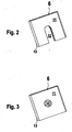
- FIGS 2 and 3 show two embodiments of the receiver 6 of the optoelectronic device 1 according to Figure 1.
- the receiver 6 has a large area, flat photosensitive surface 11 which has a substantially square outer contour.
- the photosensitive surface 11 is homogeneous in the embodiments according to Figures 2 and 3, that is integrally formed.
- the receiver 6 may consist of a number of receiving elements, which each have light-sensitive partial areas, which together form the photosensitive area 11.
- the receiver 6 is mounted on a support 13 which can be connected via connections, not shown, to a circuit board on which the evaluation unit is integrated.
- the cross-sectional area of the carrier 13 is adapted to the size of the photosensitive surface 11.
- the recess 12 extends from the center of the receiver 6 to its lower edge and terminates there.
- the recess 12 is formed by a circular, central bore, which passes through the photosensitive surface 11 and the carrier 13 located behind it.
- the diameter of the recesses are larger than the diameter of the transmitted light beams 3, so that they pass through the recess unhindered.
- the transmitter 4, the transmitting optics 7 and the receiver 6 with the carrier 13 form a structural unit, which are integrated in an opaque insert 14.
- the insert 14 is preferably made of a die-cast zinc part and thus of conductive material, so that this EMC protection for the stored in the interior of electrical or optoelectronic Components forms.
- the insert may be formed by a plastic injection molded part.
- the insert 14 has channel structures, in which the received light beams 5 and the transmitted light beams 3 are guided.
- the channel structures consist of a predetermined number of channels 15a, b, which are bounded by opaque wall elements 16 of the insert 14.
- the channel structures form a honeycomb structure, wherein the channels 15a, b each have a constant cross section.
- the longitudinal axes of the channels 15a, b extend parallel to the optical axes of the transmitter 4 and the receiver 6.
- the channels 15a, b delimiting wall elements 16 of the insert 14 close in front of the photosensitive surface 11 of the receiver 6, which are perpendicular to the longitudinal axes the channels 15a, b are oriented.
- the lengths of the channels 15a, b are dimensioned such that the channel structures are guided as close as possible to the deflection unit, without the scanning of the monitoring area 10 being hindered in this case. Therefore, as shown in Figure 1, the channels 15a, b in the region of the front edge of the polygon mirror 8 shorter than the channels 15a, b in the region of the center of the polygon mirror 8. This ensures that at maximum extent of the channel structures in the direction of the deflection Wall elements 16 of the insert 14 are outside the range of the monitoring area 10, which is swept by the received light beams 5 and transmitted light beams 3.
- the insert 14 significantly increases the detection sensitivity of the optoelectronic device 1. This is due to the fact that through the canary structures the received light beams 5 are almost completely guided by the deflection unit to the receiver 6, but interference and extraneous light radiations are blocked by the insert 14 so that they do not reach the receiver 6.
- the beam axes of the received light beams 5 reflected by the deflection unit run perpendicular to the plane of the photosensitive surface 11, while the interference and external light irradiation from a large angular range in the direction of the receiver 6 is utilized.
- the parallel to the beam axis of the received light beams 5 extending channels 15a, b, the receiving light beams 5 are guided without appreciable reflections on the wall elements 16 of the channel structures to the receiver 6. Since the cross section of the insert 14 is adapted to the size of the photosensitive surface 11, the received light beams 5 are almost completely guided onto the photosensitive surface 11 of the receiver 6.
- the predominantly incident at oblique angles to the channel structures interference and extraneous light rays hit the wall elements 16 of the channel structures and not on the receiver 6. Since the lengths of the channels 15a, b are chosen as large as possible, the interference and extraneous light beams would only after multiple Reflections on the wall elements 16 impinge on the receiver 6.
- the surfaces of the wall elements 16 are strongly light-absorbing. In addition, the surfaces are preferably roughened or structured. Thus, the wall elements 16 act as light traps, so that multiple reflections of interference and extraneous light beams are effectively prevented.
- the honeycomb channel structures have a predetermined number of elongate channels 15a, b with small cross-sectional areas relative to their lengths. This ensures that only such disturbance and Extraneous light rays reach the receiver 6, which extend along the optical axis of the receiver 6 or at a narrow angle thereto.
- FIGS. 4-6 Examples of such channel structures are shown in FIGS. 4-6.
- a plan view of the top side of the insert 14 is shown in FIGS. 4-6.
- the honeycomb structure of the insert 14 according to FIG. 4 corresponds to the insert 14 used in the optoelectronic device 1 according to FIG. 1, in which the transmitter 4 and the receiver 6 are arranged one behind the other.
- a receiver 6 is mounted in the insert 14 according to Figure 4, the photosensitive surface 11 has the shape shown in Figure 2.
- the channel structure of the insert 14 according to Figure 4 has two identically formed, mirror-symmetrically arranged channels 15a, in which the receiving light beams 5 are guided.
- the photosensitive surface 11 of the receiver 6 in the bottom region of the insert 14 is adapted to the geometries of the channels 15a so that it extends over the entire cross-sectional areas of the channels 15a.
- the channel structure of the insert 14 a channel 15 b, which opens at a side wall of the insert 14.
- this channel 15b emitted by the transmitter 4 transmitted light beams 3 are guided.
- the wall element 16 between this channel 15b and the two adjacent channels 15a an optical separation of the transmitted light beams 3 and the received light beams 5 is achieved.
- the beam cross section of the transmitted light beams 3 is smaller than the cross section of the channel 15a, so that in this case the transmitted light beams 3 are guided on the adjacent wall element 16 without reflections.
- FIG. 5 shows a further embodiment of an insert 14 which can be used for the optoelectronic device 1 according to FIG.
- the transmitter 4 and the receiver 6 are in turn arranged one behind the other in the bottom region of the receiver 6.
- the receiver 6 has the shape shown in Figure 3, that is, the transmitted light beams 3 are guided through a central bore in the photosensitive surface 11.
- the geometry of the channel structures of the insert 14 according to FIG. 5 is adapted to this transmitter-receiver structure.
- the insert 14 has four identically formed first channels 15a, in which the receiving light beams 5 extend and are guided to the photosensitive surface 11 of the receiver 6. Furthermore, a second channel 15b is provided with a circular cross section, in which the transmitted light beams 3 extend. The cross-sectional area of this channel 15b is larger than the beam cross section of the transmitted light beams 3 analogously to the exemplary embodiment according to FIG.
- FIG. 6 shows an embodiment of an insert 14 in which a receiver 6 can be introduced whose photosensitive surface 11 extends over the entire cross-sectional area of the interior of the insert 14.
- This insert 14 is suitable for an optoelectronic device 1, in which only the receiver 6 is arranged in the insert 14, whereas the transmitter 4 is located outside the insert 14.
- the insert 14 only channels 15a, in which the receiving light beams 5 are guided.
- the channels 15a are formed identically.
- channels 15a with different cross-sectional geometries can also be provided.
Description
Die Erfindung betrifft eine optoelektronische Vorrichtung gemäß dem Oberbegriff des Anspruchs 1.The invention relates to an optoelectronic device according to the preamble of
Eine derartige optoelektronische Vorrichtung ist aus der DE 198 44 238 A1 bekannt. Diese optoelektronische Vorrichtung dient zur Erfassung von Marken, die insbesondere als Barcodes ausgebildet sind. Die optoelektronische Vorrichtung weist einen Sender mit einer nachgeordneten Sendeoptik und einen Empfänger mit einer vorgeordneten Empfangsoptik auf. Die vom Sender emittierten Sendelichtstrahlen und die von den Marken reflektierten Empfangslichtstrahlen werden über eine Ablenkeinheit geführt. Die Ablenkeinheit besteht aus einem rotierenden Polygonspiegelrad mit einer vorgegebenen Anzahl von Spiegelflächen. Mittels der Ablenkeinheit werden die Sendelichtstrahlen periodisch innerhalb eines Überwachungsbereichs geführt.Such an optoelectronic device is known from DE 198 44 238 A1. This optoelectronic device is used to detect brands, which are designed in particular as barcodes. The optoelectronic device has a transmitter with a downstream transmitting optics and a receiver with an upstream receiving optics. The transmitted light beams emitted by the transmitter and the received light beams reflected by the marks are passed through a deflection unit. The deflection unit consists of a rotating polygon mirror wheel with a predetermined number of mirror surfaces. By means of the deflection unit, the transmitted light beams are periodically guided within a monitoring area.
Um die Sendelichtstrahlen und Empfangslichtstrahlen jeweils über dieselbe Spiegelfläche des Polygonspiegelrads zu führen, sind zwischen dem Sender und der Ablenkeinheit einerseits und zwischen dem Empfänger und der Ablenkeinheit andererseits diverse Umlenkspiegel angeordnet, über welche die Sendelichtstrahlen und Empfangslichtstrahlen geführt werden.In order to guide the transmitted light beams and received light beams respectively over the same mirror surface of the polygon mirror wheel, various deflecting mirrors are arranged between the transmitter and the deflecting unit on the one hand and between the receiver and the deflecting unit, via which the transmitted light beams and received light beams are guided.
Die optoelektronische Vorrichtung weist somit eine Vielzahl von optischen Komponenten auf, über welche die Sendelichtstrahlen und Empfangslichtstrahlen geführt werden müssen.The optoelectronic device thus has a multiplicity of optical components, via which the transmitted light beams and received light beams must be guided.
Die einzelnen Komponenten, insbesondere die Umlenkspiegel, müssen in geeigneter Weise justiert werden. Dadurch entsteht ein unerwünscht hoher Montageaufwand bei der Fertigung der optoelektronischen Vorrichtung. Zudem weist die optoelektronische Vorrichtung eine unerwünscht große Bauform auf, da insbesondere die Anordnung der Umlenkspiegel und der Empfangsoptik vor dem Empfänger einen großen Platzbedarf beansprucht.The individual components, in particular the deflecting mirror, must be adjusted in a suitable manner. This creates an undesirably high assembly costs in the manufacture of the optoelectronic device. In addition, the optoelectronic device has an undesirably large design, since in particular the arrangement of the deflecting mirrors and the receiving optics in front of the receiver requires a large amount of space.
Dabei ist insbesondere nachteilig, dass durch die vorgegebene Brennweite der Empfangsoptik ein großer Abstand zwischen dieser und der Ablenkeinheit vorgesehen werden muss.It is particularly disadvantageous that a large distance between the latter and the deflection unit must be provided by the predetermined focal length of the receiving optics.
Ein weiterer wesentlicher Nachteil derartiger optoelektronischer Vorrichtungen besteht darin, dass durch die großflächige Empfangsoptik unvermeidlich auch ein unerwünscht hoher Anteil von Stör- und Fremdlichteinstrahlungen auf den Empfänger auftrifft, wodurch die Nachweissicherheit der optoelektronischen Vorrichtung beeinträchtigt wird.Another major disadvantage of such optoelectronic devices is that due to the large-area receiving optics unavoidably also an undesirably high proportion of interference and Fremdlichteinstrahlungen impinges on the receiver, whereby the detection reliability of the optoelectronic device is impaired.
Aus der WO 00/16 239 ist eine weitere gattungsgemäße optoelektronische Vorrichtung zur Erfassung von Barcodes bekannt. Bei dieser optoelektronischen Vorrichtung sind der Sender und der Empfänger übereinander liegend in Abstand zueinander angeordnet. Die vom Sender emittierten Sendelichtstrahlen und die von den Marken zurückreflektierten Empfangslichtstrahlen werden über eine Ablenkeinheit geführt. Die Ablenkeinheit ist von einem Polygonspiegelrad gebildet, welches eine vorgegebene Anzahl von Spiegelflächen aufweist. Die Sendelichtstrahlen und Empfangslichtstrahlen werden jeweils über dieselbe Spiegelfläche des Polygonspiegelrades geführt. Dabei sind die Sendelichtstrahlen und Empfangslichtstrahlen räumlich getrennt voneinander geführt, so dass die Sendelichtstrahlen auf das obere Teilsegment der jeweiligen Spiegelfläche des Polygonspiegelrads treffen, während die Empfangslichtstrahlen über das untere Teilsegment derselben Spiegelfläche geführt sind.From WO 00/16 239 a further generic optoelectronic device for detecting barcodes is known. In this optoelectronic device, the transmitter and the receiver are arranged one above the other at a distance from each other. The transmitted light rays emitted by the transmitter and the received light beams reflected back from the marks are passed through a deflection unit. The deflection unit is formed by a polygon mirror wheel having a predetermined number of mirror surfaces. The transmitted light beams and received light beams are respectively guided over the same mirror surface of the polygon mirror wheel. In this case, the transmitted light beams and received light beams are guided spatially separated from each other, so that the transmitted light beams strike the upper sub-segment of the respective mirror surface of the polygon mirror wheel, while the received light beams are guided over the lower sub-segment of the same mirror surface.
Um eine räumliche Trennung der Sendelichtstrahlen und Empfangslichtstrahlen zu erhalten, müssen die Teilsegmente der Spiegelfläche, auf welche die Sendelichtstrahlen und Empfangslichtstrahlen treffen, deutlich voneinander abgesetzt werden.In order to obtain a spatial separation of the transmitted light beams and received light beams, the sub-segments of the mirror surface to which the Transmitted light beams and received light beams meet, clearly offset from each other.
Hierzu muss die Höhe des Polygonspiegelrads gegenüber herkömmlichen Polygonspiegelrädern deutlich vergrößert werden, um die gewünschte Separation der Sende- und Empfangslichtstrahlen zu erhalten. Dies wiederum bedingt eine unerwünschte Vergrößerung der Bauform der optoelektronischen Vorrichtung.For this purpose, the height of the polygon mirror wheel compared to conventional polygon mirror wheels must be significantly increased in order to obtain the desired separation of the transmitted and received light beams. This in turn requires an undesirable increase in the design of the optoelectronic device.
Der Erfindung liegt die Aufgabe zugrunde eine optoelektronische Vorrichtung der eingangs genannten Art so auszubilden, dass diese bei einer möglichst geringen Bauform eine möglichst hohe Nachweissicherheit aufweist.The invention has for its object an optoelectronic device of the type mentioned in such a way that it has the highest possible detection reliability with the smallest possible design.
Zur Lösung dieser Aufgabe sind die Merkmale des Anspruchs 1 vorgesehen. Vorteilhafte Ausführungsformen und zweckmäßigeWeiterbildungen der Erfindung sind in den Unteransprüchen beschrieben.To solve this problem, the features of
Die erfindungsgemäße optoelektronische Vorrichtung dient zur Erfassung von mit Kontrastmustern versehenen Marken und weist einen Sendelichtstrahlen emittierenden Sender, einen Empfangslichtstrahlen empfangenden Empfänger, eine Ablenkeinheit, mittels derer die Sendelichtstrahlen periodisch innerhalb eines Überwachungsbereichs geführt sind, und eine Auswerteeinheit zur Auswertung der am Ausgang des Empfängers anstehenden Empfangssignale auf. Der Empfänger ist in einem lichtundurchlässigen Einsatz gelagert, welcher in Richtung der optischen Achse des Empfängers verlaufende Kanalstrukturen aufweist, in welchen die von der Ablenkeinheit reflektierten Empfangslichtstrahlen zum Empfänger geführt sind.The optoelectronic device according to the invention is used to detect marks provided with contrast patterns and has a transmitting light beam emitting transmitter, a receiving light beam receiving receiver, a deflection unit, by means of which the transmitted light beams are guided periodically within a monitoring area, and an evaluation unit for evaluating the pending at the output of the receiver receive signals on. The receiver is mounted in an opaque insert which has channel structures extending in the direction of the optical axis of the receiver, in which the received light beams reflected by the deflection unit are guided to the receiver.
Ein wesentlicher Vorteil der Erfindung besteht darin, dass der im Einsatz gelagerte Empfänger ohne Zwischenschaltung einer Empfangsoptik und Umlenkspiegeln der Ablenkeinheit gegenüberliegt. Der Abstand zwischen Empfänger und Ablenkeinheit kann somit sehr gering gehalten werden, wodurch die Baugröße der optoelektronischen Vorrichtung entsprechend reduziert ist. Zudem ist dadurch die Anzahl der optischen Komponenten der optoelektronischen Vorrichtung erheblich reduziert, wodurch diese einfach und kostengünstig herstellbar ist.An essential advantage of the invention is that the receiver mounted in the insert is opposite the deflecting unit without the interposition of a receiving optical unit and deflecting mirrors. The distance between the receiver and deflector can thus be kept very low, whereby the size the optoelectronic device is reduced accordingly. In addition, this significantly reduces the number of optical components of the optoelectronic device, as a result of which it is simple and inexpensive to produce.
Ein weiterer wesentlicher Vorteil der erfindungsgemäßen optoelektronischen Vorrichtung besteht darin, dass durch die Führung der Empfangslichtstrahlen in den Kanalstrukturen des Einsatzes die Stör- und Fremdlichteinstrahlung auf den Empfänger wesentlich reduziert ist, wodurch eine hohe Nachweissicherheit der optoelektronischen Vorrichtung erhalten wird.Another important advantage of the optoelectronic device according to the invention is that the interference and external light irradiation to the receiver is substantially reduced by the guidance of the received light beams in the channel structures of the insert, whereby a high detection reliability of the optoelectronic device is obtained.
Dies beruht darauf, dass die Geometrie des Einsatzes an die Strahlführung der Empfangslichtstrahlen dadurch optimal angepasst ist, dass die Kanäle der Kanalstrukturen parallel zur optischen Achse des Empfängers verlaufen. Die entlang der optischen Achse verlaufenden Empfangslichtstrahlen treffen somit nahezu ungehindert auf den Empfänger. Dagegen treffen schräg einfallende Stör- und Fremdlichteinstrahlungen auf die lichtundurchlässigen Wandelemente der Kanalstrukturen, so dass diese nicht mehr auf den Empfänger treffen.This is due to the fact that the geometry of the insert is optimally adapted to the beam guidance of the received light beams in that the channels of the channel structures are parallel to the optical axis of the receiver. The receiving light beams running along the optical axis thus strike the receiver almost unhindered. On the other hand, obliquely incident interfering and extraneous light radiations strike the opaque wall elements of the channel structures, so that they no longer strike the receiver.
Um die Ausblendung der Stör- und Fremdlichteinstrahlung zu optimieren, sind die Kanalstrukturen möglichst lang ausgebildet und reichen bis dicht vor die Ablenkeinheit. Zudem weisen die Kanalstrukturen eine Wabenstruktur mit mehreren Kanälen auf, deren Durchmesser erheblich kleiner sind als deren Längen. Somit ist gewährleistet, dass auch in geringen Winkeln zur optischen Achse des Empfängers einfallende Stör- und Fremdlichtstrahlen auf die Wandelemente der Kanalstrukturen und nicht auf den Empfänger auftreffen.In order to optimize the suppression of interference and extraneous light, the channel structures are as long as possible and reach close to the deflection unit. In addition, the channel structures have a honeycomb structure with a plurality of channels whose diameters are considerably smaller than their lengths. This ensures that incident and extraneous light rays impinge on the wall elements of the channel structures and not on the receiver even at low angles to the optical axis of the receiver.
In einer vorteilhaften Ausführungsform sind die Wandelemente der Kanalstrukturen aufgerauht oder strukturiert und wirken so als Lichtfallen für die Stör- und Fremdlichtstrahlen, das heißt es wird verhindert, dass diese durch Mehrfachreflexionen an den Wandelementen noch zum Empfänger gelangen.In an advantageous embodiment, the wall elements of the channel structures are roughened or structured and thus act as light traps for the interference and extraneous light beams, that is to say they are prevented from reaching the receiver as a result of multiple reflections on the wall elements.
In einer bevorzugten Weiterbildung der Erfindung kann der Einsatz aus leitfähigem Material bestehen, so dass mit diesem zudem ein EMV- (Elektromagnetische Verträglichkeit) Schutz des Empfängers erhalten wird.In a preferred embodiment of the invention, the insert may consist of conductive material, so that with this also an EMC (Electromagnetic Compatibility) protection of the receiver is obtained.
In einer besonders vorteilhaften Ausführungsform der Erfindung verlaufen die Sendelichtstrahlen und Empfangslichtstrahlen koaxial. Hierzu ist der Sender ebenfalls im Einsatz angeordnet und liegt unmittelbar hinter dem Empfänger. Die Sendelichtstrahlen sind durch eine Ausnehmung in der lichtempfindlichen Fläche des Empfängers geführt, wodurch die Sendelichtstrahlen von der lichtempfindlichen Fläche zumindest teilweise umschlossen sind.In a particularly advantageous embodiment of the invention, the transmitted light beams and received light beams extend coaxially. For this purpose, the transmitter is also arranged in use and is located directly behind the receiver. The transmitted light beams are guided through a recess in the photosensitive surface of the receiver, whereby the transmitted light beams are at least partially enclosed by the photosensitive surface.
Die Sendelichtstrahlen und Empfangslichtstrahlen sind in diesem Fall in separaten Kanälen der Kanalstruktur des Einsatzes geführt, wodurch eine nahezu vollständige Trennung der Sendelichtstrahlen und Empfangslichtstrahlen erhalten wird.The transmitted light beams and received light beams are guided in this case in separate channels of the channel structure of the insert, whereby a nearly complete separation of the transmitted light beams and received light beams is obtained.
Zudem weist diese Ausführungsform einen besonders kompakten Aufbau auf.In addition, this embodiment has a particularly compact construction.
Die Erfindung wird im nachstehenden anhand der Zeichnungen erläutert. Es zeigen:
- Figur 1:
- Schematische Darstellung eines Ausführungsbeispiels der erfindungsgemäßen optoelektronischen Vorrichtung.
Figur 2, 3:- Unterschiedliche Ausführungsformen des Empfängers für die optoelektronische Vorrichtung gemäß
Figur 1. - Figuren 4 - 6:
- Unterschiedliche Ausführungsformen der Einsätze für die optoelektronische Vorrichtung gemäß
Figur 1.
- FIG. 1:
- Schematic representation of an embodiment of the optoelectronic device according to the invention.
- 2, 3:
- Different embodiments of the receiver for the optoelectronic device according to FIG. 1.
- FIGS. 4 to 6:
- Different embodiments of the inserts for the optoelectronic device according to FIG. 1.
In Figur 1 ist schematisch der Aufbau einer optoelektronischen Vorrichtung 1 zum Erkennen von mit definierten Kontrastmustern versehenen Marken dargestellt. Prinzipiell können die Marken beliebige Folgen und Formen von aneinander angrenzenden Hell-Dunkelflächen, vorzugsweise Schwarz-Weiß-Flächen, aufweisen. Im Folgenden soll die Erfindung für den Fall erläutert werden, dass die Marken von Barcodes 2 gebildet sind. Die Barcodes 2 bestehen im Wesentlichen aus einer Folge von schwarzen und weißen Strichelementen definierter Länge und Breite.FIG. 1 schematically shows the structure of an
Die optoelektronische Vorrichtung 1 weist einen Sendelichtstrahlen 3 emittierenden Sender 4 und einen Empfangslichtstrahlen 5 empfangenden Empfänger 6 auf. Dem Sender 4, der vorzugsweise von einer Laserdiode gebildet ist, ist eine Sendeoptik 7 zur Fokussierung der Sendelichtstrahlen 3 nachgeordnet.The
Die vom Sender 4 emittierten Sendelichtstrahlen 3 und die von dem Barcode 2 zurückreflektierten Empfangslichtstrahlen 5 sind über eine Ablenkeinheit geführt. Die Ablenkeinheit besteht aus einem motorisch getriebenen Polygonspiegelrad 8 mit einer vorgegebenen Anzahl von facettenförmigen Spiegelflächen 9.The emitted light beams 3 emitted by the transmitter 4 and the received
Durch die Drehbewegung des Polygonspiegelrades 8 werden die Sendelichtstrahlen 3 periodisch in einem Überwachungsbereich 10 geführt, der in einer Abtastebene verläuft. Der Überwachungsbereich 10 erstreckt sich über einen bestimmten Winkelbereich, der durch die Anzahl der Spiegelflächen 9 des Polygonspiegelrades 8 vorgegeben ist.As a result of the rotational movement of the
Die am Ausgang des Empfängers 6 anstehenden Empfangssignale werden in einem nicht dargestellten Verstärker verstärkt und in einer ebenfalls nicht dargestellten Auswerteeinheit ausgewertet.The pending at the output of the
Die Empfangslichtstrahlen 5, die an den Barcodes 2 reflektiert werden, weisen entsprechend der Folge von schwarzen und weißen Strichelementen des Barcodes 2 eine Amplitudenmodulation auf. Die am Ausgang des Empfängers 6 anstehenden Empfangssignale weisen eine entsprechende Amplitudenmodulation auf. Die analogen, amplitudenmodulierten Empfangssignale werden in der Auswerteeinheit mittels einer Schwellwerteinheit bewertet. Dadurch entstehen binäre Signalfolgen, anhand derer durch Vergleich mit abgespeicherten Kontrastmustern von Barcodes 2 die Erkennung des Barcodes 2 erfolgt.The received
Die vom Sender 4 emittierten Sendelichtstrahlen 3, die auf die Ablenkeinheit geführt sind und die von den Marken über die Ablenkeinheit zum Empfänger 6 zurückreflektierten Empfangslichtstrahlen 5 verlaufen bei der Ausführungsform gemäß Figur 1 koaxial.The emitted light beams 3 emitted by the transmitter 4, which are guided onto the deflection unit and the received
Diese koaxiale Strahlführung wird dadurch erreicht, dass die lichtempfindliche Fläche 11 des Empfängers 6, der unmittelbar dem Sender 4 und der Sendeoptik 7 nachgeordnet ist, die Sendelichtstrahlen 3 zumindest teilweise umschließt.This coaxial beam guidance is achieved in that the
Diese Strahlführung wird dadurch erreicht, dass der Empfänger 6 und dessen lichtempfindliche Fläche 11 eine Ausnehmung 12 aufweisen, durch welche die Sendelichtstrahlen 3 geführt sind.This beam guidance is achieved in that the
Der Sender 4 und der Empfänger 6 liegen derart in Abstand zu dem Polygonspiegelrad 8, dass die Sendelichtstrahlen 3 und Empfangslichtstrahlen 5 über dieselbe Spiegelfläche 9 des Polygonspiegelrads 8 geführt sind. Die Spiegelflächen 9 des Polygonspiegelrades 8 sind im vorliegenden Fall senkrecht zu den Strahlachsen der Sendelichtstrahlen 3 und Empfangslichtstrahlen 5 orientiert. Der auf eine Spiegelfläche 9 abgebildete Empfangslichtfleck umschließt zumindest teilweise den auf dieselbe Spiegelfläche 9 abgebildeten Sendelichtfleck der Sendelichtstrahlen 3. Die Spiegelflächen 9 sind an die Geometrien der Sendelichtstrahlen 3 und Empfangslichtstrahlen 5 derart angepasst, dass diese die Spiegelfläche 9 möglichst vollständig ausleuchten.The transmitter 4 and the
Die Figuren 2 und 3 zeigen zwei Ausführungsbeispiele des Empfängers 6 der optoelektronischen Vorrichtung 1 gemäß Figur 1. Der Empfänger 6 weist eine großflächige, ebene lichtempfindliche Fläche 11 auf, die eine im Wesentlichen quadratische Außenkontur aufweist. Die lichtempfindliche Fläche 11 ist bei den Ausführungsbeispielen gemäß den Figuren 2 und 3 homogen, das heißt einstückig ausgebildet. Alternativ kann der Empfänger 6 aus einer Anzahl von Empfangselementen bestehen, welche jeweils lichtempfindliche Teilflächen aufweisen, welche zusammen die lichtempfindliche Fläche 11 bilden.Figures 2 and 3 show two embodiments of the
Der Empfänger 6 ist auf einem Träger 13 montiert, welche über nicht dargestellte Anschlüsse an eine Platine anschließbar ist, auf welcher die Auswerteeinheit integriert ist. Die Querschnittsfläche des Trägers 13 ist an die Größe der lichtempfindlichen Fläche 11 angepasst.The
Bei dem Ausführungsbeispiel gemäß Figur 2 verläuft die Ausnehmung 12 vom Zentrum des Empfängers 6 bis zu dessen unteren Rand und mündet dort aus.In the embodiment shown in Figure 2, the
Bei dem Ausführungsbeispiel gemäß Figur 3 ist die Ausnehmung 12 von einer kreisförmigen, zentralen Bohrung gebildet, welche die lichtempfindliche Fläche 11 und den dahinter liegenden Träger 13 durchsetzt.In the embodiment according to FIG. 3, the
Bei beiden Ausführungsbeispielen sind die Durchmesser der Ausnehmungen größer als die Durchmesser der Sendelichtstrahlen 3, so dass diese ungehindert die Ausnehmung durchsetzen.In both embodiments, the diameter of the recesses are larger than the diameter of the transmitted light beams 3, so that they pass through the recess unhindered.
Der Sender 4, die Sendeoptik 7 sowie der Empfänger 6 mit dem Träger 13 bilden eine Baueinheit, welche in einem lichtundurchlässigen Einsatz 14 integriert sind. Der Einsatz 14 besteht vorzugsweise aus einem Zink-Druckguss-Teil und damit aus leitfähigem Material, so dass dieser einen EMV-Schutz für die in dessen Innenraum gelagerten elektrischen beziehungsweise optoelektronischen Komponenten bildet. Alternativ kann der Einsatz von einem Kunststoff-Spritzteil gebildet sein.The transmitter 4, the transmitting optics 7 and the
Diese Komponenten sind im Bereich des Bodens des Einsatzes 14 angeordnet. Die Querschnittsfläche des Einsatzes 14 ist dabei an die Größe der Fläche des Empfängers 6 angepasst. Der Einsatz 14 weist Kanalstrukturen auf, in welchen die Empfangslichtstrahlen 5 beziehungsweise die Sendelichtstrahlen 3 geführt sind. Die Kanalstrukturen bestehen aus einer vorgegebenen Anzahl von Kanälen 15a, b, die durch lichtundurchlässige Wandelemente 16 des Einsatzes 14 begrenzt sind.These components are arranged in the region of the bottom of the
Die Kanalstrukturen bilden eine Wabenstruktur, wobei die Kanäle 15a, b jeweils einen konstanten Querschnitt aufweisen. Die Längsachsen der Kanäle 15a, b verlaufen parallel zu den optischen Achsen des Senders 4 und des Empfängers 6. Dabei enden die die Kanäle 15a, b begrenzenden Wandelemente 16 des Einsatzes 14 dicht vor der lichtempfindlichen Fläche 11 des Empfängers 6, die senkrecht zu den Längsachsen der Kanäle 15a, b orientiert sind.The channel structures form a honeycomb structure, wherein the
Die Längen der Kanäle 15a, b sind so dimensioniert, dass die Kanalstrukturen möglichst dicht bis zur Ablenkeinheit geführt sind, ohne dass hierbei die Abtastung des Überwachungsbereichs 10 behindert wird. Daher sind wie in Figur 1 dargestellt die Kanäle 15a, b im Bereich des vorderen Randes des Polygonspiegelrades 8 kürzer als die Kanäle 15a, b im Bereich des Zentrums des Polygonspiegelrades 8. Damit ist gewährleistet, dass bei maximaler Ausdehnung der Kanalstrukturen in Richtung der Ablenkeinheit die Wandelemente 16 des Einsatzes 14 außerhalb des Bereichs des Überwachungsbereichs 10 liegen, welcher von den Empfangslichtstrahlen 5 und Sendelichtstrahlen 3 überstrichen wird.The lengths of the
Durch den Einsatz 14 wird die Nachweisempfindlichkeit der optoelektronischen Vorrichtung 1 erheblich erhöht. Dies beruht darauf, dass durch die Kanaistrukturen die Empfangslichtstrahlen 5 nahezu vollständig von der Ablenkeinheit zum Empfänger 6 geführt sind, jedoch Stör- und Fremdlichteinstrahlungen durch den Einsatz 14 blockiert werden, so dass diese nicht zum Empfänger 6 gelangen.The
Dabei wird der Umstand ausgenutzt, dass die Strahlachsen der von der Ablenkeinheit reflektierten Empfangslichtstrahlen 5 senkrecht zur Ebene der lichtempfindlichen Fläche 11 verlaufen, während die Stör- und Fremdlichteinstrahlung aus einem großen Winkelbereich in Richtung des Empfängers 6 erfolgt. Durch die parallel zur Strahlachse der Empfangslichtstrahlen 5 verlaufenden Kanäle 15a, b werden die Empfangslichtstrahlen 5 ohne nennenswerte Reflexionen an den Wandelementen 16 der Kanalstrukturen zum Empfänger 6 geführt. Da der Querschnitt des Einsatzes 14 an die Größe der lichtempfindlichen Fläche 11 angepasst ist, werden die Empfangslichtstrahlen 5 nahezu vollständig auf die lichtempfindliche Fläche 11 des Empfängers 6 geführt.The fact that the beam axes of the received
Die überwiegend in schrägen Winkeln auf die Kanalstrukturen auftreffenden Stör- und Fremdlichtstrahlen treffen dagegen auf die Wandelemente 16 der Kanalstrukturen und nicht auf den Empfänger 6. Da die Längen der Kanäle 15a, b möglichst groß gewählt sind, würden die Stör- und Fremdlichtstrahlen erst nach mehrfachen Reflexionen an den Wandelementen 16 auf den Empfänger 6 auftreffen. Die Oberflächen der Wandelemente 16 sind jedoch stark lichtabsorbierend. Zudem sind die Oberflächen vorzugsweise aufgerauht oder strukturiert. Damit wirken die Wandelemente 16 als Lichtfallen, so dass Mehrfachreflexionen von Stör- und Fremdlichtstrahlen effizient unterbunden werden.The predominantly incident at oblique angles to the channel structures interference and extraneous light rays, however, hit the
Die wabenförmige Kanalstrukturen weisen eine vorgegebenen Anzahl von langgestreckten Kanälen 15a, b mit in Verhältnis zu deren Längen kleinen Querschnittsflächen auf. Damit ist gewährleistet, dass nur solche Stör- und Fremdlichtstrahlen zum Empfänger 6 gelangen, die entlang der optische Achse des Empfängers 6 oder in einem eng begrenzten Winkel hierzu verlaufen.The honeycomb channel structures have a predetermined number of
Beispiele für derartige Kanalstrukturen sind in den Figuren 4 - 6 dargestellt. Dabei ist in den Figuren 4 - 6 jeweils eine Draufsicht auf die Oberseite des Einsatzes 14 dargestellt.Examples of such channel structures are shown in FIGS. 4-6. In this case, a plan view of the top side of the
Die Wabenstruktur des Einsatzes 14 gemäß Figur 4 entspricht dem bei der optoelektronischen Vorrichtung 1 gemäß Figur 1 verwendeten Einsatz 14, in welchem der Sender 4 und der Empfänger 6 hintereinander liegend angeordnet sind. Dabei ist in dem Einsatz 14 gemäß Figur 4 ein Empfänger 6 gelagert, dessen lichtempfindliche Fläche 11 die in Figur 2 dargestellte Form aufweist.The honeycomb structure of the
Die Kanalstruktur des Einsatzes 14 gemäß Figur 4 weist zwei identisch ausgebildete, spiegelsymmetrisch angeordnete Kanäle 15a auf, in welchen die Empfangslichtstrahlen 5 geführt sind. Die lichtempfindliche Fläche 11 des Empfängers 6 im Bodenbereich des Einsatzes 14 ist an die Geometrien der Kanäle 15a angepasst, so dass sich diese über die gesamten Querschnittsflächen der Kanäle 15a erstreckt.The channel structure of the
Weiterhin weist die Kanalstruktur des Einsatzes 14 einen Kanal 15b auf, der an einer Seitenwand des Einsatzes 14 ausmündet. In diesem Kanal 15b sind die vom Sender 4 emittierten Sendelichtstrahlen 3 geführt. Durch das Wandelement 16 zwischen diesem Kanal 15b und den beiden angrenzenden Kanälen 15a wird eine optische Trennung der Sendelichtstrahlen 3 und der Empfangslichtstrahlen 5 erreicht. Wie aus Figur 4 ersichtlich ist der Strahlquerschnitt der Sendelichtstrahlen 3 kleiner als der Querschnitt des Kanals 15a, so dass in diesem die Sendelichtstrahlen 3 ohne Reflexionen am angrenzenden Wandelement 16 geführt sind.Furthermore, the channel structure of the insert 14 a
Figur 5 zeigt eine weitere Ausführungsform eines Einsatzes 14, der für die optoelektronische Vorrichtung 1 gemäß Figur 1 einsetzbar ist. Der Sender 4 und der Empfänger 6 sind wiederum hintereinander im Bodenbereich des Empfängers 6 angeordnet. Im vorliegenden Fall weist der Empfänger 6 die in Figur 3 dargestellte Form auf, das heißt die Sendelichtstrahlen 3 sind durch eine zentrale Bohrung in der lichtempfindlichen Fläche 11 geführt. Die Geometrie der Kanalstrukturen des Einsatzes 14 gemäß Figur 5 ist an diese Sender-Empfängerstruktur angepasst.FIG. 5 shows a further embodiment of an
Der Einsatz 14 weist vier identisch ausgebildete erste Kanäle 15a auf, in welchen die Empfangslichtstrahlen 5 verlaufen und zur lichtempfindlichen Fläche 11 des Empfängers 6 geführt sind. Weiterhin ist ein zweiter Kanal 15b mit einem kreisförmigen Querschnitt vorgesehen, in welchen die Sendelichtstrahlen 3 verlaufen. Die Querschnittsfläche dieses Kanals 15b ist analog zu dem Ausführungsbeispiel gemäß Figur 4 größer als der Strahlquerschnitt der Sendelichtstrahlen 3.The
Figur 6 zeigt eine Ausführungsform eines Einsatzes 14, in welchem ein Empfänger 6 einbringbar ist, dessen lichtempfindliche Fläche 11 sich über die gesamte Querschnittsfläche des Innenraumes des Einsatzes 14 erstreckt.FIG. 6 shows an embodiment of an
Dieser Einsatz 14 ist für eine optoelektronische Vorrichtung 1 geeignet, bei welcher nur der Empfänger 6 im Einsatz 14 angeordnet ist, wogegen der Sender 4 außerhalb des Einsatzes 14 liegt.This
In diesem Fall weist der Einsatz 14 nur Kanäle 15a auf, in welchen die Empfangslichtstrahlen 5 geführt sind. Wie aus Figur 6 ersichtlich, sind die Kanäle 15a identisch ausgebildet. Prinzipiell können auch Kanäle 15a mit unterschiedlichen Querschnittsgeometrien vorgesehen sein.
Leuze electronic GmbH + Co.
73277 Owen/Teck, DEIn this case, the
Leuze electronic GmbH + Co.
73277 Owen / Teck, DE
- (1)(1)
- Optoelektronische VorrichtungOptoelectronic device
- (2)(2)
- Barcodesbarcodes
- (3)(3)
- SendelichtstrahlenTransmitted light beams
- (4)(4)
- Sendertransmitter
- (5)(5)
- EmpfangslichtstrahlenReceiving light rays
- (6)(6)
- Empfängerreceiver
- (7)(7)
- Sendeoptiktransmission optics
- (8)(8th)
- Polygonspiegelradpolygonal
- (9)(9)
- Spiegelflächemirror surface
- (10)(10)
- Überwachungsbereichmonitoring area
- (11)(11)
- Lichtempfindliche FlächePhotosensitive surface
- (12)(12)
- Ausnehmungrecess
- (13)(13)
- Trägercarrier
- (14)(14)
- Einsatzcommitment
- (15a)(15a)
- Kanalchannel
- (15b)(15b)
- Kanalchannel
- (16)(16)
- Wandelementwall element
Claims (17)
- Optoelectronic device for detection of marks provided with contrast patterns, comprising a transmitter emitting transmitted light beams, a receiver receiving received light beams, a deflecting unit by means of which the transmitted light beams are periodically guided within a monitoring region, and an evaluating unit for evaluation of the received signals present at the output of the receiver, characterised in that the receiver (6) is mounted in a light-impervious insert (14) having channel structures which extend in the direction of the optical axis of the receiver (6) and in which the received light beams (5) reflected by the deflecting unit are guided to the receiver (6).
- Optoelectronic device according to claim 1, characterised in that the receiver (6) is arranged in the base region of the insert (14) and that the channel structures have channels (15a, b) which are bounded by wall elements (16) protruding perpendicularly from the base of the insert (14).
- Optoelectronic device according to claim 2, characterised in that the channel structures have a honeycomb structure, the channels (15a, 15b) of which extend perpendicularly to the optical axis of the receiver (6).
- Optoelectronic device according to one of claims 2 and 3, characterised in that the cross-sectional area of the insert (14) is adapted to the size of the light-sensitive surface (11) of the receiver (6).
- Optoelectronic device according to claim 4, characterised in that the receiver (6) has a homogeneous, cohesive light-sensitive surface (11).
- Optoelectronic device according to claim 4, characterised in that the receiver (6) consists of a predetermined-number of receiving elements, the light-sensitive part surfaces of which are components of the light-sensitive surface (11).
- Optoelectronic device according to one of claims 2 to 6, characterised in that the wall elements (16) of the channel structure have roughened or structured surfaces.
- Optoelectronic device according to one of claims 1 to 7, characterised in that the insert (14) consists of a metal diecast part or of a plastics material injection-moulded part.
- Optoelectronic device according to one of claims 1 to 8, characterised in that the insert (14) consists of electrically conductive material.
- Optoelectronic device according to one of claims 1 to 9, characterised in that the transmitter (4) and the receiver (6) are arranged in the insert (14).
- Optoelectronic device according to claim 10, characterised in that the transmitted light beams (3) and received light beams (5) are guided to extend coaxially over the deflecting unit.
- Optoelectronic device according to claim 11, characterised in that the light-sensitive surface (11) of the receiver (6) at least partly encloses the transmitted light beams (3).
- Optoelectronic device according to one of claims 11 and 12, characterised in that the light-sensitive surface (11) of the receiver (6) has a recess and that the transmitter (4) is arranged behind the receiver (6) so that the transmitted light beams (3) are guided through the recess.
- Optoelectronic device according to claim 13, characterised in that the recess is formed as a central bore in the light-sensitive surface (11) of the receiver (6).
- Optoelectronic device according to claim 14, characterised in that the recess opens at an edge of the receiver (6).
- Optoelectronic device according to one of claims 10 to 15, characterised in that the transmitted light beams (3) and received light beams (5) are guided in separate channels (15a, b) of the channel structures of the insert (14).
- Optoelectronic device according to one of claims 1 to 16, characterised in that the deflecting unit is formed by a polygon mirror wheel (8) with a predetermined number of mirror surfaces (9), wherein the received light spot, which is imaged on a mirror surface (9), of the received light beams (5) at least partly encloses the transmitted light spot imaged on the same mirror surface (9).
Applications Claiming Priority (2)
| Application Number | Priority Date | Filing Date | Title |
|---|---|---|---|
| DE10209269A DE10209269C1 (en) | 2002-03-01 | 2002-03-01 | Optoelectronic device for detecting barcode markings has receiver enclosed by light shield with channel structure allowing passage of light reflected by beam deflection device |
| DE10209269 | 2002-03-01 |
Publications (2)
| Publication Number | Publication Date |
|---|---|
| EP1341118A1 EP1341118A1 (en) | 2003-09-03 |
| EP1341118B1 true EP1341118B1 (en) | 2006-09-06 |
Family
ID=7713996
Family Applications (1)
| Application Number | Title | Priority Date | Filing Date |
|---|---|---|---|
| EP03003883A Expired - Lifetime EP1341118B1 (en) | 2002-03-01 | 2003-02-21 | Optoelectronic device |
Country Status (4)
| Country | Link |
|---|---|
| US (1) | US6817526B2 (en) |
| EP (1) | EP1341118B1 (en) |
| JP (1) | JP4375977B2 (en) |
| DE (2) | DE10209269C1 (en) |
Families Citing this family (1)
| Publication number | Priority date | Publication date | Assignee | Title |
|---|---|---|---|---|
| DE102008053881A1 (en) * | 2008-10-30 | 2010-05-12 | I.L.E.E. Ag Industrial Laser And Electronic Engineering | Reflection barrier with surveying and / or localization function |
Family Cites Families (9)
| Publication number | Priority date | Publication date | Assignee | Title |
|---|---|---|---|---|
| US4916318A (en) * | 1986-12-16 | 1990-04-10 | Asahi Kogaku Kogyo K.K. | Scan type optical reader with changing beam waist position |
| EP0572685B1 (en) * | 1992-05-18 | 1998-08-12 | Sumitomo Electric Industries, Ltd. | A symbol reading device for varying the focal point of a scanning laser beam through variance of scanning laser beam optical path length |
| DE69725031T2 (en) * | 1996-01-27 | 2009-02-05 | Datalogic S.P.A., Lippo Di Calderara Di Reno | sampler |
| US6075883A (en) * | 1996-11-12 | 2000-06-13 | Robotic Vision Systems, Inc. | Method and system for imaging an object or pattern |
| EP0926615B1 (en) * | 1997-12-16 | 2001-05-09 | Datalogic S.P.A. | An optical code scanning reader with laser beams travelling along a minimum of two different optical paths |
| DE19845946C1 (en) * | 1998-08-21 | 1999-08-12 | Leuze Electronic Gmbh & Co | Optoelectronic arrangement for detecting markers with defined contrast patterns |
| US6808115B2 (en) * | 1998-09-11 | 2004-10-26 | Accu-Sort Systems, Inc. | Quasi-coaxial optical bar code reader |
| DE19844238C2 (en) * | 1998-09-26 | 2003-11-13 | Leuze Electronic Gmbh & Co Kg | Optoelectronic device |
| US6481628B2 (en) * | 2001-04-10 | 2002-11-19 | Kenneth Liou | Pen-type barcode scanner |
-
2002
- 2002-03-01 DE DE10209269A patent/DE10209269C1/en not_active Expired - Fee Related
-
2003
- 2003-02-21 DE DE50304910T patent/DE50304910D1/en not_active Expired - Lifetime
- 2003-02-21 EP EP03003883A patent/EP1341118B1/en not_active Expired - Lifetime
- 2003-02-28 JP JP2003054273A patent/JP4375977B2/en not_active Expired - Lifetime
- 2003-07-16 US US10/619,568 patent/US6817526B2/en not_active Expired - Fee Related
Also Published As
| Publication number | Publication date |
|---|---|
| US6817526B2 (en) | 2004-11-16 |
| DE10209269C1 (en) | 2003-07-03 |
| DE50304910D1 (en) | 2006-10-19 |
| JP2003262820A (en) | 2003-09-19 |
| EP1341118A1 (en) | 2003-09-03 |
| US20040011870A1 (en) | 2004-01-22 |
| JP4375977B2 (en) | 2009-12-02 |
Similar Documents
| Publication | Publication Date | Title |
|---|---|---|
| DE19850270B4 (en) | Optoelectronic device | |
| EP0708928A1 (en) | Process for detecting objects in a monitoring region | |
| DE19732776C1 (en) | Optoelectronic device for detecting object in surveillance zone | |
| EP3388857B1 (en) | Laser scanner and method for testing its functional capability | |
| EP1921565B1 (en) | Bar code reader | |
| DE102005010657A1 (en) | Object detecting device | |
| EP1666913B1 (en) | Optical sensor | |
| EP1845334A1 (en) | Optical sensor | |
| EP1160718B1 (en) | Laser scanner | |
| EP2159599B1 (en) | Optoelectronic sensor | |
| EP1207491B1 (en) | Optoelectronic device | |
| WO1999052751A1 (en) | Sensor device for detecting moisture on a window | |
| WO1999052752A1 (en) | Sensor device for detecting moisture on a window | |
| EP1341118B1 (en) | Optoelectronic device | |
| EP1102086B1 (en) | Opto-electronic device | |
| EP2226654B1 (en) | Optical sensor | |
| EP3070496A1 (en) | Polygon scanner and method for recording objects | |
| DE10205294B4 (en) | Optoelectronic device | |
| EP3312760B1 (en) | Optical sensor | |
| EP1324003A2 (en) | Steering angle sensor | |
| DE19844238C2 (en) | Optoelectronic device | |
| EP1134545A1 (en) | Distance sensor | |
| DE19844234C2 (en) | Optoelectronic device | |
| DE19845946C1 (en) | Optoelectronic arrangement for detecting markers with defined contrast patterns | |
| EP1496335A2 (en) | Optoelectronic device |
Legal Events
| Date | Code | Title | Description |
|---|---|---|---|
| PUAI | Public reference made under article 153(3) epc to a published international application that has entered the european phase |
Free format text: ORIGINAL CODE: 0009012 |
|
| 17P | Request for examination filed |
Effective date: 20030312 |
|
| AK | Designated contracting states |
Kind code of ref document: A1 Designated state(s): AT BE BG CH CY CZ DE DK EE ES FI FR GB GR HU IE IT LI LU MC NL PT SE SI SK TR |
|
| AX | Request for extension of the european patent |
Extension state: AL LT LV MK RO |
|
| AKX | Designation fees paid |
Designated state(s): CH DE FR GB IT LI NL |
|
| GRAP | Despatch of communication of intention to grant a patent |
Free format text: ORIGINAL CODE: EPIDOSNIGR1 |
|
| GRAS | Grant fee paid |
Free format text: ORIGINAL CODE: EPIDOSNIGR3 |
|
| GRAA | (expected) grant |
Free format text: ORIGINAL CODE: 0009210 |
|
| RAP1 | Party data changed (applicant data changed or rights of an application transferred) |
Owner name: LEUZE ELECTRONIC GMBH + CO. KG |
|
| AK | Designated contracting states |
Kind code of ref document: B1 Designated state(s): CH DE FR GB IT LI NL |
|
| PG25 | Lapsed in a contracting state [announced via postgrant information from national office to epo] |
Ref country code: IT Free format text: LAPSE BECAUSE OF FAILURE TO SUBMIT A TRANSLATION OF THE DESCRIPTION OR TO PAY THE FEE WITHIN THE PRESCRIBED TIME-LIMIT;WARNING: LAPSES OF ITALIAN PATENTS WITH EFFECTIVE DATE BEFORE 2007 MAY HAVE OCCURRED AT ANY TIME BEFORE 2007. THE CORRECT EFFECTIVE DATE MAY BE DIFFERENT FROM THE ONE RECORDED. Effective date: 20060906 |
|
| REG | Reference to a national code |
Ref country code: GB Ref legal event code: FG4D Free format text: NOT ENGLISH |
|
| REG | Reference to a national code |
Ref country code: CH Ref legal event code: NV Representative=s name: ROTTMANN, ZIMMERMANN + PARTNER AG Ref country code: CH Ref legal event code: EP |
|
| REF | Corresponds to: |
Ref document number: 50304910 Country of ref document: DE Date of ref document: 20061019 Kind code of ref document: P |
|
| GBT | Gb: translation of ep patent filed (gb section 77(6)(a)/1977) |
Effective date: 20061003 |
|
| ET | Fr: translation filed | ||
| PLBE | No opposition filed within time limit |
Free format text: ORIGINAL CODE: 0009261 |
|
| STAA | Information on the status of an ep patent application or granted ep patent |
Free format text: STATUS: NO OPPOSITION FILED WITHIN TIME LIMIT |
|
| 26N | No opposition filed |
Effective date: 20070607 |
|
| REG | Reference to a national code |
Ref country code: CH Ref legal event code: PFA Owner name: LEUZE ELECTRONIC GMBH + CO. KG Free format text: LEUZE ELECTRONIC GMBH + CO. KG#IN DER BRAIKE 1#73277 OWEN/TECK (DE) -TRANSFER TO- LEUZE ELECTRONIC GMBH + CO. KG#IN DER BRAIKE 1#73277 OWEN/TECK (DE) |
|
| PGFP | Annual fee paid to national office [announced via postgrant information from national office to epo] |
Ref country code: DE Payment date: 20130312 Year of fee payment: 11 |
|
| PGFP | Annual fee paid to national office [announced via postgrant information from national office to epo] |
Ref country code: NL Payment date: 20140218 Year of fee payment: 12 Ref country code: CH Payment date: 20140218 Year of fee payment: 12 |
|
| PGFP | Annual fee paid to national office [announced via postgrant information from national office to epo] |
Ref country code: FR Payment date: 20140219 Year of fee payment: 12 Ref country code: IT Payment date: 20140224 Year of fee payment: 12 |
|
| PGFP | Annual fee paid to national office [announced via postgrant information from national office to epo] |
Ref country code: GB Payment date: 20140218 Year of fee payment: 12 |
|
| REG | Reference to a national code |
Ref country code: DE Ref legal event code: R119 Ref document number: 50304910 Country of ref document: DE |
|
| REG | Reference to a national code |
Ref country code: DE Ref legal event code: R119 Ref document number: 50304910 Country of ref document: DE Effective date: 20140902 |
|
| PG25 | Lapsed in a contracting state [announced via postgrant information from national office to epo] |
Ref country code: DE Free format text: LAPSE BECAUSE OF NON-PAYMENT OF DUE FEES Effective date: 20140902 |
|
| REG | Reference to a national code |
Ref country code: NL Ref legal event code: V1 Effective date: 20150901 |
|
| PG25 | Lapsed in a contracting state [announced via postgrant information from national office to epo] |
Ref country code: NL Free format text: LAPSE BECAUSE OF NON-PAYMENT OF DUE FEES Effective date: 20150901 |
|
| REG | Reference to a national code |
Ref country code: CH Ref legal event code: PL |
|
| GBPC | Gb: european patent ceased through non-payment of renewal fee |
Effective date: 20150221 |
|
| PG25 | Lapsed in a contracting state [announced via postgrant information from national office to epo] |
Ref country code: CH Free format text: LAPSE BECAUSE OF NON-PAYMENT OF DUE FEES Effective date: 20150228 Ref country code: LI Free format text: LAPSE BECAUSE OF NON-PAYMENT OF DUE FEES Effective date: 20150228 |
|
| REG | Reference to a national code |
Ref country code: FR Ref legal event code: ST Effective date: 20151030 |
|
| PG25 | Lapsed in a contracting state [announced via postgrant information from national office to epo] |
Ref country code: IT Free format text: LAPSE BECAUSE OF NON-PAYMENT OF DUE FEES Effective date: 20150221 |
|
| PG25 | Lapsed in a contracting state [announced via postgrant information from national office to epo] |
Ref country code: GB Free format text: LAPSE BECAUSE OF NON-PAYMENT OF DUE FEES Effective date: 20150221 |
|
| PG25 | Lapsed in a contracting state [announced via postgrant information from national office to epo] |
Ref country code: FR Free format text: LAPSE BECAUSE OF NON-PAYMENT OF DUE FEES Effective date: 20150302 |
|
| P01 | Opt-out of the competence of the unified patent court (upc) registered |
Effective date: 20231018 |