EP1336952A2 - Method for driving a plasma display panel improving luminance - Google Patents
Method for driving a plasma display panel improving luminance Download PDFInfo
- Publication number
- EP1336952A2 EP1336952A2 EP03250115A EP03250115A EP1336952A2 EP 1336952 A2 EP1336952 A2 EP 1336952A2 EP 03250115 A EP03250115 A EP 03250115A EP 03250115 A EP03250115 A EP 03250115A EP 1336952 A2 EP1336952 A2 EP 1336952A2
- Authority
- EP
- European Patent Office
- Prior art keywords
- display
- electrode
- discharge
- time point
- electrodes
- Prior art date
- Legal status (The legal status is an assumption and is not a legal conclusion. Google has not performed a legal analysis and makes no representation as to the accuracy of the status listed.)
- Withdrawn
Links
Images







Classifications
-
- G—PHYSICS
- G09—EDUCATION; CRYPTOGRAPHY; DISPLAY; ADVERTISING; SEALS
- G09G—ARRANGEMENTS OR CIRCUITS FOR CONTROL OF INDICATING DEVICES USING STATIC MEANS TO PRESENT VARIABLE INFORMATION
- G09G3/00—Control arrangements or circuits, of interest only in connection with visual indicators other than cathode-ray tubes
- G09G3/20—Control arrangements or circuits, of interest only in connection with visual indicators other than cathode-ray tubes for presentation of an assembly of a number of characters, e.g. a page, by composing the assembly by combination of individual elements arranged in a matrix no fixed position being assigned to or needed to be assigned to the individual characters or partial characters
- G09G3/22—Control arrangements or circuits, of interest only in connection with visual indicators other than cathode-ray tubes for presentation of an assembly of a number of characters, e.g. a page, by composing the assembly by combination of individual elements arranged in a matrix no fixed position being assigned to or needed to be assigned to the individual characters or partial characters using controlled light sources
- G09G3/28—Control arrangements or circuits, of interest only in connection with visual indicators other than cathode-ray tubes for presentation of an assembly of a number of characters, e.g. a page, by composing the assembly by combination of individual elements arranged in a matrix no fixed position being assigned to or needed to be assigned to the individual characters or partial characters using controlled light sources using luminous gas-discharge panels, e.g. plasma panels
- G09G3/288—Control arrangements or circuits, of interest only in connection with visual indicators other than cathode-ray tubes for presentation of an assembly of a number of characters, e.g. a page, by composing the assembly by combination of individual elements arranged in a matrix no fixed position being assigned to or needed to be assigned to the individual characters or partial characters using controlled light sources using luminous gas-discharge panels, e.g. plasma panels using AC panels
- G09G3/298—Control arrangements or circuits, of interest only in connection with visual indicators other than cathode-ray tubes for presentation of an assembly of a number of characters, e.g. a page, by composing the assembly by combination of individual elements arranged in a matrix no fixed position being assigned to or needed to be assigned to the individual characters or partial characters using controlled light sources using luminous gas-discharge panels, e.g. plasma panels using AC panels using surface discharge panels
- G09G3/2983—Control arrangements or circuits, of interest only in connection with visual indicators other than cathode-ray tubes for presentation of an assembly of a number of characters, e.g. a page, by composing the assembly by combination of individual elements arranged in a matrix no fixed position being assigned to or needed to be assigned to the individual characters or partial characters using controlled light sources using luminous gas-discharge panels, e.g. plasma panels using AC panels using surface discharge panels using non-standard pixel electrode arrangements
-
- G—PHYSICS
- G09—EDUCATION; CRYPTOGRAPHY; DISPLAY; ADVERTISING; SEALS
- G09G—ARRANGEMENTS OR CIRCUITS FOR CONTROL OF INDICATING DEVICES USING STATIC MEANS TO PRESENT VARIABLE INFORMATION
- G09G3/00—Control arrangements or circuits, of interest only in connection with visual indicators other than cathode-ray tubes
- G09G3/20—Control arrangements or circuits, of interest only in connection with visual indicators other than cathode-ray tubes for presentation of an assembly of a number of characters, e.g. a page, by composing the assembly by combination of individual elements arranged in a matrix no fixed position being assigned to or needed to be assigned to the individual characters or partial characters
- G09G3/22—Control arrangements or circuits, of interest only in connection with visual indicators other than cathode-ray tubes for presentation of an assembly of a number of characters, e.g. a page, by composing the assembly by combination of individual elements arranged in a matrix no fixed position being assigned to or needed to be assigned to the individual characters or partial characters using controlled light sources
- G09G3/28—Control arrangements or circuits, of interest only in connection with visual indicators other than cathode-ray tubes for presentation of an assembly of a number of characters, e.g. a page, by composing the assembly by combination of individual elements arranged in a matrix no fixed position being assigned to or needed to be assigned to the individual characters or partial characters using controlled light sources using luminous gas-discharge panels, e.g. plasma panels
- G09G3/288—Control arrangements or circuits, of interest only in connection with visual indicators other than cathode-ray tubes for presentation of an assembly of a number of characters, e.g. a page, by composing the assembly by combination of individual elements arranged in a matrix no fixed position being assigned to or needed to be assigned to the individual characters or partial characters using controlled light sources using luminous gas-discharge panels, e.g. plasma panels using AC panels
- G09G3/291—Control arrangements or circuits, of interest only in connection with visual indicators other than cathode-ray tubes for presentation of an assembly of a number of characters, e.g. a page, by composing the assembly by combination of individual elements arranged in a matrix no fixed position being assigned to or needed to be assigned to the individual characters or partial characters using controlled light sources using luminous gas-discharge panels, e.g. plasma panels using AC panels controlling the gas discharge to control a cell condition, e.g. by means of specific pulse shapes
-
- G—PHYSICS
- G09—EDUCATION; CRYPTOGRAPHY; DISPLAY; ADVERTISING; SEALS
- G09G—ARRANGEMENTS OR CIRCUITS FOR CONTROL OF INDICATING DEVICES USING STATIC MEANS TO PRESENT VARIABLE INFORMATION
- G09G3/00—Control arrangements or circuits, of interest only in connection with visual indicators other than cathode-ray tubes
- G09G3/20—Control arrangements or circuits, of interest only in connection with visual indicators other than cathode-ray tubes for presentation of an assembly of a number of characters, e.g. a page, by composing the assembly by combination of individual elements arranged in a matrix no fixed position being assigned to or needed to be assigned to the individual characters or partial characters
- G09G3/22—Control arrangements or circuits, of interest only in connection with visual indicators other than cathode-ray tubes for presentation of an assembly of a number of characters, e.g. a page, by composing the assembly by combination of individual elements arranged in a matrix no fixed position being assigned to or needed to be assigned to the individual characters or partial characters using controlled light sources
- G09G3/28—Control arrangements or circuits, of interest only in connection with visual indicators other than cathode-ray tubes for presentation of an assembly of a number of characters, e.g. a page, by composing the assembly by combination of individual elements arranged in a matrix no fixed position being assigned to or needed to be assigned to the individual characters or partial characters using controlled light sources using luminous gas-discharge panels, e.g. plasma panels
- G09G3/288—Control arrangements or circuits, of interest only in connection with visual indicators other than cathode-ray tubes for presentation of an assembly of a number of characters, e.g. a page, by composing the assembly by combination of individual elements arranged in a matrix no fixed position being assigned to or needed to be assigned to the individual characters or partial characters using controlled light sources using luminous gas-discharge panels, e.g. plasma panels using AC panels
- G09G3/291—Control arrangements or circuits, of interest only in connection with visual indicators other than cathode-ray tubes for presentation of an assembly of a number of characters, e.g. a page, by composing the assembly by combination of individual elements arranged in a matrix no fixed position being assigned to or needed to be assigned to the individual characters or partial characters using controlled light sources using luminous gas-discharge panels, e.g. plasma panels using AC panels controlling the gas discharge to control a cell condition, e.g. by means of specific pulse shapes
- G09G3/294—Control arrangements or circuits, of interest only in connection with visual indicators other than cathode-ray tubes for presentation of an assembly of a number of characters, e.g. a page, by composing the assembly by combination of individual elements arranged in a matrix no fixed position being assigned to or needed to be assigned to the individual characters or partial characters using controlled light sources using luminous gas-discharge panels, e.g. plasma panels using AC panels controlling the gas discharge to control a cell condition, e.g. by means of specific pulse shapes for lighting or sustain discharge
- G09G3/2942—Control arrangements or circuits, of interest only in connection with visual indicators other than cathode-ray tubes for presentation of an assembly of a number of characters, e.g. a page, by composing the assembly by combination of individual elements arranged in a matrix no fixed position being assigned to or needed to be assigned to the individual characters or partial characters using controlled light sources using luminous gas-discharge panels, e.g. plasma panels using AC panels controlling the gas discharge to control a cell condition, e.g. by means of specific pulse shapes for lighting or sustain discharge with special waveforms to increase luminous efficiency
-
- G—PHYSICS
- G09—EDUCATION; CRYPTOGRAPHY; DISPLAY; ADVERTISING; SEALS
- G09G—ARRANGEMENTS OR CIRCUITS FOR CONTROL OF INDICATING DEVICES USING STATIC MEANS TO PRESENT VARIABLE INFORMATION
- G09G3/00—Control arrangements or circuits, of interest only in connection with visual indicators other than cathode-ray tubes
- G09G3/20—Control arrangements or circuits, of interest only in connection with visual indicators other than cathode-ray tubes for presentation of an assembly of a number of characters, e.g. a page, by composing the assembly by combination of individual elements arranged in a matrix no fixed position being assigned to or needed to be assigned to the individual characters or partial characters
- G09G3/22—Control arrangements or circuits, of interest only in connection with visual indicators other than cathode-ray tubes for presentation of an assembly of a number of characters, e.g. a page, by composing the assembly by combination of individual elements arranged in a matrix no fixed position being assigned to or needed to be assigned to the individual characters or partial characters using controlled light sources
- G09G3/28—Control arrangements or circuits, of interest only in connection with visual indicators other than cathode-ray tubes for presentation of an assembly of a number of characters, e.g. a page, by composing the assembly by combination of individual elements arranged in a matrix no fixed position being assigned to or needed to be assigned to the individual characters or partial characters using controlled light sources using luminous gas-discharge panels, e.g. plasma panels
- G09G3/288—Control arrangements or circuits, of interest only in connection with visual indicators other than cathode-ray tubes for presentation of an assembly of a number of characters, e.g. a page, by composing the assembly by combination of individual elements arranged in a matrix no fixed position being assigned to or needed to be assigned to the individual characters or partial characters using controlled light sources using luminous gas-discharge panels, e.g. plasma panels using AC panels
- G09G3/296—Driving circuits for producing the waveforms applied to the driving electrodes
Definitions
- the present invention relates to a method for driving a plasma display panel (PDP).
- PDP plasma display panel
- a thin television set utilizing a PDP is becoming commonplace.
- a PDP is suitable for realizing a high definition television set having a larger screen.
- a surface discharge AC type PDP is known well as a color display device.
- This surface discharge type has a three-electrode structure in which first and second display electrodes to be anodes and cathodes in display discharge for determining light emission quantity in a cell are arranged in parallel on a front or a back substrate, and address electrodes are arranged so that one address electrode crosses a pair of display electrodes.
- the display electrode pairs are covered with a dielectric layer.
- the addressing for controlling electrification quantity in the dielectric layer (wall charge quantity) in accordance with contents of the display employs one of the two display electrodes corresponding to each row as a scan electrode for row selection.
- the addressing is achieved by generating address discharge between the scan electrode and the address electrode, which triggers address discharge between display electrodes.
- an AC waveform drive voltage is applied to the display electrode pair, so that display discharge is generated on the surface of the substrate only in cells having a predetermined quantity of wall charge.
- An AC type PDP disclosed in Japanese unexamined patent publication No. 10-333635 includes display electrodes for display discharge, scan electrodes for row selection and address electrodes for column selection. Two display electrodes that make a pair extend in parallel and face each other defining a discharge gas space. The scan electrode is arranged in parallel with the display electrode, so that an electrode matrix for addressing is made up of the scan electrodes and the address electrodes. In this type PDP, total four electrodes are in charge of light emission control of each cell.
- Fig. 13 shows a usual drive waveform in the conventional method for display discharge that is applied to the three-electrode structure.
- a sustain pulse of a simple rectangular waveform having the amplitude Vs is applied to the first display electrode and the second display electrode alternately during the display period. Namely, the first and the second display electrodes are temporarily biased to the potential Vs alternately. However, the address electrodes are not biased.
- a drive voltage signal having a pulse train of alternating polarities is applied between the first display electrode and the second display electrode (hereinafter referred to as "at XY-interelectrode").
- a voltage corresponding to the bias of the display electrode is applied between the address electrode and the first display electrode (hereinafter referred to as “at AX-interelectrode) as well as between the address electrode and the second display electrode (hereinafter referred to as “at AY-interelectrode”).
- At AX-interelectrode the first display electrode
- at AY-interelectrode the second display electrode
- display discharge is generated in the cell having a predetermined quantity of wall charge formed by the previous addressing. After the discharge is generated, wall charge on the dielectric layer is once disappeared, and wall charge is reproduced promptly. The polarity of the reproduced wall charge is opposite to the previous one.
- cell voltage at the XY-interelectrode drops so that the display discharge finishes.
- the cell voltage in the AC type is the sum of the voltage generated by the wall charge (wall voltage) and the drive voltage that is applied between electrodes by the electrode bias.
- the finish of the discharge means that discharge current flowing through a display electrode becomes substantially zero.
- the pulse base potential is not necessarily the ground potential (GND).
- the polarity of the sustain pulse is not always positive as illustrated but can be negative.
- Fig. 14 is a cell voltage plan view showing the display process according to the conventional driving method.
- the cell voltage plan view can make a cell state transition understood.
- the horizontal axis is the cell voltage Vc(XY) at the XY-interelectrode
- the vertical axis is the cell voltage Vc(AY) at the AY-interelectrode.
- the states [1], [1'], [2], [3], [3'] and [4] shown by small circles ( ⁇ ) in Fig. 14 correspond to the time points t[1], t[1'] t[2], t[3], t[3'] and t[4] in Fig. 13, respectively.
- the bias of the first display electrode (the application of the sustain pulse) generates display discharge in which the first display electrode is an anode.
- the application of the drive voltage (Vs) at the XY-interelectrode continues so that the space charge is electrostatically attracted by the dielectric layer to become wall charge in electrification.
- the electrification lasts until the cell voltage Vc(XY) at the XY-interelectrode becomes zero.
- the wall voltage Vw(XY) at the XY-interelectrode is -Vs and the wall voltage Vw(AY) at the AY-interelectrode is zero. From this state the following state transition (1)-(4) is performed.
- the conventional driving method in which a sustain pulse having a simple rectangular waveform is applied includes the relationship between the cell voltage at the XY-interelectrode and the cell voltage at the AY-interelectrode at the instant when display discharge is generated like the state [2] and the state [4], i.e., Vc(XY) is equal to 2 X Vc(AY).
- Vc(XY) is equal to 2 X Vc(AY).
- Vs pulse amplitude
- the drive voltage is the sustain voltage (Vs) that is applied at the XY-interelectrode for display discharge
- the light emission efficiency is the light emission quantity [1m] per unit consumption electric power [W] .
- the conventional method has a problem that the light emission efficiency is reduced when trying to increase the luminance.
- Japanese unexamined patent publication No. 10-333635 discloses a drive waveform for applying a voltage temporarily higher than a normal voltage at start of the display discharge to the display electrode pair and then applying the normal voltage. However, it is found that this waveform cannot improve the display operation characteristics remarkably.
- potential of at least one display electrode is altered so as to differ between start time point and end time point of display discharge for generating display discharge and following reproduction of the wall charge in the cell, and potential of at least one electrode except the display electrode is altered so as to differ between the start time point and the end time point of the display discharge.
- a voltage signal having a waveform that is not a simple rectangular wave may be applied between the display electrodes.
- the cell voltage is the sum of the drive voltage and the wall voltage. Furthermore, the display discharge is not determined only by an absolute potential of the display electrode but depends on the potential difference between the display electrode and the other electrode as well as the variation thereof. If the number of electrodes relevant to one cell is N, relationship among N electrodes are derived from analysis about N-1 electrodes. Namely, cell voltage and display discharge are expressed by N-1 dimensional space. In the N-1 dimensional space, the variation of the cell voltage along with transition of drive voltage between electrodes is N-1 dimensional vector. In order to improve luminance and light emission efficiency, potential of at least N-1 electrodes must be different between the start time point and the end time point of display discharge. Especially, in a three-electrode structure PDP, potential of either first or second display electrode and potential of the address electrode must be different between the start time point and the end time point of the display discharge.
- an electrode potential offset between the start time point and the end time point of the display discharge there are five kinds of pulses for making an electrode potential offset between the start time point and the end time point of the display discharge (referred to as a "offset pulse") as shown in Fig. 1, i.e., Pos(Xp), Pos(Yn), Pos(Xn), Pos(Yp) and Pos(A).
- Pos(Xp) is applied to the first display electrode (X) in the display discharge in which the first display electrode (X) works as an anode.
- Pos(Yn) is applied to the second display electrode (Y) in the display discharge in which the first display electrode (X) works as an anode (i.e., the display discharge in which the second display electrode (Y) works as a cathode).
- Pos(Xn) is applied to the first display electrode (X) in the display discharge in which the first display electrode (X) works as a cathode.
- Pos(Yp) is applied to the second display electrode (Y) in the display discharge in which the first display electrode (X) works as a cathode (i.e., the display discharge in which the second display electrode (Y) works as an anode).
- Pos(A) is applied to the address electrode (A) for every display discharge.
- the offset vector of the display discharge in which the first display electrode (X) works as an anode is determined by a combination of Pos(Xp), Pos(Yn) and Pos(A).
- the offset vector of the display discharge in which the first display electrode (X) works as a cathode is determined by a combination of Pos(Xn), Pos(Yp) and Pos(A).
- Pos(Xp), Pos(Yn) and Pos(A) will be explained as a type.
- the amplitude values of Pos(Xp), Pos(Yn) and Pos(A) are denoted by Vos(X), Vos(Y) and Vos(A), respectively. A polarity of them is positive when the drive voltage is raised by the pulse application, while it is negative when the drive voltage decreases.
- the offset voltage Vos(XY) between the display electrodes (at the XY-interelectrode) and the offset voltage Vos(AY) between the address electrode and the second display electrode (at the AY-interelectrode) are expressed by the following equations.
- Vos(XY) Vos(X) - Vos(Y)
- Vos(AY) Vos(A) - Vos(Y)
- the PDP 1 comprises a pair of substrate structural bodies 10 and 20.
- the substrate structural body means a structural body that has a glass substrate on which electrodes and other elements are disposed .
- display electrodes X and Y constituting an electrode pair for generating display discharge are arranged in the same direction, and address electrodes A are arranged so as to cross the display electrodes X and Y.
- the display electrodes X and Y extend in the row direction (the horizontal direction) of the screen and are covered with a dielectric layer and a protection film.
- the display electrode Y is used as a scan electrode.
- the address electrodes A extend in the column direction (the vertical direction), and the address electrode A is used as a data electrode. In Fig.
- the suffix (1 and n) of the reference letter of the display electrodes X and Y indicates an arrangement order of the corresponding "row”
- the suffix (1-m) of the reference letter of the address electrode A indicates an arrangement order of the corresponding "column”.
- the row is a set of m cells corresponding to the number of columns having the same arrangement order in the column direction
- the column is a set of n cells corresponding to the number of rows having the same arrangement order in the row direction.
- the alphabet letters R, G and B in parentheses indicate light emission color of a cell corresponding to the element that is attached to the letter.
- the drive unit 70 includes a controller 71, a power source circuit 73, an X-driver 81, a Y-driver 84 and an A-driver 88.
- the drive unit 70 is supplied with frame data Df that indicate luminance levels of red, green and blue colors and various synchronizing signals from an external device such as a TV tuner or a computer.
- the frame data Df are temporarily stored in a frame memory of the controller 71.
- the controller 71 converts the frame data Df into subframe data Dsf for gradation display and sends them to the A-driver 88.
- the subframe data Dsf is a set of display data including a bit per cell, and the value of each bit indicates whether the corresponding cell of one subframe is to be lighted or not, more specifically whether address discharge is necessary or not.
- each of plural fields that constitute a frame is made of plural subfields, and light emission control is performed for each subfield.
- the process of the light emission control is the same as the progressive display.
- Each of the X-driver 81, the Y-driver 84 and the A-driver 88 includes a switching device for applying a pulse to an electrode and opens or closes a conductive path between the electrode and the bias power source line corresponding to the pulse amplitude in accordance with an instruction from the controller 71.
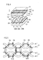
- Fig. 3 is a plan view showing a cell arrangement of a display screen.
- a discharge space 30 is divided into columns by regularly meandering partitions 29, so that column spaces 31 are formed, which has wide portions (portions with large width in the row direction) 31A and narrow portions (portions with small width) 31B arranged alternately.
- each partition 29 is waving at a constant pitch and width in a plan view, and the distance between neighboring partitions 29 becomes smaller than a predetermined value at a constant pitch in the column direction.
- the predetermined value is a size that can suppress discharge and depends on discharge conditions such as gas pressure.
- the structure in which the column space 31 between the neighboring partitions continues over all rows has advantages in easy drive due to priming by column unit, a uniform film thickness of the fluorescent material layer and easy exhaustion process in manufacturing.
- each cell C is a structural body within the area of one wide portion 31A in the display screen.
- a cell is located in every other column.
- the column in which a cell is located is changed in every column.
- cells are located in a zigzag manner both in the row direction and in the column direction.
- Fig. 3 five cells C are shown by dot-dashed circles (a little larger area than real is enclosed for ready viewing in Fig. 3).
- PDP 1 three cells of red, green and blue constitute one pixel, and the three color cells are arranged in triangle (delta) form.
- the triangle arrangement has an advantage for high definition compared with an inline arrangement since the width of the cell is larger than one third of the pixel pitch in the row direction. In addition, since the ratio of non-lighted area to the screen is small, high luminance display can be performed. Furthermore, the horizontal direction is not necessarily the row direction, but the vertical direction can be the row direction while the horizontal direction is the column direction.
- Fig. 4 is a perspective view showing a cell structure of a PDP.
- the display electrodes X and Y, the dielectric layer 17 and the protection film 18 are disposed on the inner surface of the front glass substrate 11, and the address electrodes A, an insulator layer 24, the partition 29 and fluorescent material layers 28R, 28G and 28B are disposed on the inner surface of the back glass substrate 21.
- Each of the display electrodes X and Y includes a transparent conductive film 41 that forms a surface discharge gap and a metal film 42 as a bus conductor.
- the display electrodes X and the display electrodes Y are arranged alternately at a constant pitch (a surface discharge gap) in the column direction.
- the gap direction of the surface discharge gap, i.e., the opposing direction of the display electrodes X and Y is the column direction.
- Fig. 5 is a plan view showing a shape of the display electrode.
- Each of the display electrodes X and Y includes the transparent conductive film 41 extending in the row direction meandering in the column direction and the band-like metal film 42 extending in the row direction meandering along the partition 29 so as to avoid the wide portion 31A.
- the transparent conductive film 41 has a band-like shape curving like a wave and has a arc gap forming portion protruding from the metal film 42 to the wide portion 31A in each column.
- the gap forming portion of the display electrode X and the gap forming portion of the display electrode Y are opposed to each other so as to form a drum-shaped surface discharge gap.
- the opposed sides are not parallel.
- the width of the band-like transparent conductive film 41 can be varied regularly.
- capacitance of the interelectrode distance can be reduced without increasing the surface discharge gap length (i.e., the shortest distance between electrodes).
- the distance between the transparent conductive film 41 and the metal film 42 in the middle of the wide portion 31A in the row direction is large, intensity of electric field generated in the gap between the transparent conductive film 41 and the metal film 42 is small. This contributes to prevention of discharge interference between rows.
- light shield effect of the metal film 42 is relieved, so that the light emission efficiency is increased.
- Fig. 6 shows a concept of frame division.
- each of the sequential frames F that is an input image is divided into a predetermined number q of subframes SF. Namely, each frame F is replaced with a set of q subframes SF.
- weights such as 2 0 , 2 1 , 2 2 , .... 2 q-1 are assigned sequentially so as to set the number of times of display discharge in each subframe SF.
- the subframe arrangement is in the order of weights, but it can be other orders. Redundant weighting can be adopted for reducing false contours.
- the frame period Tf that is a frame transmission period is divided into q subframe periods Tsf, and one subframe period Tsf is assigned to each subframe SF.
- the subframe period Tsf is divided into a reset period TR for initialization, an address period TA for addressing and a display period TS for sustaining.
- the reset period TR and the address period TA have a constant length regardless of the weight, while the display period TS has a variable length that is longer as the weight is larger. Therefore, the length of the subframe period Tsf is also longer as the weight of the corresponding subframe SF is larger.
- the driving sequence is repeated for each subframe, and the order of the reset period TR, the address period TA and the display period TS is the same in q subframes SF.
- a drive waveform in the display period TS that is relevant to the feature of the present invention will be explained.
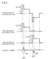
- Fig. 7 is a waveform diagram of the drive voltage signal in the display period.
- Fig. 8 shows the relationship between the drive voltage variation and discharge.
- drive voltage signals concerning two times of display discharge are shown.
- the illustrated drive voltage signals are applied to each electrode repeatedly.
- the drive voltage signal that is applied between electrodes is a combined signal of the drive voltage signals corresponding to the electrodes.
- a drive voltage signal including a sustain pulse Ps and an offset pulse Pos1 is applied to the display electrode X and the display electrode Y, while a drive voltage signal including an offset pulse Pos2 is applied to the address electrode A.
- the sustain pulse Ps is applied to the display electrode X and the display electrode Y alternately, and display discharge is generated in every application. This is because that the amplitude Vs of the sustain pulse Ps is set so that the cell voltage exceeds the discharge start voltage at the XY-interelectrode by applying the sustain pulse Ps even if the amplitude Vos(XY) of the offset pulse Pos1 is zero.
- the offset pulse Pos1 is applied to the other display electrode simultaneously.
- the pulse width Tos(XY) of the offset pulse Pos1 is set to a value substantially smaller than the pulse width of the sustain pulse Ps (approximately a few micro seconds) so that the drive voltages of the XY-interelectrode are different between the start time point ts1 or ts2 and the end time point te1 or te2 of the display discharge as shown in Fig. 8, in other words, so that the application of the offset pulse Posl is finished and the drive voltage changes from Vs + Vos(XY) to Vs during the display discharge.
- the pulse width Tos(XY) is a value within the range of 100-200 ns.
- the offset pulse Pos2 is applied to the address electrode A simultaneously when the sustain pulse Ps is applied to the display electrode X and the display electrode Y.
- the drive voltage at the AY-interelectrode or at the AX-interelectrode (between the address electrode A and the display electrode X) is altered from Vs + Vos(AY) to Vs during display discharge.
- the pulse width Tos(AY) of the offset pulse Pos2 is also substantially shorter than the pulse width of the sustain pulse Ps (The specific value is the same as the offset pulse Pos1).
- Fig. 9 is a cell voltage plan view showing a display process according to the present invention. The explanation here will be performed about the display discharge as a type in which the display electrode X works as an anode and the display electrode Y works as a cathode since the display electrodes X and Y are arranged symmetrically in a cell and the functions of the display electrodes X and Y are the same in the display discharge.
- the cell voltage at the discharge start time point moves along the horizontal axis as shown in Fig. 9.
- the offset pulse Pos2 is added to the sustain pulse Ps
- the cell voltage at the discharge start time point moves along the vertical axis as shown in Fig. 9.
- the application of the offset pulse Pos1 and the offset pulse Pos2 causes two-dimensional movement in the cell voltage plane. This means that the relationship between the cell voltage at the XY-interelectrode and the cell voltage at the AY-interelectrode at the moment of the display discharge generation can be set freely.
- the position showing the cell state of the discharge start time point (indicated by a dot in Fig.
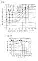
- Fig. 10 is a graph showing dependency of the luminance on the offset voltage.
- Fig. 11 is a graph showing dependency of the light emission efficiency on the offset voltage.
- Vos(XY) the offset voltage Vos(XY)
- Vos(XY) 100 volts
- Vos(XY) 130 volts when the offset voltage Vos(AY) is added.
- the addition of the offset voltage Vos(AY) also contributes to reduction of the withstand voltage of the driving circuit and reduction of the power source voltage.
- the luminance and the light emission efficiency can be improved if the offset voltage Vos(AY) has a value within the range of 50-180 volts as explained above.
- a preferable range of the offset voltage Vos(AY) for being remarkably different to the case where the offset voltage Vos(AY) is zero is 100-180 volts.
- a more preferable range of the offset voltage Vos(AY) is 150-180 volts.
- Concerning the offset voltage Vos(XY) at the XY-interelectrode a preferable range is 80-180 volts for both the luminance and the light emission efficiency to be improved.
- a more preferable range of the offset voltage Vos(XY) is 120-180 volts.
- the drive margin is a difference between the discharge start voltage Vf1 at the XY-interelectrode and the lowest drive voltage Vsmn necessary for maintaining the lighted state.
- the sustain voltage Vs that is amplitude of the sustain pulse Ps is set to a value above Vf1
- discharge may be generated also in the cell that was not lighted in addressing.
- the sustain voltage Vs is set to a value below Vsmn, the lighting cell may go out. Therefore, the sustain voltage Vs is set to a value between Vf1 and Vsmn.
- the offset voltage Vos(XY) is raised, Vsmn drops. Namely, the application of the offset voltage Vos(XY) can lower the sustain voltage Vs, thereby the withstand voltage of the driving circuit can be reduced and the power source voltage can be lowered.
Landscapes
- Engineering & Computer Science (AREA)
- Physics & Mathematics (AREA)
- Power Engineering (AREA)
- Plasma & Fusion (AREA)
- Computer Hardware Design (AREA)
- General Physics & Mathematics (AREA)
- Theoretical Computer Science (AREA)
- Control Of Indicators Other Than Cathode Ray Tubes (AREA)
- Control Of Gas Discharge Display Tubes (AREA)
Abstract
Description
Claims (6)
- A method of driving a plasma display panel having cells in which three or more N electrodes including a pair of display electrodes covered with a dielectric layer are provided, the method comprising:performing addressing for producing wall charge in cells to be lit;altering the potential of at least one display electrode in each of the cells to be lit so as to differ between the start time point and the end time point of display discharge for generating display discharge following reproduction of the wall charge in each of the cells to be lit; andaltering the potential of at least one electrode except the display electrode so as to differ between the start time point and the end time point of the display discharge.
- A method of driving a three-electrode surface discharge AC type plasma display panel having an electrode matrix made of an arrangement of display electrodes and an arrangement of address electrodes, the method comprising:performing addressing for producing wall charge in cells to be lit;altering the potential of at least one display electrode in each of the cells to be lit so as to differ between the start time point and the end time point of display discharge for generating display discharge following reproduction of the wall charge in each of the cells to be lit; andaltering the potential of the address electrode so as to differ between the start time point and the end time point of the display discharge.
- The method according to claim 2, wherein a drive voltage signal is applied between the display electrodes by a potential control in which one of the two display electrodes is temporarily biased and the other display electrode is biased only in the part of the bias period.
- The method according to claim 2 or 3, wherein an applied voltage between the display electrodes at the start time point of the display discharge is set higher than an applied voltage between the display electrodes at the end time point of the display discharge.
- An apparatus for driving a plasma display panel having cells in which three or more N electrodes including a pair of display electrodes covered with a dielectric layer are provided, the apparatus comprising:means for performing addressing for producing wall charge in cells to be lit;means for altering the potential of at least one display electrode in each of the cells to be lit so as to differ between the start time point and the end time point of display discharge for generating display discharge following reproduction of the wall charge in each of the cells to be lit; andmeans for altering the potential of at least one electrode except the display electrode so as to differ between the start time point and the end time point of the display discharge.
- Apparatus for driving a three-electrode surface discharge AC type plasma display panel having an electrode matrix made of an arrangement of display electrodes and an arrangement of address electrodes, the apparatus comprising:means for performing addressing for producing wall charge in cells to be lit;means for altering the potential of at least one display electrode in each of the cells to be lit so as to differ between the start time point and the end time point of display discharge for generating display discharge following reproduction of the wall charge in each of the cells to be lit; andmeans for altering the potential of the address electrode so as to differ between the start time point and the end time point of the display discharge.
Applications Claiming Priority (2)
| Application Number | Priority Date | Filing Date | Title |
|---|---|---|---|
| JP2002036912A JP4158882B2 (en) | 2002-02-14 | 2002-02-14 | Driving method of plasma display panel |
| JP2002036912 | 2002-02-14 |
Publications (2)
| Publication Number | Publication Date |
|---|---|
| EP1336952A2 true EP1336952A2 (en) | 2003-08-20 |
| EP1336952A3 EP1336952A3 (en) | 2007-02-21 |
Family
ID=27621428
Family Applications (1)
| Application Number | Title | Priority Date | Filing Date |
|---|---|---|---|
| EP03250115A Withdrawn EP1336952A3 (en) | 2002-02-14 | 2003-01-09 | Method for driving a plasma display panel improving luminance |
Country Status (4)
| Country | Link |
|---|---|
| US (1) | US6888316B2 (en) |
| EP (1) | EP1336952A3 (en) |
| JP (1) | JP4158882B2 (en) |
| KR (1) | KR20030068388A (en) |
Families Citing this family (11)
| Publication number | Priority date | Publication date | Assignee | Title |
|---|---|---|---|---|
| DE10126930A1 (en) * | 2001-06-01 | 2002-12-05 | Philips Corp Intellectual Pty | Plasma screen with corrugated ribs |
| US7215007B2 (en) * | 2003-06-09 | 2007-05-08 | Wemtec, Inc. | Circuit and method for suppression of electromagnetic coupling and switching noise in multilayer printed circuit boards |
| JP4422443B2 (en) * | 2003-07-22 | 2010-02-24 | パナソニック株式会社 | Display panel drive device |
| CN1324633C (en) * | 2003-09-03 | 2007-07-04 | 友达光电股份有限公司 | AC plasma display panel |
| US7123118B2 (en) * | 2004-03-08 | 2006-10-17 | Wemtec, Inc. | Systems and methods for blocking microwave propagation in parallel plate structures utilizing cluster vias |
| US7157992B2 (en) * | 2004-03-08 | 2007-01-02 | Wemtec, Inc. | Systems and methods for blocking microwave propagation in parallel plate structures |
| KR100615253B1 (en) * | 2004-09-24 | 2006-08-25 | 삼성에스디아이 주식회사 | Driving Method of Plasma Display Panel |
| JP5007021B2 (en) | 2004-12-27 | 2012-08-22 | 株式会社日立製作所 | Plasma display panel driving method and plasma display device |
| JP4713170B2 (en) * | 2005-01-28 | 2011-06-29 | 日立プラズマディスプレイ株式会社 | Plasma display device and driving method thereof |
| KR20060117407A (en) * | 2005-05-10 | 2006-11-17 | 삼성에스디아이 주식회사 | Plasma display panel |
| KR100719035B1 (en) * | 2005-07-01 | 2007-05-16 | 엘지전자 주식회사 | Plasma display panel |
Family Cites Families (12)
| Publication number | Priority date | Publication date | Assignee | Title |
|---|---|---|---|---|
| KR100406781B1 (en) * | 1996-11-08 | 2004-03-24 | 삼성에스디아이 주식회사 | Method for operating discharge device |
| US6020687A (en) * | 1997-03-18 | 2000-02-01 | Fujitsu Limited | Method for driving a plasma display panel |
| JP3028075B2 (en) | 1997-05-30 | 2000-04-04 | 日本電気株式会社 | Driving method of plasma display panel |
| JP3423865B2 (en) * | 1997-09-18 | 2003-07-07 | 富士通株式会社 | Driving method of AC type PDP and plasma display device |
| JP3479900B2 (en) * | 1997-11-13 | 2003-12-15 | 株式会社ティーティーティー | Driving method of AC type PDP |
| JP3421578B2 (en) * | 1998-06-11 | 2003-06-30 | 富士通株式会社 | Driving method of PDP |
| EP1202241B1 (en) * | 1998-09-04 | 2007-09-12 | Matsushita Electric Industrial Co., Ltd. | A plasma display panel driving method and plasma display panel apparatus capable of driving high-quality images with high luminous efficiency |
| JP3556103B2 (en) * | 1998-09-18 | 2004-08-18 | 富士通株式会社 | Driving method of PDP |
| TW554317B (en) * | 2000-11-10 | 2003-09-21 | Au Optronics Corp | Driving method for initial booting period of plasma display panel and its driving circuit |
| JP2002175043A (en) * | 2000-12-06 | 2002-06-21 | Nec Corp | Method for driving plasma display panel, and circuit and display device thereof |
| JP4512971B2 (en) * | 2001-03-02 | 2010-07-28 | 株式会社日立プラズマパテントライセンシング | Display drive device |
| JP3529737B2 (en) * | 2001-03-19 | 2004-05-24 | 富士通株式会社 | Driving method of plasma display panel and display device |
-
2002
- 2002-02-14 JP JP2002036912A patent/JP4158882B2/en not_active Expired - Fee Related
- 2002-12-28 KR KR1020020085830A patent/KR20030068388A/en not_active Ceased
-
2003
- 2003-01-03 US US10/335,864 patent/US6888316B2/en not_active Expired - Fee Related
- 2003-01-09 EP EP03250115A patent/EP1336952A3/en not_active Withdrawn
Also Published As
| Publication number | Publication date |
|---|---|
| JP4158882B2 (en) | 2008-10-01 |
| US20030151373A1 (en) | 2003-08-14 |
| KR20030068388A (en) | 2003-08-21 |
| JP2003241708A (en) | 2003-08-29 |
| US6888316B2 (en) | 2005-05-03 |
| EP1336952A3 (en) | 2007-02-21 |
Similar Documents
| Publication | Publication Date | Title |
|---|---|---|
| US7719487B2 (en) | Method for driving a gas electric discharge device | |
| US8194005B2 (en) | Method of driving plasma display device | |
| US6181305B1 (en) | Method for driving an AC type surface discharge plasma display panel | |
| EP0866439A1 (en) | Method of initialising cells in an AC plasma display panel | |
| US7133005B2 (en) | Plasma display panel and method and apparatus for driving the same | |
| US6888316B2 (en) | Method for driving plasma display panel | |
| JP3532317B2 (en) | Driving method of AC PDP | |
| US7215303B2 (en) | AC-type plasma display panel capable of high definition and high brightness image display, and a method of driving the same | |
| KR20030042435A (en) | AC-type plasma display pannel and method for driving same | |
| KR100721079B1 (en) | Method of driving plasma display panel and plasma display apparatus | |
| US6653793B1 (en) | Plasma display device and method for setting drive operation | |
| EP1471492A2 (en) | Method for driving a plasma display panel | |
| CN100405429C (en) | Plasma display panel driving method and plasma display | |
| KR100484113B1 (en) | Method of driving a plasma display panel | |
| KR100503604B1 (en) | Method of driving plasma display panel | |
| KR20020018893A (en) | Method for driving a plasma diplay panel | |
| KR100453161B1 (en) | Plasma Display Panel and Driving Method Thereof and Fabricating Method of lower Plate Thereof | |
| KR100775204B1 (en) | Method for driving plasma display panel and plasma display device | |
| KR100515339B1 (en) | A plasma display panel and a driving method thereof | |
| JPH09311663A (en) | Driving method of plasma display panel | |
| KR20060119394A (en) | Driving Method of Plasma Display Panel Using Auxiliary Pulse with Phase Difference | |
| KR20040077078A (en) | Method for reducing address period in ac plasma display panel | |
| KR20080037102A (en) | Driving method and display device of plasma display panel | |
| JP2005010424A (en) | Driving method of plasma display panel | |
| KR20050014588A (en) | Method for driving plasma display panel during sustain period |
Legal Events
| Date | Code | Title | Description |
|---|---|---|---|
| PUAI | Public reference made under article 153(3) epc to a published international application that has entered the european phase |
Free format text: ORIGINAL CODE: 0009012 |
|
| AK | Designated contracting states |
Designated state(s): AT BE BG CH CY CZ DE DK EE ES FI FR GB GR HU IE IT LI LU MC NL PT SE SI SK TR |
|
| AX | Request for extension of the european patent |
Extension state: AL LT LV MK RO |
|
| RAP1 | Party data changed (applicant data changed or rights of an application transferred) |
Owner name: HITACHI, LTD. |
|
| PUAL | Search report despatched |
Free format text: ORIGINAL CODE: 0009013 |
|
| AK | Designated contracting states |
Kind code of ref document: A3 Designated state(s): AT BE BG CH CY CZ DE DK EE ES FI FR GB GR HU IE IT LI LU MC NL PT SE SI SK TR |
|
| AX | Request for extension of the european patent |
Extension state: AL LT LV MK RO |
|
| RAP1 | Party data changed (applicant data changed or rights of an application transferred) |
Owner name: HITACHI PLASMA PATENT LICENSING CO., LTD. |
|
| 17P | Request for examination filed |
Effective date: 20070816 |
|
| AKX | Designation fees paid |
Designated state(s): DE FR GB |
|
| 17Q | First examination report despatched |
Effective date: 20071001 |
|
| STAA | Information on the status of an ep patent application or granted ep patent |
Free format text: STATUS: THE APPLICATION IS DEEMED TO BE WITHDRAWN |
|
| 18D | Application deemed to be withdrawn |
Effective date: 20100803 |