JP4422443B2 - Display panel drive device - Google Patents
Display panel drive device Download PDFInfo
- Publication number
- JP4422443B2 JP4422443B2 JP2003199660A JP2003199660A JP4422443B2 JP 4422443 B2 JP4422443 B2 JP 4422443B2 JP 2003199660 A JP2003199660 A JP 2003199660A JP 2003199660 A JP2003199660 A JP 2003199660A JP 4422443 B2 JP4422443 B2 JP 4422443B2
- Authority
- JP
- Japan
- Prior art keywords
- voltage
- pulse
- sustain
- discharge
- row electrode
- Prior art date
- Legal status (The legal status is an assumption and is not a legal conclusion. Google has not performed a legal analysis and makes no representation as to the accuracy of the status listed.)
- Expired - Fee Related
Links
Images


Classifications
-
- G—PHYSICS
- G09—EDUCATION; CRYPTOGRAPHY; DISPLAY; ADVERTISING; SEALS
- G09G—ARRANGEMENTS OR CIRCUITS FOR CONTROL OF INDICATING DEVICES USING STATIC MEANS TO PRESENT VARIABLE INFORMATION
- G09G3/00—Control arrangements or circuits, of interest only in connection with visual indicators other than cathode-ray tubes
- G09G3/20—Control arrangements or circuits, of interest only in connection with visual indicators other than cathode-ray tubes for presentation of an assembly of a number of characters, e.g. a page, by composing the assembly by combination of individual elements arranged in a matrix no fixed position being assigned to or needed to be assigned to the individual characters or partial characters
- G09G3/2007—Display of intermediate tones
- G09G3/2018—Display of intermediate tones by time modulation using two or more time intervals
- G09G3/2022—Display of intermediate tones by time modulation using two or more time intervals using sub-frames
- G09G3/2029—Display of intermediate tones by time modulation using two or more time intervals using sub-frames the sub-frames having non-binary weights
-
- G—PHYSICS
- G09—EDUCATION; CRYPTOGRAPHY; DISPLAY; ADVERTISING; SEALS
- G09G—ARRANGEMENTS OR CIRCUITS FOR CONTROL OF INDICATING DEVICES USING STATIC MEANS TO PRESENT VARIABLE INFORMATION
- G09G3/00—Control arrangements or circuits, of interest only in connection with visual indicators other than cathode-ray tubes
- G09G3/20—Control arrangements or circuits, of interest only in connection with visual indicators other than cathode-ray tubes for presentation of an assembly of a number of characters, e.g. a page, by composing the assembly by combination of individual elements arranged in a matrix no fixed position being assigned to or needed to be assigned to the individual characters or partial characters
- G09G3/22—Control arrangements or circuits, of interest only in connection with visual indicators other than cathode-ray tubes for presentation of an assembly of a number of characters, e.g. a page, by composing the assembly by combination of individual elements arranged in a matrix no fixed position being assigned to or needed to be assigned to the individual characters or partial characters using controlled light sources
- G09G3/28—Control arrangements or circuits, of interest only in connection with visual indicators other than cathode-ray tubes for presentation of an assembly of a number of characters, e.g. a page, by composing the assembly by combination of individual elements arranged in a matrix no fixed position being assigned to or needed to be assigned to the individual characters or partial characters using controlled light sources using luminous gas-discharge panels, e.g. plasma panels
- G09G3/288—Control arrangements or circuits, of interest only in connection with visual indicators other than cathode-ray tubes for presentation of an assembly of a number of characters, e.g. a page, by composing the assembly by combination of individual elements arranged in a matrix no fixed position being assigned to or needed to be assigned to the individual characters or partial characters using controlled light sources using luminous gas-discharge panels, e.g. plasma panels using AC panels
- G09G3/291—Control arrangements or circuits, of interest only in connection with visual indicators other than cathode-ray tubes for presentation of an assembly of a number of characters, e.g. a page, by composing the assembly by combination of individual elements arranged in a matrix no fixed position being assigned to or needed to be assigned to the individual characters or partial characters using controlled light sources using luminous gas-discharge panels, e.g. plasma panels using AC panels controlling the gas discharge to control a cell condition, e.g. by means of specific pulse shapes
- G09G3/293—Control arrangements or circuits, of interest only in connection with visual indicators other than cathode-ray tubes for presentation of an assembly of a number of characters, e.g. a page, by composing the assembly by combination of individual elements arranged in a matrix no fixed position being assigned to or needed to be assigned to the individual characters or partial characters using controlled light sources using luminous gas-discharge panels, e.g. plasma panels using AC panels controlling the gas discharge to control a cell condition, e.g. by means of specific pulse shapes for address discharge
- G09G3/2937—Control arrangements or circuits, of interest only in connection with visual indicators other than cathode-ray tubes for presentation of an assembly of a number of characters, e.g. a page, by composing the assembly by combination of individual elements arranged in a matrix no fixed position being assigned to or needed to be assigned to the individual characters or partial characters using controlled light sources using luminous gas-discharge panels, e.g. plasma panels using AC panels controlling the gas discharge to control a cell condition, e.g. by means of specific pulse shapes for address discharge being addressed only once per frame
-
- G—PHYSICS
- G09—EDUCATION; CRYPTOGRAPHY; DISPLAY; ADVERTISING; SEALS
- G09G—ARRANGEMENTS OR CIRCUITS FOR CONTROL OF INDICATING DEVICES USING STATIC MEANS TO PRESENT VARIABLE INFORMATION
- G09G2310/00—Command of the display device
- G09G2310/06—Details of flat display driving waveforms
- G09G2310/066—Waveforms comprising a gently increasing or decreasing portion, e.g. ramp
-
- G—PHYSICS
- G09—EDUCATION; CRYPTOGRAPHY; DISPLAY; ADVERTISING; SEALS
- G09G—ARRANGEMENTS OR CIRCUITS FOR CONTROL OF INDICATING DEVICES USING STATIC MEANS TO PRESENT VARIABLE INFORMATION
- G09G3/00—Control arrangements or circuits, of interest only in connection with visual indicators other than cathode-ray tubes
- G09G3/20—Control arrangements or circuits, of interest only in connection with visual indicators other than cathode-ray tubes for presentation of an assembly of a number of characters, e.g. a page, by composing the assembly by combination of individual elements arranged in a matrix no fixed position being assigned to or needed to be assigned to the individual characters or partial characters
- G09G3/22—Control arrangements or circuits, of interest only in connection with visual indicators other than cathode-ray tubes for presentation of an assembly of a number of characters, e.g. a page, by composing the assembly by combination of individual elements arranged in a matrix no fixed position being assigned to or needed to be assigned to the individual characters or partial characters using controlled light sources
- G09G3/28—Control arrangements or circuits, of interest only in connection with visual indicators other than cathode-ray tubes for presentation of an assembly of a number of characters, e.g. a page, by composing the assembly by combination of individual elements arranged in a matrix no fixed position being assigned to or needed to be assigned to the individual characters or partial characters using controlled light sources using luminous gas-discharge panels, e.g. plasma panels
- G09G3/288—Control arrangements or circuits, of interest only in connection with visual indicators other than cathode-ray tubes for presentation of an assembly of a number of characters, e.g. a page, by composing the assembly by combination of individual elements arranged in a matrix no fixed position being assigned to or needed to be assigned to the individual characters or partial characters using controlled light sources using luminous gas-discharge panels, e.g. plasma panels using AC panels
- G09G3/291—Control arrangements or circuits, of interest only in connection with visual indicators other than cathode-ray tubes for presentation of an assembly of a number of characters, e.g. a page, by composing the assembly by combination of individual elements arranged in a matrix no fixed position being assigned to or needed to be assigned to the individual characters or partial characters using controlled light sources using luminous gas-discharge panels, e.g. plasma panels using AC panels controlling the gas discharge to control a cell condition, e.g. by means of specific pulse shapes
- G09G3/293—Control arrangements or circuits, of interest only in connection with visual indicators other than cathode-ray tubes for presentation of an assembly of a number of characters, e.g. a page, by composing the assembly by combination of individual elements arranged in a matrix no fixed position being assigned to or needed to be assigned to the individual characters or partial characters using controlled light sources using luminous gas-discharge panels, e.g. plasma panels using AC panels controlling the gas discharge to control a cell condition, e.g. by means of specific pulse shapes for address discharge
- G09G3/2935—Addressed by erasing selected cells that are in an ON state
-
- G—PHYSICS
- G09—EDUCATION; CRYPTOGRAPHY; DISPLAY; ADVERTISING; SEALS
- G09G—ARRANGEMENTS OR CIRCUITS FOR CONTROL OF INDICATING DEVICES USING STATIC MEANS TO PRESENT VARIABLE INFORMATION
- G09G3/00—Control arrangements or circuits, of interest only in connection with visual indicators other than cathode-ray tubes
- G09G3/20—Control arrangements or circuits, of interest only in connection with visual indicators other than cathode-ray tubes for presentation of an assembly of a number of characters, e.g. a page, by composing the assembly by combination of individual elements arranged in a matrix no fixed position being assigned to or needed to be assigned to the individual characters or partial characters
- G09G3/22—Control arrangements or circuits, of interest only in connection with visual indicators other than cathode-ray tubes for presentation of an assembly of a number of characters, e.g. a page, by composing the assembly by combination of individual elements arranged in a matrix no fixed position being assigned to or needed to be assigned to the individual characters or partial characters using controlled light sources
- G09G3/28—Control arrangements or circuits, of interest only in connection with visual indicators other than cathode-ray tubes for presentation of an assembly of a number of characters, e.g. a page, by composing the assembly by combination of individual elements arranged in a matrix no fixed position being assigned to or needed to be assigned to the individual characters or partial characters using controlled light sources using luminous gas-discharge panels, e.g. plasma panels
- G09G3/288—Control arrangements or circuits, of interest only in connection with visual indicators other than cathode-ray tubes for presentation of an assembly of a number of characters, e.g. a page, by composing the assembly by combination of individual elements arranged in a matrix no fixed position being assigned to or needed to be assigned to the individual characters or partial characters using controlled light sources using luminous gas-discharge panels, e.g. plasma panels using AC panels
- G09G3/296—Driving circuits for producing the waveforms applied to the driving electrodes
- G09G3/2965—Driving circuits for producing the waveforms applied to the driving electrodes using inductors for energy recovery
Description
【0001】
【発明が属する技術分野】
本発明は、容量性の放電セルを備えた表示パネルの駆動装置に関する。
【0002】
【従来の技術】
現在、薄型の表示デバイスとして交流放電型のプラズマディスプレイパネルを搭載したプラズマディスプレイ装置が知られている。
交流放電型のプラズマディスプレイパネル(以下、PDPと称する)は、複数の列電極と、放電ガスが封入されている放電空間を挟んで上記列電極各々と交叉して配列された複数の行電極対を備えている。そして、この放電空間を含む各行電極対と列電極との各交差部に、その放電時において赤色で発光する放電セル、緑色で発光する放電セル、又は青色で発光する放電セルが形成されている。
【0003】
この際、各放電セルは、放電現象を利用して発光を行うものである為、所定の輝度で発光する「点灯状態」と、「消灯状態」の2つの状態しかもたない。つまり、2階調分の輝度しか表現出来ないのである。そこで、このような放電セルを用いて、入力された映像信号に対応した中間調の輝度表示を実現させるべく、サブフィールド法を用いた階調駆動を実施する(例えば、特許文献1参照)。
【0004】
サブフィールド法では、1フィールドの表示期間をN個のサブフィールドに分割し、各サブフィールドに、放電セルを連続して発光(又は消灯)させるべき期間を予め割り付けておく。そして、各サブフィールド毎に放電セル各々をそのサブフィールドに割り当てられている期間だけ、入力映像信号に応じて発光、又は消灯させるのである。これにより、1フィールド表示期間内において発光を実施させるサブフィールドの組み合わせにより、2N(N:サブフィールドの数)段階(以下、階調と称する)で各種の中間輝度を表現することが可能となる。
【0005】
ここで、上記サブフィールド法に基づく階調駆動を実施するにあたり、駆動装置(図示せぬ)は、PDPに対して各種駆動パルスを印加することにより、放電セルの各々に種々の放電を生起させる。すなわち、先ず、駆動装置は、PDPの行電極対にリセットパルスを印加することにより、全ての放電セルにリセット放電を生起させる。この際、上記リセット放電により、所定量の壁電荷が全放電セル内に一様に形成される。次に、駆動装置は、放電セルを1水平走査ライン(以下、1表示ラインと称する)分ずつ順次、入力映像信号に応じて選択的に消去放電させる。この際、選択消去放電の生起された放電セルではその放電セル内に残留していた壁電荷が消滅する。一方、上記選択消去放電の生起されなかった放電セルでは、上記リセット放電によって形成された壁電荷がそのまま残留することになる。次に、駆動装置は、全ての行電極対間に交互に、かつ一斉に各サブフィールドに対応した回数だけ維持パルスを印加する。かかる維持パルスの印加に応じて、壁電荷が残留している放電セルのみがサブフィールドに対応した期間だけ繰り返し維持放電し、この維持放電に伴う発光の状態を維持する。
【0006】
ところが、PDPでは、パネルの温度変動、表示輝度の推移、経年変化等によって、上述した如き各種放電によって形成される壁電荷の量が一定とはならなくなる為、放電の強度にバラツキが生じて表示品質が劣化するという問題があった。
【0007】
【特許文献1】
特開2000−338932号公報
【0008】
【発明が解決しようとする課題】
本発明は、上記の問題を解決するためになされたものであり、常時、良好な画像表示を行うことが出来る表示パネルの駆動装置を提供することを目的とする。
【0009】
【課題を解決するための手段】
請求項1記載による表示パネルの駆動装置は、表示ラインに対応した複数の行電極と前記行電極各々に交叉して配列された複数の列電極とを有し前記行電極及び前記列電極の各交差部に画素を担う容量性の放電セルが形成されている表示パネルを、入力映像信号の各フィールドを構成する複数のサブフィールド毎に駆動する表示パネルの駆動装置であって、前記サブフィールド各々において前記行電極に走査パルスを印加すると共に前記入力映像信号に対応した画素データパルスを前記列電極に印加することにより前記放電セルの各々を選択的に放電せしめて前記放電セルを点灯モード又は消灯モードのいずれか一方に設定するアドレス手段と、前記サブフィールド各々において前記行電極に繰り返し維持パルスを印加することにより前記点灯モードにある前記放電セルのみを繰り返し維持放電せしめる発光維持手段と、を有し、前記サブフィールド内において前記行電極に印加される前記維持パルス各々の内の最終の維持パルスのみ、その電圧値の立ち下がり区間が、前記電圧値が前記最終の維持パルスの直前に印加される維持パルスの立ち下がり区間での電圧低下よりも緩やかに低下する第1電圧低下区間と、前記第1電圧低下区間に後続して前記電圧値が所定期間に亘り一定となる電圧一定区間と、前記電圧一定区間に後続して前記第1電圧低下区間におけるよりも緩やかに電圧値が低下する第2電圧低下区間と、を有する。
【0010】
【発明の実施の形態】
以下、本発明の実施例を図面を参照しつつ詳細に説明する。
図1は、表示パネルとしてプラズマディスプレイパネルを搭載したプラズマディスプレイ装置の概略構成を示す図である。
図1において、プラズマディスプレイパネルとしてのPDP10は、m個の列電極D1〜Dmと、これら列電極各々と交叉して配列された夫々n個の行電極X1〜Xn及び行電極Y1〜Ynを備えている。これら行電極X1〜Xn及び行電極Y1〜Ynは、夫々一対の行電極Xi(1≦i≦n)及びYi(1≦i≦n)にて、PDP10における第1表示ライン〜第n表示ラインを担っている。列電極Dと、行電極X及びYとの間には、放電ガスが封入されている放電空間が形成されている。そして、この放電空間を含む各行電極対と列電極との各交差部に、容量性の放電セルが形成される構造となっている。
【0011】
A/D変換器1は、駆動制御回路2から供給されたクロック信号に応じてアナログの入力映像信号をサンプリングし、これを各画素に対応した例えば4ビットの画素データPDに変換する。画素駆動データ生成回路30は、4ビットの画素データPDを、図2に示す如きデータ変換テーブルに従って14ビットの画素駆動データGDに変換し、これをメモリ4に供給する。メモリ4は、4ビットの画素駆動データGDを順次取り込んで記憶する。そして、1画像フレーム(n行×m列)分の画素駆動データGD1,1〜GDn,mの書き込みが終了する度に、メモリ4は、画素駆動データGD1,1〜GDn,m各々を各ビット桁(第1〜第14ビット)毎に分離し、夫々、後述するサブフィールドSF1〜SF14に対応させて1表示ライン分ずつ読み出す。メモリ4は、読み出した1表示ライン分(m個)の画素駆動データビットを画素駆動データビットDB1〜DB(m)としアドレスドライバ6に供給する。
【0012】
駆動制御回路2は、上記入力映像信号中の水平及び垂直同期信号に同期して、上記A/D変換器1に対するクロック信号、及びメモリ4に対する書込・読出信号を発生する。更に、駆動制御回路2は、かかる水平及び垂直同期信号に同期して、アドレスドライバ6、第1サスティンドライバ7及び第2サスティンドライバ8各々を駆動制御すべき各種タイミング信号を発生する。
【0013】
アドレスドライバ6は、メモリ4から読み出された1表示ライン分毎の画素駆動データビットDB各々の論理レベルに対応した電圧を有するm個の画素データパルスの各々を列電極D1〜Dmに夫々印加する。第1サスティンドライバ7及び第2サスティンドライバ8は、PDP10の放電セル各々に各種の放電を生起させるべき各種駆動パルスを発生して、PDP10の行電極X1〜Xn及びY1〜Ynに印加する。駆動制御回路2は、図3に示す如き発光駆動フォーマットに従ってPDP10を階調駆動すべく、各種スイッチング信号SW(後述する)を、アドレスドライバ6、第1サスティンドライバ7及び第2サスティンドライバ8各々に供給する。
【0014】
尚、図3に示される発光駆動フォーマットでは、1フィールドの表示期間を14個のサブフィールドSF1〜SF14に分割し、各サブフィールドにおいてPDP10を駆動する。この際、各サブフィールド内ではアドレス行程Wc及び発光維持行程Icを実施し、先頭のサブフィールドSF1内においてのみで一斉リセット行程Rcを実行する。又、最後尾のサブフィールドSF14においてのみで消去行程Eを実施する。
【0015】
図4は、上記一斉リセット行程Rc、アドレス行程Wc、発光維持行程Ic及び消去行程Eにおいて上記アドレスドライバ6、第1サスティンドライバ7及び第2サスティンドライバ8各々がPDP10に印加する各種駆動パルスと、その印加タイミングを示す図である。
先ず、先頭のサブフィールドSF1において実施される一斉リセット行程Rcでは、第1サスティンドライバ7及び第2サスティンドライバ8各々が、PDP10の行電極X1〜Xn及びY1〜Yn各々に対して図4に示す如き波形を有する第1リセットパルスRPx1及びRPY1を同時に印加する。これにより、PDP10中の全ての放電セルがリセット放電されて、各放電セル内には一様に所定量の壁電荷が形成される。そして、上記第1リセットパルスRPx1及びRPY1の印加直後、第1サスティンドライバ7は、図4に示す如き第2リセットパルスRP2を行電極X1〜Xnの各々に同時印加する。更に、この第2リセットパルスRP2の印加直後、第2サスティンドライバ8は、図4に示す如き第3リセットパルスRP3を行電極Y1〜Ynの各々に同時印加する。この際、上記第2リセットパルスRP2及び第3リセットパルスRP3が印加される度に、各放電セルにリセット放電が生起され、その放電空間内には所望量のプライミング粒子が形成される。かかる一斉リセット行程Rcにより、全ての放電セル内には一様に壁電荷が形成され、全放電セルが点灯モードに初期化される。
【0016】
次に、アドレス行程Wcでは、アドレスドライバ6は、メモリ4から供給された1表示ライン分の画素駆動データビットDB1〜DB(m)各々の論理レベルに応じたm個の画素データパルスを生成し、これらm個の画素データパルスからなる画素データパルス群DPを列電極D1〜Dmに印加する。
例えば、アドレスドライバ6は、サブフィールドSF1のアドレス行程Wcでは、先ず、第1表示ラインに対応した画素駆動データビットDB1〜DB(m)各々に基づくm個の画素データパルスからなる画素データパルス群DP1を列電極D1〜Dmに印加する。次に、アドレスドライバ6は、第2表示ラインに対応した画素駆動データビットDB1〜DB(m)各々に対応したm個の画素データパルスからなる画素データパルス群DP2を列電極D1〜Dmに印加する。以降、アドレスドライバ6は、第3表示ライン〜第n表示ライン各々に対応した画素データパルス群DP3〜DP(n)を図4に示す如く順次、列電極D1〜Dmに印加して行く。尚、アドレスドライバ6は、画素駆動データビットDBが論理レベル0である場合には低電圧(0ボルト)、論理レベル1である場合には高電圧の画素データパルスを生成する。
【0017】
更に、上記アドレス行程Wcでは、第2サスティンドライバ8が、各画素データパルス群DPの印加タイミングと同一タイミングにて、図4に示されるが如き走査パルスSPを発生してこれを行電極Y1〜Ynへと順次印加して行く。この際、走査パルスSPが印加された行電極と、高電圧の画素データパルスが印加された列電極との交差部の放電セルにのみ選択的に放電(選択消去放電)が生じ、その放電セル内に残存していた壁電荷が消去される。ここで、上記選択消去放電が生起されて壁電荷を失った放電セルは消灯モードに遷移する。一方、上記選択消去放電の生起されなかった放電セル内には壁電荷が残留したままとなるので、この放電セルは点灯モードの状態を維持する。
【0018】
すなわち、アドレス行程Wcの実行により、画素データに応じて各放電セルが点灯モード又は消灯モードのいずれか一方に設定される、いわゆる画素データの書き込みが為されるのである。
次に、サブフィールドSF1〜SF14各々の発光維持行程Icでは、第1サスティンドライバ7及び第2サスティンドライバ8が行電極X1〜Xn及びY1〜Ynに対して図4に示されるように交互に維持パルスIPX及びIPYを繰り返し印加する。尚、かかる発光維持行程Icにおいて印加する維持パルスIPの回数は、図3に示されるように各サブフィールド毎に異なる。
【0019】
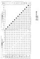
すなわち、サブフィールドSF1の発光維持行程Icでの維持パルスIPの印加回数を「1」とした場合、
SF1:1
SF2:3
SF3:5
SF4:8
SF5:10
SF6:13
SF7:16
SF8:19
SF9:22
SF10:25
SF11:28
SF12:32
SF13:35
SF14:39
なる回数比となるように、各サブフィールドの発光維持行程Icでの維持パルスIPの印加回数が設定されている。
【0020】
この際、壁電荷が残留したままとなっている放電セル、すなわち上記アドレス行程Wcにおいて点灯モードに設定された放電セルのみが、上記維持パルスIPX及びIPYが印加される度に維持放電し、各サブフィールド毎に割り当てられた放電回数分だけ、その維持放電に伴う発光状態を維持する。尚、各発光維持行程Ic内において最後に生起される維持放電は、次のサブフィールドのアドレス行程Wcでの選択消去放電を適切に生起させるべく、各放電セル内に残留する壁電荷の量を適量に調整する役目をも担っている。
【0021】
ここで、各放電セルがアドレス行程Wcにおいて点灯モード又は消灯モードのいずれに設定されるのかは、入力映像信号に基づいて生成された上記画素駆動データGDによって決まる。この際、14ビットの画素駆動データGDとして取り得るパターンは、図2に示されるが如き15パターンである。図2に示す如き15パターン分の画素駆動データGDは、その第1ビット〜第14ビット各々の内で論理レベル1となるビットが必ず1つ以下となる。従って、かかる画素駆動データGDを用いた駆動によれば、図2の黒丸印にて示すように、サブフィールドSF1〜SF14の内の1つのサブフィールドでのアドレス行程Wcにおいてのみで選択消去放電が生起される。すなわち、一斉リセット行程RcによってPDP10の全放電セル内に形成された壁電荷は、上記選択消去放電が生起されるまで残留する。つまり、各放電セルは1フィールド期間内において上記選択消去放電が為されるまでの間、点灯モードの状態を保持し、その間に存在するサブフィールド各々の発光維持行程Ic(白丸にて示す)において連続して維持放電発光するのである。
【0022】
そして、最後尾のサブフィールドSF14のみで実施される消去行程Eでは、アドレスドライバ6が、消去パルスAPを発生してこれを列電極D1-mの各々に印加する。更に、第2サスティンドライバ8は、かかる消去パルスAPの印加タイミングと同時に消去パルスEPを発生してこれを行電極Y1〜Yn各々に印加する。これら消去パルスAP及びEPの同時印加により、PDP10における全放電セル内において消去放電が生起され、全ての放電セル内に残存している壁電荷が消滅する。
【0023】
従って、図2に示す如き15パターンからなる画素駆動データGDを用いて図3に示す発光駆動フォーマットに従った駆動を実施すれば、
{0、1、4、9、17、27、40、56、75、97、122、150、182、217、255}
なる15段階分の中間輝度が表現可能となり、PDP10の画面上には入力映像信号に対応した表示画像が表れることになる。
【0024】
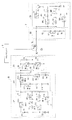
図5は、上記リセットパルスRP、走査パルスSP、維持パルスIP及び消去パルスEPを発生する第1サスティンドライバ7及び第2サスティンドライバ8各々の内部構成を示す図である。
図5に示すように、第1サスティンドライバ7には、上記リセットパルスRPXを発生するリセットパルス発生回路RX、及び上記維持パルスIPXを発生する維持パルス発生回路IXが設けられている。
【0025】
リセットパルス発生回路RXは、直流の電圧VRを発生する直流電源B2、スイッチング素子S7、及び抵抗R1から構成される。直流電源B2の正極端子はアース電位に設定されており、その負極端子は上記スイッチング素子S7に接続されている。スイッチング素子S7は、駆動制御回路2から供給されたスイッチング信号SW7が論理レベル1である期間中に限りオン状態となり、直流電源B2の負極端子の電圧(−VR)を抵抗R1を介して行電極Xに印加する。
【0026】
維持パルス発生回路IXは、直流の電圧VSを発生する直流電源B1、スイッチング素子S1〜S4、コイルL1及びL2、ダイオードD1及びD2、及びコンデンサC1から構成される。スイッチング素子S1は、駆動制御回路2から供給されたスイッチング信号SW1が論理レベル1である期間中に限りオン状態となり、コンデンサC1の一方の電極端子の電圧をコイルL1、ダイオードD1を介して行電極Xに印加する。スイッチング素子S2は、駆動制御回路2から供給されたスイッチング信号SW2が論理レベル1である期間中に限りオン状態となり、行電極X上の電圧をコイルL2、及びダイオードD2を介してコンデンサC1の一方の電極端子に印加する。スイッチング素子S3は、駆動制御回路2から供給されたスイッチング信号SW3が論理レベル1である期間中に限りオン状態となり、上記直流電源B1が発生した電圧VSを行電極Xに印加する。スイッチング素子S4は、駆動制御回路2から供給されたスイッチング信号SW4が論理レベル1である期間中に限りオン状態となり、行電極Xをアース電位に設定する。
【0027】
一方、第2サスティンドライバ8には、図5に示す如きリセットパルスRPYを発生するリセットパルス発生回路RY、上記走査パルスSPを発生する走査パルス発生回路SY、及び上記維持パルスIPY及びIPYEを発生する維持パルス発生回路IYが設けられている。
リセットパルス発生回路RYは、直流の電圧VRを発生する直流電源B4、スイッチング素子S15〜S17、ダイオードD10、抵抗R2及びR3から構成される。直流電源B4の負極端子は接地されており、その正極端子は上記スイッチング素子S17に接続されている。スイッチング素子S17は、駆動制御回路2から供給されたスイッチング信号SW17が論理レベル1である期間中に限りオン状態となり、直流電源B4の正極端子の電圧VRを抵抗R3を介してライン20上に印加する。ダイオードD10は、そのカソード電極がアース電位に設定されている。抵抗R2の一方の電極端子にはダイオードD10のアノード電極が接続されており、その他方の電極端子にはスイッチング素子S16が接続されている。スイッチング素子S16は、駆動制御回路2から供給されたスイッチング信号SW16が論理レベル1である期間中に限りオン状態となり、抵抗R2の他方の電極端子とライン12とを接続する。
【0028】
維持パルス発生回路IYは、直流の電圧VSを発生する直流電源B3、スイッチング素子S11〜S14、コイルL3及びL4、ダイオードD3及びD4、及びコンデンサC2から構成される。スイッチング素子S11は、駆動制御回路2から供給されたスイッチング信号SW11が論理レベル1である期間中に限りオン状態となり、コンデンサC2の一方の電極端子上の電圧をコイルL3、ダイオードD3を介してライン12上に印加する。スイッチング素子S12は、駆動制御回路2から供給されたスイッチング信号SW12が論理レベル1である期間中に限りオン状態となり、上記ライン12上の電圧をコイルL4、及びダイオードD4を介してコンデンサC2の一方の電極端子に印加する。スイッチング素子S13は、駆動制御回路2から供給されたスイッチング信号SW13が論理レベル1である期間中に限りオン状態となり、上記直流電源B3が発生した電圧VSを上記ライン12上に印加する。スイッチング素子S14は、駆動制御回路2から供給されたスイッチング信号SW14が論理レベル1である期間中に限りオン状態となり、上記ライン12をアース電位に設定する。
【0029】
走査パルス発生回路SYは、行電極Y1〜Yn毎に設けられており、夫々、直流の電圧Vhを発生する直流電源B5、スイッチング素子S21、S22、ダイオードD5及びD6から構成される。スイッチング素子S21は、駆動制御回路2から供給されたスイッチング信号SW21が論理レベル1である期間中に限りオン状態となり、直流電源B5の正極端子と、ダイオードD5のアノード電極を行電極Yに夫々接続する。スイッチング素子S22は、駆動制御回路2から供給されたスイッチング信号SW22が論理レベル1である期間中に限りオン状態となり、直流電源B5の負極端子と、ダイオードD6のカソード電極を行電極Yに夫々接続する。駆動制御回路2は、図4に示す如きアドレス行程Wcにおいて、論理レベル0のスイッチング信号SW21及び論理レベル1のスイッチング信号SW22を、行電極Y1〜Yn毎に設けられた走査パルス発生回路SYの各々に対して順次印加する。これにより、直流電源B5の負極端子側の電圧(−Vh)に基づく図4に示す如き負極性の走査パルスSPが順次、行電極Y1〜Ynへと印加されて行く。
【0030】
次に、図5に示される構成による第1リセットパルスRPX1、RPY1、第2リセットパルスRP2、及び第3リセットパルスRP3各々の生成動作について、図6を参照しつつ説明する。
図6において、先ず、駆動制御回路2は、論理レベル1のスイッチング信号SW7をスイッチング素子S7に供給する。この際、スイッチング素子S7はオン状態となり、直流電源B2の負極端子の電圧(−VR)が抵抗R1を介して行電極Xに印加される。これにより、PDP10の負荷容量C0が充電され、行電極X上の電圧は図6に示す如く0ボルトの状態から徐々に低下する。そして、所定期間経過後に、駆動制御回路2は、論理レベル1のスイッチング信号SW4をスイッチング素子S4に供給する。スイッチング素子S4は、論理レベル1のスイッチング信号SW4に応じてオン状態となり、行電極Xをアース電位に設定する。よって、図6に示す如く行電極X上の電圧は急峻に0ボルトに遷移する。
【0031】
よって、上記の如き一連の動作により、その立ち下がりが緩やかであり且つ立ち上がりが急峻な波形を有する図6に示す如き負極性の第1リセットパルスRPx1が生成される。
又、この間、駆動制御回路2は、論理レベル0のスイッチング信号SW15をスイッチング素子S15に供給すると共に、論理レベル1のスイッチング信号SW17をスイッチング素子S17、論理レベル1のスイッチング信号SW21をスイッチング素子S22に夫々供給する。この際、スイッチング素子S17及び21が共にオン状態となり、直流電源B4の正極端子の電圧VRがスイッチング素子S17、抵抗R3、ライン20、及びスイッチング素子S21を介して行電極Yに印加される。これにより、PDP10の負荷容量C0が充電され、行電極Y上の電圧は図6に示す如く0ボルトの状態から徐々に上昇する。そして、所定期間経過後に、前述した如くスイッチング素子S4がオン状態となるので、図6に示す如く行電極Y上の電圧は急峻に0ボルトに遷移する。
【0032】
上記の如き一連の動作により、図6に示す如く、その立ち上がりが緩やかであり且つ立ち下がりが急峻な波形を有するき正極性の第1リセットパルスRPY1が生成される。
次に、駆動制御回路2は、図6に示す如きスイッチングシーケンスSRXに従って状態が推移するスイッチング信号SW1〜SW4を、維持パルス発生回路IXのスイッチング素子S1〜S4に夫々供給する。かかるスイッチングシーケンスSRXによれば、先ず、スイッチング素子S1のみがオン状態となり、コンデンサC1に蓄えられていた電荷に伴う電流がコイルL1、ダイオードD1、行電極Xを介して放電セルに流れ込む。これにより、行電極X上の電圧は図6に示す如く徐々に上昇して行く。次に、スイッチング素子S3のみがオン状態となり、直流電源B1の正極端子の電圧VSが直に行電極Xに印加される。これにより、行電極X上の電圧は図6に示す如く電圧VSとなる。次に、スイッチング素子S2のみがオン状態となり、行電極X及びY間の負荷容量C0に蓄えられていた電荷に伴う電流がコイルL2、ダイオードD2を介してコンデンサC1に流れ込む。これにより、行電極X上の電圧は図6に示す如く徐々に低下して行く。
【0033】
よって、スイッチングシーケンスSRXによれば、図6に示す如く、その立ち上がり及び立ち下がりが共に緩やかな波形を有する正極性の第2リセットパルスRP2が生成される。
この際、かかる第2リセットパルスRP2に応じて行電極X上の電圧が0ボルトから電圧VSに推移するとリセット放電が生起され、更に、行電極X上の電圧が電圧VSから0ボルトに推移する区間、つまり第2リセットパルスRP2の立ち下がり区間において微弱な放電が生起される。
【0034】
次に、駆動制御回路2は、図6に示す如きスイッチングシーケンスSRYに従って状態が推移するスイッチング信号SW11〜SW14を維持パルス発生回路IYに供給すると共に、このスイッチングシーケンスSRYに従って状態が推移するスイッチング信号SW16をリセットパルス発生回路RYに供給する。
かかるスイッチングシーケンスSRYによれば、先ず、スイッチング素子S11のみがオン状態となり、コンデンサC2に蓄えられていた電荷に伴う電流がコイルL3、ダイオードD3、及び行電極Yを介して放電セルに流れ込む。これにより、行電極Y上の電圧は図6に示す如く徐々に上昇して行く。次に、スイッチング素子S13のみがオン状態となり、直流電源B3の正極端子の電圧VSが直に行電極Yに印加される。これにより、行電極Y上の電圧は図6に示す如く電圧VSと等しくなる。次に、スイッチング素子S12のみがオン状態となり、行電極X及びY間の負荷容量C0に蓄えられていた電荷に伴う電流がコイルL4、ダイオードD4を介してコンデンサC2に流れ込む。この際、コンデンサC2の充電動作により、行電極Y上の電圧は図6に示す如く徐々に低下して行く(第1電圧低下区間Tb1)。次に、スイッチング素子S11〜S14及びS16の全てが所定期間に亘りオフ状態に設定される。これにより、ライン12がハイインピーダンス状態となり、この間、行電極Y上の電圧は図6に示す如く一定となる(電圧一定区間Tb2)。次に、スイッチング素子S16のみがオン状態となる。これにより、抵抗R2及びダイオードD10を介して行電極Yがアース電位に設定されるので、行電極Y上の電圧は再び緩やかに低下して0ボルトに到る(第2電圧低下区間Tb3)。尚、第2電圧低下区間Tb3では、第1電圧低下区間Tb1よりも電圧値の変化率が小である。つまり、第2電圧低下区間Tb3では、第1電圧低下区間Tb1よりも緩やかに電圧が低下して行く。
【0035】
よって、スイッチングシーケンスSRYによれば、図6に示す如く、その立ち上がり及び立ち下がりが共に緩やかな波形を有する正極性の第3リセットパルスRP3が生成される。この際、第3リセットパルスRP3における電圧の立ち下がり区間での変化率は、その直前に印加される第2リセットパルスRP2における立ち下がり区間での変化率よりも低い。つまり、一斉リセット行程Rcの最終で印加される第3リセットパルスRP3の電圧値の立ち下がり波形は、その直前に印加される第2リセットパルスRP2における立ち下がり波形よりも緩やかである。
【0036】
ここで、かかる第3リセットパルスRP3が全ての行電極Y上に印加されると、全放電セル内において第3のリセット放電が生起され、その放電空間内にプライミング粒子が発生する。更に、第3リセットパルスRP3の立ち下がり区間(Tb1+Tb2+Tb3)において微弱な放電が生起され、この微弱な放電により、放電セル内に形成されている壁電荷の一部が消失する。これにより、放電セル内の壁電荷の量を、アドレス行程Wcにおいて適切に選択放電を生起させ得る程度の所望の量に調整するのである。
【0037】
ところが、パネル温度、発光負荷の大きさ、経年変化等の影響により放電セル内に形成される壁電荷の量が変動してしまうので、各放電セル内における壁電荷の量を所望量に維持させることが困難となる。
そこで、図6に示すように、第3リセットパルスRP3の立ち下がり区間を、電圧が徐々に低下する第1電圧低下区間Tb1と、電圧の低下が停止して所定期間に亘り電圧値が一定となる電圧一定区間Tb2と、第1電圧低下区間Tb1よりも緩やかに電圧が低下する第2電圧低下区間Tb3とで形成させる。この際、上記電圧一定区間Tb2においてリセットパルスRP3の立ち下がり区間での電圧値を所定期間に亘り一定にすることにより壁電荷の状態を安定化させている。これにより、パネル温度、発光負荷の大きさ、経年変化等の影響に拘わらずに、リセットパルスRP3の立ち下がり区間にて各放電セル内の壁電荷の量を、アドレス行程Wcにおいて適切に選択放電を生起させ得る程度の所望の量に調整することが可能となる。
【0038】
よって、パネル温度、発光負荷の大きさ、経年変化等の影響に拘わらずに、アドレス行程における選択放電を正しく生起させることができるので、表示品質の高い画像表示を維持させることが可能となる。
次に、図5に示される構成による維持パルスIPX、IPY、及び各発光維持行程Icにおいて最終に印加される維持パルスIPYE各々の生成動作について、図7を参照しつつ説明する。
【0039】
図7において、駆動制御回路2は、図7に示す如きスイッチングシーケンスSSXに従って状態が推移するスイッチング信号SW1〜SW4を、維持パルス発生回路IXのスイッチング素子S1〜S4に夫々供給する。かかるスイッチングシーケンスSSXによれば、スイッチング素子S4がオフ状態に設定され、この間、先ず、スイッチング素子S1のみがオン状態となり、コンデンサC1に蓄えられていた電荷に伴う電流がコイルL1、ダイオードD1、行電極Xを介して放電セルに流れ込む。これにより、行電極X上の電圧は図7に示す如く徐々に上昇して行く。次に、スイッチング素子S3のみがオン状態となり、直流電源B1の正極端子の電圧VSがスイッチング素子S3を介して行電極Xに印加される。これにより、行電極X上の電圧は図7に示す如く電圧VSに固定される。次に、スイッチング素子S2のみがオン状態となり、行電極X及びY間の負荷容量C0に蓄えられていた電荷に伴う電流がコイルL2、ダイオードD2及びスイッチング素子S2を介してコンデンサC1に流れ込む。これにより、行電極X上の電圧は図7に示す如く徐々に低下して行く。そして、スイッチング素子S4がオン状態に切り替わることにより、行電極X上の電圧は0ボルトになる。
【0040】
よって、スイッチングシーケンスSSXによれば、図6に示す如く、その立ち上がり及び立ち下がりが共に緩やかな波形を有する正極性の維持パルスIPXが生成される。
駆動制御回路2は、上記スイッチングシーケンスSSXに従った制御を、各サブフィールドに割り当てられた発光の回数分だけ周期的に繰り返し実行する。これにより、維持パルス発生回路IXは、図7に示す如き波形を有する維持パルスIPXを図7に示す如く繰り返し発生する。この際、上記維持パルスIPXが印加される度に、点灯モードにある放電セル内に維持放電(図7のDS1にて示す)が生起される。尚、維持パルスIPXの電圧低下時においても、微弱な放電(図7のDS2にて示す)が生起される。
【0041】
又、駆動制御回路2は、図7に示す如きスイッチングシーケンスSSYに従って状態が推移するスイッチング信号SW11〜SW13を維持パルス発生回路IYに供給する。尚、この間、スイッチング素子S15及びS21は、共にオン状態に設定されている。
スイッチングシーケンスSSYでは、先ず、スイッチング素子S11のみがオン状態となり、コンデンサC2に蓄えられていた電荷に伴う電流がコイルL3、ダイオードD3、スイッチング素子S11、S15、S21及び行電極Yを介して放電セルに流れ込む。これにより、行電極Y上の電圧は図7に示す如く徐々に上昇して行く。次に、スイッチング素子S13のみがオン状態となり、直流電源B3の正極端子の電圧VSがスイッチング素子S13、S15、及びS21を介して行電極Yに印加される。これにより、行電極Y上の電圧は図7に示す如く電圧VSと等しくなる。次に、スイッチング素子S12のみがオン状態となり、行電極X及びY間の負荷容量C0に蓄えられていた電荷に伴う電流が行電極Y、スイッチング素子S21、S15、コイルL4、ダイオードD4及びスイッチング素子S12を介してコンデンサC2に流れ込む。この際、コンデンサC2の充電動作により、行電極Y上の電圧は図7に示す如く徐々に低下して行く。よって、スイッチングシーケンスSSYによれば、図7に示す如く、その立ち上がり及び立ち下がりが共に緩やかな波形を有する正極性の維持パルスIPYが生成される。
【0042】
駆動制御回路2は、上記スイッチングシーケンスSSYに従った制御を図7に示す如く、周期的に繰り返し実行する。これにより、維持パルス発生回路IYは、図7に示す如き波形を有する維持パルスIPYを繰り返し発生する。この際、上記維持パルスIPYが印加される度に、点灯モードにある放電セル内に維持放電が生起される。尚、維持パルスIPYの電圧低下時においても微弱な放電が生起される。
【0043】
ただし、各発光維持行程Icにおいて最終の維持パルスIPYEを生成する際には、駆動制御回路2は、図7に示す如きスイッチングシーケンスSSYEに従って状態が推移するスイッチング信号SW11〜SW14を維持パルス発生回路IYに供給し、スイッチング信号SW16をリセットパルス発生回路RYに供給する。
【0044】
スイッチングシーケンスSSYEでは、スイッチング素子S14がオフ状態に設定され、この間、先ず、スイッチング素子S11のみがオン状態となり、コンデンサC2に蓄えられていた電荷に伴う電流がコイルL3、ダイオードD3、スイッチング素子S11、S15、S21及び行電極Yを介して放電セルに流れ込む。これにより、行電極Y上の電圧は図7に示す如く徐々に上昇して行く。次に、スイッチング素子S13のみがオン状態となり、直流電源B3の正極端子の電圧VSがスイッチング素子S13、S15、及びS21を介して行電極Yに印加される。これにより、行電極Y上の電圧は図7に示す如く電圧VSと等しくなる。次に、スイッチング素子S12のみがオン状態となり、行電極X及びY間の負荷容量C0に蓄えられていた電荷に伴う電流が行電極Y、スイッチング素子S21、S15、コイルL4、ダイオードD4及びスイッチング素子S12を介してコンデンサC2に流れ込む。この際、コンデンサC2の充電動作により、行電極Y上の電圧は図7に示す如く徐々に低下して行く(第1電圧低下区間Tb1)。次に、スイッチング素子S11〜S14及びS16の全てが所定期間に亘りオフ状態に設定される。これにより、ライン12がハイインピーダンス状態となり、この間、行電極Y上の電圧は図7に示す如く一定となる(電圧一定区間Tb2)。次に、スイッチング素子S16のみがオン状態となる。これにより、スイッチング素子S21、S15、S16、抵抗R2及びダイオードD10を介して行電極Yがアース電位に設定されるので、行電極Y上の電圧は再び緩やかに低下して0ボルトに到る(第2電圧低下区間Tb3)。尚、第2電圧低下区間Tb3では、第1電圧低下区間Tb1よりも電圧値の変化率が小である。つまり、第2電圧低下区間Tb3では、第1電圧低下区間Tb1よりも緩やかに電圧が低下して行く。
【0045】
よって、スイッチングシーケンスSSYEによれば、図7に示す如く、その立ち上がり及び立ち下がりが共に緩やかな波形を有する正極性の維持パルスIPYEが生成される。この際、維持パルスIPYEにおける電圧立ち下がり区間での変化率は、その直前に印加される維持パルスIPにおける立ち下がり区間での変化率よりも低い。つまり、発光維持行程Icの最終で印加される維持パルスIPYEの電圧値の立ち下がり波形は、その直前に印加される維持パルスIPにおける立ち下がり波形よりも緩やかなのである。
【0046】
ここで、上記維持パルスIPYEに応じて各発光維持行程Icでの最終の維持放電(図7のDS1にて示す)が生起され、更に、この維持パルスIPYEの立ち下がり区間において微弱な放電が生起される(図7のDS2にて示す)。この微弱な放電により、放電セル内に形成されている壁電荷の一部が消失され、放電セル内の壁電荷の量が、一斉リセット行程Rcにて適切に第1リセット放電を生起させ得る所望の量に調整される。
【0047】
ところが、パネル温度、発光負荷の大きさ、経年変化等の影響により放電セル内に形成される壁電荷の量が変動してしまうので、各放電セル内における壁電荷の量を所望量に維持させることが困難となる。
そこで、図7に示すように、最終の維持パルスIPYEの立ち下がり区間を、電圧が徐々に低下する第1電圧低下区間Tb1と、電圧の低下が停止して所定期間に亘り電圧値が一定となる電圧一定区間Tb2と、第1電圧低下区間Tb1よりも緩やかに電圧が低下する第2電圧低下区間Tb3とで形成させる。この際、上記電圧一定区間Tb2において維持パルスIPYEの立ち下がり区間での電圧値を所定期間に亘り一定にすることにより壁電荷の状態を安定化させている。これにより、パネル温度、発光負荷の大きさ、経年変化等の影響に拘わらずに、最終の維持パルスIPYEの立ち下がり区間にて、各放電セル内の壁電荷の量を、一斉リセット行程Rcにおいて適切に第1リセット放電を生起させ得る程度の所望の量に調整することが可能となる。
【0048】
よって、パネル温度、発光負荷の大きさ、経年変化等の影響に拘わらずに、リセット放電を正しく生起させることができるので、表示品質の高い画像表示を維持させることが可能となる。
尚、上記実施例においては、サブフィールド法に基づく階調駆動として、図2〜図4に示す如き階調駆動方法を採用しているが、本発明が適用される階調駆動方法としてはこれに限定されるものではない。
【0049】
又、上記実施例においては、サブフィールド法として、予め全放電セル内に壁電荷を形成させておき(一斉リセット行程Rc)、各放電セル内の壁電荷を入力映像信号に応じて選択的に消去する(アドレス行程Wc)、いわゆる選択消去アドレス法を採用している。しかしながら、本発明は、サブフィールド法として、予め全放電セル内の壁電荷を消滅させておき、入力映像信号に応じて各放電セル内に選択的に壁電荷を形成させる、いわゆる選択書込アドレス法を採用したものにも同様に適用可能である。
【図面の簡単な説明】
【図1】本発明によるプラズマディスプレイ装置の概略構成を示す図である。
【図2】画素駆動データ生成回路30のデータ変換テーブル、及び1フィールド表示期間内での発光駆動パターンの一例を示す図である。
【図3】発光駆動フォーマットの一例を示す図である。
【図4】PDP10に印加される各種駆動パルスと、その印加タイミングの一例を示す図である。
【図5】図1に示す第1サスティンドライバ7及び第2サスティンドライバ8各々の内部構成の一例を示す図である。
【図6】PDP10に印加される各種リセットパルスと、リセットパルスを生成する際のスイッチングシーケンスの一例を示す図である。
【図7】PDP10に印加される各種維持パルスと、維持パルスを生成する際のスイッチングシーケンスの一例を示す図である。
【主要部分の符号の説明】
2 駆動制御回路
6 アドレスドライバ
7 第1サスティンドライバ
8 第2サスティンドライバ
10 PDP[0001]
[Technical field to which the invention belongs]
The present invention relates to a drive device for a display panel provided with capacitive discharge cells.
[0002]
[Prior art]
Currently, a plasma display apparatus equipped with an AC discharge type plasma display panel is known as a thin display device.
An AC discharge type plasma display panel (hereinafter referred to as PDP) includes a plurality of column electrode pairs and a plurality of row electrode pairs arranged across the column electrodes across a discharge space in which discharge gas is sealed. It has. At each intersection of each row electrode pair and column electrode including this discharge space, a discharge cell that emits red light, a discharge cell that emits green light, or a discharge cell that emits blue light is formed at the time of discharge. .
[0003]
At this time, since each discharge cell emits light by utilizing a discharge phenomenon, it has only two states of “lighting state” and “lighting state” that emit light with a predetermined luminance. In other words, only the luminance for two gradations can be expressed. Therefore, gradation driving using the subfield method is performed using such discharge cells in order to realize halftone luminance display corresponding to the input video signal (see, for example, Patent Document 1).
[0004]
In the subfield method, a display period of one field is divided into N subfields, and a period in which the discharge cells are to be continuously lit (or turned off) is allocated in advance to each subfield. Then, for each subfield, each discharge cell is lit or extinguished according to the input video signal only during the period assigned to that subfield. As a result, a combination of subfields that cause light emission within one field display period allows 2 N Various intermediate luminances can be expressed in the stage (N: number of subfields) (hereinafter referred to as gradation).
[0005]
Here, when performing gradation driving based on the subfield method, a driving device (not shown) applies various driving pulses to the PDP to cause various discharges in each of the discharge cells. . That is, first, the drive device generates a reset discharge in all the discharge cells by applying a reset pulse to the row electrode pair of the PDP. At this time, a predetermined amount of wall charges is uniformly formed in all the discharge cells by the reset discharge. Next, the driving device selectively erases and discharges the discharge cells sequentially for one horizontal scanning line (hereinafter referred to as one display line) according to the input video signal. At this time, the wall charge remaining in the discharge cell disappears in the discharge cell in which the selective erasing discharge has occurred. On the other hand, in the discharge cells where the selective erasing discharge has not occurred, the wall charges formed by the reset discharge remain as they are. Next, the driving device applies a sustain pulse alternately and simultaneously between all the row electrode pairs for the number of times corresponding to each subfield. In response to the application of the sustain pulse, only the discharge cells in which the wall charges remain are repeatedly subjected to the sustain discharge for a period corresponding to the subfield, and the light emission state associated with the sustain discharge is maintained.
[0006]
However, in the PDP, the amount of wall charges formed by various discharges as described above does not become constant due to panel temperature fluctuations, display luminance transitions, secular changes, etc., so that the discharge intensity varies. There was a problem that the quality deteriorated.
[0007]
[Patent Document 1]
JP 2000-338932 A
[0008]
[Problems to be solved by the invention]
The present invention has been made to solve the above-described problems, and an object of the present invention is to provide a display panel driving apparatus capable of always displaying a good image.
[0009]
[Means for Solving the Problems]
The display panel driving apparatus according to
[0010]
DETAILED DESCRIPTION OF THE INVENTION
Hereinafter, embodiments of the present invention will be described in detail with reference to the drawings.
FIG. 1 is a diagram showing a schematic configuration of a plasma display device equipped with a plasma display panel as a display panel.
In FIG. 1, a plasma
[0011]
The A /
[0012]
The
[0013]
The
[0014]
In the light emission drive format shown in FIG. 3, the display period of one field is divided into 14 subfields SF1 to SF14, and the
[0015]
4 shows various drive pulses applied to the
First, in the simultaneous reset process Rc performed in the first subfield SF1, each of the first sustain
[0016]
Next, in the address process Wc, the
For example, in the address process Wc of the subfield SF1, the
[0017]
Further, in the address process Wc, the second sustain
[0018]
That is, by executing the address process Wc, so-called pixel data writing is performed in which each discharge cell is set to either the lighting mode or the extinguishing mode in accordance with the pixel data.
Next, in the light emission sustaining process Ic of each of the subfields SF1 to SF14, the first sustain
[0019]
That is, when the number of sustain pulses IP applied in the light emission sustain process Ic of the subfield SF1 is “1”,
SF1: 1
SF2: 3
SF3: 5
SF4: 8
SF5: 10
SF6: 13
SF7: 16
SF8: 19
SF9: 22
SF10: 25
SF11: 28
SF12: 32
SF13: 35
SF14: 39
The number of times the sustain pulse IP is applied in the light emission sustain process Ic of each subfield is set so that the number ratio becomes.
[0020]
At this time, only the discharge cells in which the wall charges remain, that is, the discharge cells set in the lighting mode in the addressing process Wc, are supplied with the sustain pulse IP. X And IP Y Each time is applied, sustain discharge is performed, and the light emission state associated with the sustain discharge is maintained for the number of discharges assigned to each subfield. Note that the last sustain discharge generated in each light emission sustain process Ic is the amount of wall charge remaining in each discharge cell in order to appropriately generate the selective erasure discharge in the address process Wc of the next subfield. It also plays a role in adjusting to an appropriate amount.
[0021]
Here, whether each discharge cell is set to the lighting mode or the extinguishing mode in the address process Wc is determined by the pixel drive data GD generated based on the input video signal. At this time, the patterns that can be taken as the 14-bit pixel drive data GD are 15 patterns as shown in FIG. The pixel drive data GD for 15 patterns as shown in FIG. 2 always has one or less bits at the
[0022]
In the erasing process E performed only in the last subfield SF14, the
[0023]
Therefore, if driving according to the light emission driving format shown in FIG. 3 is performed using the pixel driving data GD having 15 patterns as shown in FIG.
{0, 1, 4, 9, 17, 27, 40, 56, 75, 97, 122, 150, 182, 217, 255}
Thus, the intermediate brightness for 15 stages can be expressed, and a display image corresponding to the input video signal appears on the screen of the
[0024]
FIG. 5 is a diagram showing an internal configuration of each of the first sustain
As shown in FIG. 5, the first sustain
[0025]
The reset pulse generation circuit RX has a DC voltage V R DC power source B2, generating switching element S7, and resistor R1. The positive terminal of the DC power source B2 is set to the ground potential, and the negative terminal thereof is connected to the switching element S7. The switching element S7 is turned on only during the period when the switching signal SW7 supplied from the
[0026]
Sustain pulse generating circuit IX has a DC voltage V S DC power source B1, generating switching elements S1 to S4, coils L1 and L2, diodes D1 and D2, and a capacitor C1. The switching element S1 is turned on only while the switching signal SW1 supplied from the
[0027]
On the other hand, the second sustain
The reset pulse generation circuit RY has a DC voltage V R DC power source B4 that generates power, switching elements S15 to S17, a diode D10, and resistors R2 and R3. The negative terminal of the DC power supply B4 is grounded, and the positive terminal thereof is connected to the switching element S17. The switching element S17 is turned on only during a period in which the switching signal SW17 supplied from the
[0028]
Sustain pulse generation circuit IY has a DC voltage V S DC power source B3, switching elements S11 to S14, coils L3 and L4, diodes D3 and D4, and a capacitor C2. The switching element S11 is turned on only while the switching signal SW11 supplied from the
[0029]
The scan pulse generation circuit SY includes a row electrode Y 1 ~ Y n Each is provided with a DC voltage V h DC power supply B5 that generates power, switching elements S21 and S22, and diodes D5 and D6. The switching element S21 is turned on only while the switching signal SW21 supplied from the
[0030]
Next, the first reset pulse RP according to the configuration shown in FIG. X1 , RP Y1 , Second reset pulse RP 2 And the third reset pulse RP Three Each generation operation will be described with reference to FIG.
In FIG. 6, first, the
[0031]
Therefore, by the series of operations as described above, the negative first reset pulse RP as shown in FIG. 6 having a waveform having a gradual fall and a steep rise. x1 Is generated.
During this period, the
[0032]
As a result of the series of operations as described above, as shown in FIG. 6, the positive first reset pulse RP having a waveform having a gradual rise and a steep fall. Y1 Is generated.
Next, the
[0033]
Therefore, the switching sequence SR X As shown in FIG. 6, the positive-polarity second reset pulse RP having a gentle waveform at both rising and falling edges. 2 Is generated.
At this time, the second reset pulse RP 2 In response to the voltage on the row electrode X from 0 volts to the voltage V S Reset discharge occurs, and the voltage on the row electrode X changes to the voltage V S From 0 to 0 volts, that is, the second reset pulse RP 2 A weak discharge is generated in the falling interval.
[0034]
Next, the
Such switching sequence SR Y According to the above, first, only the switching element S11 is turned on, and a current accompanying the charge stored in the capacitor C2 flows into the discharge cell via the coil L3, the diode D3, and the row electrode Y. As a result, the voltage on the row electrode Y gradually increases as shown in FIG. Next, only the switching element S13 is turned on, and the voltage V of the positive terminal of the DC power supply B3. S Is applied directly to the row electrode Y. As a result, the voltage on the row electrode Y is set to the voltage V as shown in FIG. S Is equal to Next, only the switching element S12 is turned on, and the load capacitance C between the row electrodes X and Y is 0 The current accompanying the charge stored in the capacitor flows into the capacitor C2 via the coil L4 and the diode D4. At this time, due to the charging operation of the capacitor C2, the voltage on the row electrode Y gradually decreases as shown in FIG. b1 ). Next, all of the switching elements S11 to S14 and S16 are set to an off state over a predetermined period. As a result, the
[0035]
Therefore, the switching sequence SR Y As shown in FIG. 6, a positive third reset pulse RP having a gradual waveform of both rising and falling edges. Three Is generated. At this time, the third reset pulse RP Three The rate of change of the voltage at the falling edge of the second reset pulse RP is applied immediately before the second reset pulse RP. 2 The rate of change is lower than the rate of change in the falling section. That is, the third reset pulse RP applied at the end of the simultaneous reset process Rc. Three The falling waveform of the voltage value of the second reset pulse RP applied immediately before 2 It is more gradual than the falling waveform at.
[0036]
Here, the third reset pulse RP Three Is applied to all the row electrodes Y, a third reset discharge is generated in all the discharge cells, and priming particles are generated in the discharge space. Furthermore, the third reset pulse RP Three A weak discharge is generated in the falling interval (Tb1 + Tb2 + Tb3), and a part of the wall charges formed in the discharge cell is lost by this weak discharge. As a result, the amount of wall charges in the discharge cell is adjusted to a desired amount such that the selective discharge can be appropriately generated in the address process Wc.
[0037]
However, the amount of wall charges formed in the discharge cells varies due to the influence of the panel temperature, the size of the light emission load, aging, etc., so that the amount of wall charges in each discharge cell is maintained at a desired amount. It becomes difficult.
Therefore, as shown in FIG. 6, the third reset pulse RP Three The first voltage drop interval T in which the voltage gradually decreases during the falling interval of b1 And the voltage constant interval T in which the voltage value is constant over a predetermined period after the voltage drop stops. b2 And the first voltage drop interval T b1 Second voltage drop section T in which the voltage drops more slowly than b3 And form. At this time, the voltage constant interval T b2 Reset pulse RP Three The state of the wall charge is stabilized by making the voltage value in the falling interval of the above constant for a predetermined period. As a result, the reset pulse RP can be obtained regardless of the influence of the panel temperature, the size of the light emission load, aging, etc. Three It is possible to adjust the amount of wall charges in each discharge cell to a desired amount that can cause a selective discharge appropriately in the addressing step Wc in the falling period.
[0038]
Therefore, the selective discharge in the addressing process can be caused correctly regardless of the influence of the panel temperature, the magnitude of the light emission load, the secular change, etc., so that it is possible to maintain the image display with high display quality.
Next, the sustain pulse IP according to the configuration shown in FIG. X , IP Y , And sustain pulse IP that is finally applied in each light emission sustain process Ic YE Each generation operation will be described with reference to FIG.
[0039]
In FIG. 7, the
[0040]
Therefore, switching sequence SS X As shown in FIG. 6, the positive sustain pulse IP having a gentle waveform at both rising and falling edges. X Is generated.
The
[0041]
Further, the
Switching sequence SS Y First, only the switching element S11 is turned on, and a current accompanying the charge stored in the capacitor C2 flows into the discharge cell via the coil L3, the diode D3, the switching elements S11, S15, S21, and the row electrode Y. As a result, the voltage on the row electrode Y gradually increases as shown in FIG. Next, only the switching element S13 is turned on, and the voltage V of the positive terminal of the DC power supply B3. S Is applied to the row electrode Y via the switching elements S13, S15, and S21. As a result, the voltage on the row electrode Y is set to the voltage V as shown in FIG. S Is equal to Next, only the switching element S12 is turned on, and the load capacitance C between the row electrodes X and Y is 0 The current associated with the charge stored in the capacitor flows into the capacitor C2 through the row electrode Y, the switching elements S21 and S15, the coil L4, the diode D4, and the switching element S12. At this time, due to the charging operation of the capacitor C2, the voltage on the row electrode Y gradually decreases as shown in FIG. Therefore, switching sequence SS Y As shown in FIG. 7, a positive sustain pulse IP having a gentle waveform at both rising and falling edges. Y Is generated.
[0042]
The
[0043]
However, the final sustain pulse IP in each light emission sustain process Ic YE When the
[0044]
Switching sequence SS YE Then, the switching element S14 is set to the OFF state. During this period, only the switching element S11 is first turned ON, and the current associated with the charge stored in the capacitor C2 is supplied to the coil L3, the diode D3, the switching elements S11, S15, and S21. And flows into the discharge cell via the row electrode Y. As a result, the voltage on the row electrode Y gradually increases as shown in FIG. Next, only the switching element S13 is turned on, and the voltage V of the positive terminal of the DC power supply B3. S Is applied to the row electrode Y via the switching elements S13, S15, and S21. As a result, the voltage on the row electrode Y is set to the voltage V as shown in FIG. S Is equal to Next, only the switching element S12 is turned on, and the load capacitance C between the row electrodes X and Y is 0 The current associated with the charge stored in the capacitor flows into the capacitor C2 through the row electrode Y, the switching elements S21 and S15, the coil L4, the diode D4, and the switching element S12. At this time, due to the charging operation of the capacitor C2, the voltage on the row electrode Y gradually decreases as shown in FIG. b1 ). Next, all of the switching elements S11 to S14 and S16 are set to an off state over a predetermined period. As a result, the
[0045]
Therefore, switching sequence SS YE As shown in FIG. 7, a positive sustain pulse IP having a gentle waveform at both rising and falling edges. YE Is generated. At this time, sustain pulse IP YE The rate of change in the voltage fall interval at is lower than the rate of change in the fall interval of the sustain pulse IP applied immediately before. That is, the sustain pulse IP applied at the end of the light emission sustain process Ic. YE The falling waveform of this voltage value is more gradual than the falling waveform of the sustain pulse IP applied immediately before.
[0046]
Here, the sustain pulse IP YE In response to this, a final sustain discharge (indicated by DS1 in FIG. 7) is generated in each light emission sustain process Ic, and this sustain pulse IP is further generated. YE A weak discharge is generated in the falling interval (indicated by DS2 in FIG. 7). This weak discharge eliminates part of the wall charge formed in the discharge cell, and the amount of the wall charge in the discharge cell can appropriately cause the first reset discharge in the simultaneous reset process Rc. Adjusted to the amount.
[0047]
However, the amount of wall charges formed in the discharge cells varies due to the influence of the panel temperature, the size of the light emission load, aging, etc., so that the amount of wall charges in each discharge cell is maintained at a desired amount. It becomes difficult.
Therefore, as shown in FIG. YE The first voltage drop interval T in which the voltage gradually decreases during the falling interval of b1 And the voltage constant interval T in which the voltage value is constant over a predetermined period after the voltage drop stops. b2 And the first voltage drop interval T b1 Second voltage drop section T in which the voltage drops more slowly than b3 And form. At this time, the voltage constant interval T b2 Sustain pulse IP at YE The state of the wall charge is stabilized by making the voltage value in the falling interval of the above constant for a predetermined period. As a result, the final sustain pulse IP can be obtained regardless of the influence of the panel temperature, the size of the light emission load, aging, etc. YE In the falling section, the amount of wall charges in each discharge cell can be adjusted to a desired amount such that the first reset discharge can be appropriately generated in the simultaneous reset process Rc.
[0048]
Therefore, the reset discharge can be correctly generated regardless of the influence of the panel temperature, the magnitude of the light emission load, the secular change, and the like, so that the image display with high display quality can be maintained.
In the above embodiment, the gradation driving method as shown in FIGS. 2 to 4 is adopted as the gradation driving based on the subfield method. However, as the gradation driving method to which the present invention is applied, It is not limited to.
[0049]
In the above embodiment, as a subfield method, wall charges are formed in advance in all discharge cells (simultaneous reset process Rc), and the wall charges in each discharge cell are selectively selected according to the input video signal. A so-called selective erase address method is employed in which erasing is performed (address process Wc). However, according to the present invention, as a subfield method, a so-called selective write address in which wall charges in all discharge cells are extinguished in advance and wall charges are selectively formed in each discharge cell in accordance with an input video signal. The same applies to those adopting the law.
[Brief description of the drawings]
FIG. 1 is a diagram showing a schematic configuration of a plasma display device according to the present invention.
FIG. 2 is a diagram illustrating an example of a data conversion table of a pixel drive
FIG. 3 is a diagram illustrating an example of a light emission drive format.
FIG. 4 is a diagram illustrating an example of various drive pulses applied to the
FIG. 5 is a diagram showing an example of an internal configuration of each of a first sustain
FIG. 6 is a diagram showing an example of various reset pulses applied to the
7 is a diagram illustrating an example of various sustain pulses applied to the
[Explanation of main part codes]
2 Drive control circuit
6 Address driver
7 First Sustain Driver
8 Second Sustain Driver
10 PDP
Claims (3)
前記サブフィールド各々において前記行電極に走査パルスを印加すると共に前記入力映像信号に対応した画素データパルスを前記列電極に印加することにより前記放電セルの各々を選択的に放電せしめて前記放電セルを点灯モード又は消灯モードのいずれか一方に設定するアドレス手段と、
前記サブフィールド各々において前記行電極に繰り返し維持パルスを印加することにより前記点灯モードにある前記放電セルのみを繰り返し維持放電せしめる発光維持手段と、を有し、
前記サブフィールド内において前記行電極に印加される前記維持パルス各々の内の最終の維持パルスのみ、その電圧値の立ち下がり区間が、前記電圧値が前記最終の維持パルスの直前に印加される維持パルスの立ち下がり区間での電圧低下よりも緩やかに低下する第1電圧低下区間と、前記第1電圧低下区間に後続して前記電圧値が所定期間に亘り一定となる電圧一定区間と、前記電圧一定区間に後続して前記第1電圧低下区間におけるよりも緩やかに電圧値が低下する第2電圧低下区間と、を有することを特徴とする表示パネルの駆動装置。A capacitive discharge cell having a plurality of row electrodes corresponding to a display line and a plurality of column electrodes arranged to cross each of the row electrodes, and carrying a pixel at each intersection of the row electrodes and the column electrodes. A display panel driving apparatus for driving a formed display panel for each of a plurality of subfields constituting each field of an input video signal,
In each of the subfields, each of the discharge cells is selectively discharged by applying a scan pulse to the row electrode and applying a pixel data pulse corresponding to the input video signal to the column electrode. Address means for setting either the lighting mode or the extinguishing mode,
Light emission maintaining means for repeatedly sustaining and discharging only the discharge cells in the lighting mode by repeatedly applying sustain pulses to the row electrodes in each of the subfields,
Only the last sustain pulse of each of the sustain pulses applied to the row electrode in the subfield, the falling interval of the voltage value is maintained so that the voltage value is applied immediately before the final sustain pulse. A first voltage drop interval that decreases more slowly than a voltage drop in a pulse fall interval, a voltage constant interval in which the voltage value is constant over a predetermined period following the first voltage decrease interval, and the voltage A display panel driving apparatus comprising: a second voltage reduction section in which a voltage value decreases more slowly than in the first voltage reduction section after a certain section.
前記サブフィールド内において前記行電極に繰り返し印加される前記リセットパルス各々の内の最終のリセットパルスのみ、その電圧値の立ち下がり区間が、前記電圧値が前記最終のリセットパルスの直前に印加されるリセットパルスの立ち下がり区間での電圧低下よりも緩やかに低下する第1電圧低下区間と、前記電圧値が所定期間に亘り一定となる電圧一定区間と、前記第1電圧低下区間よりも緩やかに電圧値が低下する第2電圧低下区間と、を有することを特徴とする請求項1記載の表示パネルの駆動装置。By applying a reset pulse repeatedly to each of all the row electrodes at a predetermined number of times at the beginning of at least one of the subfields, the discharge cells are repeatedly reset and discharged to initialize the state of the discharge cells. Further comprising reset means,
Only the final reset pulse of each of the reset pulses repeatedly applied to the row electrode in the subfield, the falling interval of the voltage value is applied immediately before the final reset pulse. A first voltage drop period in which the voltage value decreases more slowly than a voltage drop in the falling period of the reset pulse, a voltage constant period in which the voltage value is constant over a predetermined period, and a voltage more slowly than in the first voltage drop period The display panel drive device according to claim 1, further comprising: a second voltage decrease section in which the value decreases.
Priority Applications (2)
| Application Number | Priority Date | Filing Date | Title |
|---|---|---|---|
| JP2003199660A JP4422443B2 (en) | 2003-07-22 | 2003-07-22 | Display panel drive device |
| US10/893,232 US7369104B2 (en) | 2003-07-22 | 2004-07-19 | Driving apparatus of display panel |
Applications Claiming Priority (1)
| Application Number | Priority Date | Filing Date | Title |
|---|---|---|---|
| JP2003199660A JP4422443B2 (en) | 2003-07-22 | 2003-07-22 | Display panel drive device |
Publications (2)
| Publication Number | Publication Date |
|---|---|
| JP2005043397A JP2005043397A (en) | 2005-02-17 |
| JP4422443B2 true JP4422443B2 (en) | 2010-02-24 |
Family
ID=34074426
Family Applications (1)
| Application Number | Title | Priority Date | Filing Date |
|---|---|---|---|
| JP2003199660A Expired - Fee Related JP4422443B2 (en) | 2003-07-22 | 2003-07-22 | Display panel drive device |
Country Status (2)
| Country | Link |
|---|---|
| US (1) | US7369104B2 (en) |
| JP (1) | JP4422443B2 (en) |
Families Citing this family (8)
| Publication number | Priority date | Publication date | Assignee | Title |
|---|---|---|---|---|
| KR100774909B1 (en) * | 2004-11-16 | 2007-11-09 | 엘지전자 주식회사 | Driving Method for Plasma Display Panel |
| KR100645791B1 (en) * | 2005-03-22 | 2006-11-23 | 엘지전자 주식회사 | Method of Driving Plasma Display Panel |
| JP4724473B2 (en) * | 2005-06-10 | 2011-07-13 | パナソニック株式会社 | Plasma display device |
| KR20070073490A (en) * | 2006-01-05 | 2007-07-10 | 엘지전자 주식회사 | Plasma display device |
| KR100704454B1 (en) | 2006-01-05 | 2007-04-06 | 엘지전자 주식회사 | Plasma display panel driving methods using selective erasing technique |
| WO2007088601A1 (en) * | 2006-02-01 | 2007-08-09 | Fujitsu Hitachi Plasma Display Limited | Method for driving plasma display device and plasma display device |
| US20080074354A1 (en) * | 2006-09-21 | 2008-03-27 | Pioneer Corporation | Plasma display apparatus |
| JP2008096716A (en) * | 2006-10-12 | 2008-04-24 | Pioneer Electronic Corp | Driving method of plasma display panel |
Family Cites Families (15)
| Publication number | Priority date | Publication date | Assignee | Title |
|---|---|---|---|---|
| US6097357A (en) * | 1990-11-28 | 2000-08-01 | Fujitsu Limited | Full color surface discharge type plasma display device |
| JP3596846B2 (en) * | 1997-07-22 | 2004-12-02 | パイオニア株式会社 | Driving method of plasma display panel |
| KR100277300B1 (en) * | 1997-12-31 | 2001-01-15 | 황기웅 | Power recovery drive circuit of AC plasma display |
| JP3259766B2 (en) * | 1998-08-19 | 2002-02-25 | 日本電気株式会社 | Driving method of plasma display panel |
| JP3466098B2 (en) * | 1998-11-20 | 2003-11-10 | 富士通株式会社 | Driving method of gas discharge panel |
| TW516014B (en) * | 1999-01-22 | 2003-01-01 | Matsushita Electric Ind Co Ltd | Driving method for AC plasma display panel |
| JP3708754B2 (en) | 1999-06-01 | 2005-10-19 | パイオニア株式会社 | Driving device for plasma display panel |
| JP2001228823A (en) * | 1999-12-07 | 2001-08-24 | Pioneer Electronic Corp | Plasma display device |
| JP3570496B2 (en) * | 1999-12-22 | 2004-09-29 | 日本電気株式会社 | Driving method of plasma display panel |
| KR100365693B1 (en) * | 2000-09-26 | 2002-12-26 | 삼성에스디아이 주식회사 | AC plasma display panel of sustain circuit |
| JP2002328648A (en) * | 2001-04-26 | 2002-11-15 | Nec Corp | Method and device for driving ac type plasma display panel |
| WO2003041041A2 (en) * | 2001-11-06 | 2003-05-15 | Pioneer Corporation | Displ ay panel driving apparatus with reduced power loss |
| JP4158882B2 (en) * | 2002-02-14 | 2008-10-01 | 株式会社日立プラズマパテントライセンシング | Driving method of plasma display panel |
| JP4268390B2 (en) * | 2002-02-28 | 2009-05-27 | パイオニア株式会社 | Display panel drive device |
| JP4251389B2 (en) * | 2002-06-28 | 2009-04-08 | 株式会社日立プラズマパテントライセンシング | Driving device for plasma display panel |
-
2003
- 2003-07-22 JP JP2003199660A patent/JP4422443B2/en not_active Expired - Fee Related
-
2004
- 2004-07-19 US US10/893,232 patent/US7369104B2/en not_active Expired - Fee Related
Also Published As
| Publication number | Publication date |
|---|---|
| JP2005043397A (en) | 2005-02-17 |
| US20050017962A1 (en) | 2005-01-27 |
| US7369104B2 (en) | 2008-05-06 |
Similar Documents
| Publication | Publication Date | Title |
|---|---|---|
| US6762567B2 (en) | Driving device for plasma display panel | |
| JP3695737B2 (en) | Driving device for plasma display panel | |
| JP3606429B2 (en) | Driving method of plasma display panel | |
| JP3805126B2 (en) | Driving method of display panel | |
| JP3580027B2 (en) | Plasma display device | |
| JP5063841B2 (en) | Driving method of plasma display panel | |
| JP4698070B2 (en) | Plasma display panel driving method and plasma display apparatus | |
| JP5004382B2 (en) | Driving device for plasma display panel | |
| US20030058194A1 (en) | Plasma display panel driving method and apparatus for reducing address power consumption | |
| JP2001013912A (en) | Method and circuit for driving capacitate load | |
| JP2002006803A (en) | Driving method for plasma display panel and plasma display device | |
| JP4146126B2 (en) | Driving method of plasma display panel | |
| JP4180828B2 (en) | Method and apparatus for driving plasma display panel | |
| JP3678337B2 (en) | Display panel drive device | |
| JP4422443B2 (en) | Display panel drive device | |
| JP4748878B2 (en) | Plasma display device | |
| EP1260956A2 (en) | Plasma display panel and method of driving it | |
| KR20070027402A (en) | Plasma display apparatus and driving method thereof | |
| JP4146129B2 (en) | Method and apparatus for driving plasma display panel | |
| JP4698076B2 (en) | Driving method of plasma display panel | |
| KR20050069762A (en) | Method and apparatus for driving plasma display panel | |
| JP2007004178A (en) | Plasma display apparatus and driving method thereof | |
| JP2005004148A (en) | Driving method of display panel | |
| US6989803B2 (en) | Plasma display panel driving method | |
| JP4136364B2 (en) | Driving device for plasma display panel |
Legal Events
| Date | Code | Title | Description |
|---|---|---|---|
| A621 | Written request for application examination |
Free format text: JAPANESE INTERMEDIATE CODE: A621 Effective date: 20060621 |
|
| A977 | Report on retrieval |
Free format text: JAPANESE INTERMEDIATE CODE: A971007 Effective date: 20090406 |
|
| A131 | Notification of reasons for refusal |
Free format text: JAPANESE INTERMEDIATE CODE: A131 Effective date: 20090414 |
|
| A711 | Notification of change in applicant |
Free format text: JAPANESE INTERMEDIATE CODE: A711 Effective date: 20090605 |
|
| A521 | Written amendment |
Free format text: JAPANESE INTERMEDIATE CODE: A523 Effective date: 20090608 |
|
| A131 | Notification of reasons for refusal |
Free format text: JAPANESE INTERMEDIATE CODE: A131 Effective date: 20090721 |
|
| A521 | Written amendment |
Free format text: JAPANESE INTERMEDIATE CODE: A523 Effective date: 20090909 |
|
| TRDD | Decision of grant or rejection written | ||
| A01 | Written decision to grant a patent or to grant a registration (utility model) |
Free format text: JAPANESE INTERMEDIATE CODE: A01 Effective date: 20091124 |
|
| A01 | Written decision to grant a patent or to grant a registration (utility model) |
Free format text: JAPANESE INTERMEDIATE CODE: A01 |
|
| A61 | First payment of annual fees (during grant procedure) |
Free format text: JAPANESE INTERMEDIATE CODE: A61 Effective date: 20091204 |
|
| FPAY | Renewal fee payment (event date is renewal date of database) |
Free format text: PAYMENT UNTIL: 20121211 Year of fee payment: 3 |
|
| R150 | Certificate of patent or registration of utility model |
Free format text: JAPANESE INTERMEDIATE CODE: R150 |
|
| FPAY | Renewal fee payment (event date is renewal date of database) |
Free format text: PAYMENT UNTIL: 20131211 Year of fee payment: 4 |
|
| LAPS | Cancellation because of no payment of annual fees |