EP1333581A1 - Taktsignalerzeugungseinrichtung - Google Patents
Taktsignalerzeugungseinrichtung Download PDFInfo
- Publication number
- EP1333581A1 EP1333581A1 EP02002307A EP02002307A EP1333581A1 EP 1333581 A1 EP1333581 A1 EP 1333581A1 EP 02002307 A EP02002307 A EP 02002307A EP 02002307 A EP02002307 A EP 02002307A EP 1333581 A1 EP1333581 A1 EP 1333581A1
- Authority
- EP
- European Patent Office
- Prior art keywords
- clock signal
- oscillator
- frequency
- pll
- vcd
- Prior art date
- Legal status (The legal status is an assumption and is not a legal conclusion. Google has not performed a legal analysis and makes no representation as to the accuracy of the status listed.)
- Granted
Links
- 238000001228 spectrum Methods 0.000 claims description 26
- 230000010363 phase shift Effects 0.000 claims description 17
- 230000003111 delayed effect Effects 0.000 description 10
- 238000010586 diagram Methods 0.000 description 4
- 238000006243 chemical reaction Methods 0.000 description 3
- 230000000694 effects Effects 0.000 description 3
- 230000005670 electromagnetic radiation Effects 0.000 description 3
- 230000000630 rising effect Effects 0.000 description 3
- 238000000034 method Methods 0.000 description 2
- 230000002123 temporal effect Effects 0.000 description 2
- 230000033228 biological regulation Effects 0.000 description 1
- 238000004364 calculation method Methods 0.000 description 1
- 230000007423 decrease Effects 0.000 description 1
- 230000003247 decreasing effect Effects 0.000 description 1
- 230000001419 dependent effect Effects 0.000 description 1
- 238000011161 development Methods 0.000 description 1
- 230000018109 developmental process Effects 0.000 description 1
- 230000003292 diminished effect Effects 0.000 description 1
- 230000010354 integration Effects 0.000 description 1
- 238000002372 labelling Methods 0.000 description 1
- 238000004088 simulation Methods 0.000 description 1
Images

Classifications
-
- H—ELECTRICITY
- H03—ELECTRONIC CIRCUITRY
- H03K—PULSE TECHNIQUE
- H03K7/00—Modulating pulses with a continuously-variable modulating signal
- H03K7/06—Frequency or rate modulation, i.e. PFM or PRM
-
- H—ELECTRICITY
- H03—ELECTRONIC CIRCUITRY
- H03K—PULSE TECHNIQUE
- H03K5/00—Manipulating of pulses not covered by one of the other main groups of this subclass
- H03K5/159—Applications of delay lines not covered by the preceding subgroups
-
- H—ELECTRICITY
- H03—ELECTRONIC CIRCUITRY
- H03L—AUTOMATIC CONTROL, STARTING, SYNCHRONISATION OR STABILISATION OF GENERATORS OF ELECTRONIC OSCILLATIONS OR PULSES
- H03L7/00—Automatic control of frequency or phase; Synchronisation
- H03L7/06—Automatic control of frequency or phase; Synchronisation using a reference signal applied to a frequency- or phase-locked loop
- H03L7/08—Details of the phase-locked loop
- H03L7/081—Details of the phase-locked loop provided with an additional controlled phase shifter
-
- H—ELECTRICITY
- H04—ELECTRIC COMMUNICATION TECHNIQUE
- H04B—TRANSMISSION
- H04B15/00—Suppression or limitation of noise or interference
- H04B15/02—Reducing interference from electric apparatus by means located at or near the interfering apparatus
- H04B15/04—Reducing interference from electric apparatus by means located at or near the interfering apparatus the interference being caused by substantially sinusoidal oscillations, e.g. in a receiver or in a tape-recorder
-
- H—ELECTRICITY
- H04—ELECTRIC COMMUNICATION TECHNIQUE
- H04B—TRANSMISSION
- H04B2215/00—Reducing interference at the transmission system level
- H04B2215/064—Reduction of clock or synthesizer reference frequency harmonics
-
- H—ELECTRICITY
- H04—ELECTRIC COMMUNICATION TECHNIQUE
- H04B—TRANSMISSION
- H04B2215/00—Reducing interference at the transmission system level
- H04B2215/064—Reduction of clock or synthesizer reference frequency harmonics
- H04B2215/067—Reduction of clock or synthesizer reference frequency harmonics by modulation dispersion
Definitions
- the present invention relates to a device according to the Preamble of claim 1, i.e. a clock signal generating device with an oscillator and a downstream one PLL.
- Such a clock signal generating device is shown in FIG. 1 illustrated.
- the oscillator with the reference symbol OSC, and the PLL (phase locked loop) is designated by the reference symbol PLL.
- the PLL contains a phase comparator or phase detector PD, a loop filter LF, a voltage controlled oscillator VCO and a frequency divider DIV, which as in FIG. 1 shown are connected.
- a PLL is generally used to generate a clock signal whose frequency is different from that of the oscillator OSC output signal differentiates, more precisely is larger by a certain factor.
- the clock signal output by the PLL is from the voltage-controlled VCO generates oscillator. That the output signal of the voltage controlled oscillator VCO is also that Output signal of the arrangement shown in FIG. 1.
- the Output signal of the voltage controlled oscillator VCO is also supplied to the frequency divider DIV.
- the frequency divider DIV generates a signal whose frequency is around one certain factor is smaller than the frequency of the fed to it Signal. The factor is chosen so that the frequency of the output signal of the frequency divider DIV when the Frequency of the VCO generated by the voltage controlled oscillator Signal is the target frequency, exactly the frequency of the signal output by the oscillator OSC.
- the output signal of the frequency divider DIV becomes the phase comparator PD fed.
- the phase comparator PD is additional the signal output by the oscillator OSC supplied.
- the phase comparator PD compares the phases, more precisely the position of the edges of the signals fed to it and gives signals depending on the phase difference charge and discharge off. These signals are fed to the loop filter, which converts this into a control signal for the voltage-controlled VCO implements. The implementation takes place such that the voltage controlled oscillator causes VCO will maintain its current frequency when the phase difference is zero and changing the frequency if the phase difference is non-zero.
- phase difference If the phase difference is zero, one speaks of that the PLL is locked.
- the PLL runs stable from then on, since deviations in the frequency of the voltage-controlled Oscillator VCO output signal from the target frequency due to the resulting relative phase shift between the signals supplied to the phase comparator be corrected immediately.
- the Maximum values of the frequency spectra for the clock signals with Constant frequency f1 or f2 or f3 or f4 are in contrast significantly larger.
- the clock signal varies Frequency with a larger number of frequencies Extreme values on, but is a distribution of energy on several frequencies or a larger frequency range in the generally tolerable without any problems.
- the energy for a continuous modulation signal over a frequency range distributed which is proportional to the modulation stroke.
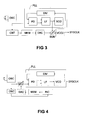
- the spread spectrum oscillator shown in FIG. 3 contains an oscillator OSC, a PLL PLL, a counter CNT, a memory device formed, for example, by a ROM MEM, a D / A converter DAC, a summation element SUM, and a second voltage controlled oscillator VCO2.
- the oscillator OSC and the PLL PLL are the oscillator OSC and the PLL of the clock signal generating device shown in FIG. 1. For more details on this reference is made to the explanations relating to FIG. 1.
- the counter CNT receives the input signal from the oscillator OSC output clock signal and gives the count to the MEM memory off.
- the memory MEM uses that from the counter CNT output count as address, and returns the under data stored in this address to the D / A converter DAC out.
- the D / A converter subjects the data supplied to it a D / A conversion and gives the result of this D / A conversion to the summation element SUM.
- the summation element SUM is in addition, the output signal of the loop filter LF PLL fed.
- the summation element sums the supplied ones Signals and gives the resulting signal as Control signal to the second voltage controlled oscillator VCO2 off.
- the clock signal is that of the second voltage-controlled oscillator VCO2 output clock signal.
- This second voltage controlled VCO2 oscillator has the same fundamental frequency as the voltage controlled oscillator VCO of the PLL, and will like this also using the output signal of the loop filter LF controlled.
- the second voltage controlled oscillator VCO2 control voltage also depends on it also from one through the counter CNT, the storage device MEM, and the D / A converter DAC formed offset; that controls the second voltage controlled oscillator VCO2 Control voltage is the output signal of the summation element SUM.
- the summation of the said offset to the output signal of the Loop Filter LF means that the second voltage controlled oscillator VCO2 output clock signal compared to that output by the voltage controlled oscillator VCO Clock signal is deliberately out of tune.
- the offset is the output of a frequency-modulated Signals from the second voltage controlled Oscillator VCO2 causes, whereby both the Modulation frequency and the modulation stroke specified become.
- the modulation frequency is determined by the counter CNT. As already mentioned above, the counter CNT was addressed, the memory MEM, in which in discrete Shape the modulation curve shape is saved.
- the modulation stroke can be selected both by the range of values in the memory MEM as well as by the signal swing of the Digital-to-analog converter DAC can be determined. realistic Values are between 0.1% and 1% of the system cycle.
- the spread spectrum oscillator described has the disadvantage on that its implementation is relatively complex, and that for practical implementation in an integrated circuit relatively much space is required, so that a integrated such spread spectrum oscillator Circuit becomes big and expensive.
- the present invention is therefore based on the object a simple and smaller realizable spread spectrum oscillator to accomplish.
- the clock signal generating device draws is characterized in that between the oscillator and the PLL a phase shift device is provided which the edges of the signal output by the oscillator in time can shift variable scope, and that from it resulting signal of the PLL as an input signal.
- the claimed clock signal generating device does not contains second voltage controlled oscillator, but "only" a phase shift device with controllable Phase shift, it is easier and less realizable than conventional spread spectrum oscillators.
- the clock signal generating device described below is part of a program-controlled with the exception of the oscillator Unit such as a microprocessor a microcontroller or a signal processor. It is already pointed out at this point that the described clock signal generating device also part of any other building block, and also a own module can be without further components.
- the Clock signal generating device can also be used as a discrete circuit be constructed.
- the clock signal generating device can both this containing programmable unit as well as others Supply system components with the clock signal generated by them; the program-controlled unit preferably contains an output terminal through which that from the clock signal generating means generated clock signal from the program-controlled Unit can be spent.
- the clock signal generating device presented here is a Spread spectrum oscillator with a simplified structure.
- the basic structure is shown in Figure 4.
- the clock signal generating device shown in FIG. 4 contains an oscillator OSC, a PLL PLL, one in the considered Example using a voltage-controlled delay element VCD formed phase shift device with controllable phase shift, a second frequency divider DIV2, an incrementer INC, one preferably through a non-volatile memory such as a ROM formed memory MEM, and a D / A converter DAC.
- the oscillator OSC and the PLL PLL are the oscillator OSC and the PLL of the clock signal generating device shown in FIG. 1 or components corresponding to them. In terms of Further details on this are provided on the Figure 1 referenced explanations.
- the voltage controlled delay element VCD is between the oscillator OSC and the PLL. That is, from Oscillator OSC generated clock signal is different from that in 1 and 3 clock signal generating devices shown the PLL not directly, but via the voltage-controlled Delay element VCD supplied.
- the voltage controlled Delay element VCD is caused by the output signal of the D / A converter DAC controlled.
- the one output by the DAC converter Signal is the result of D / A conversion from memory MEM output data.
- the memory MEM is determined by the output signal of the incrementer acting as an address generation device INC addressed.
- the incrementer INC is through the output signal of the second frequency divider DIV2 is driven.
- the second frequency divider DIV2 receives as an input signal the clock signal output by the oscillator OSC and generates from it a clock signal whose frequency is around a certain one Factor is less than the frequency of the output signal of the oscillator OSC.
- the control signals are stored in memory MEM in digital form, using which the voltage controlled Delay element VCD must be controlled in order for this supplied signal, more precisely its edges as desired to delay.
- the second frequency divider DIV2 and Incrementing device INC ensures that the Memory MEM outputs the control signal at the desired time, using the voltage controlled delay element VCD must be controlled so that it is the respective performs the desired delay.
- the voltage-controlled delay element VCD is controlled so that the output from it, fed to the PLL Signal which causes the PLL to a clock signal with varying Generate frequency. This happens because the voltage controlled delay element VCD the rising and falling edges of the clock signal output by the oscillator OSC so delayed that the PLL is supplied with a clock signal whose frequency appears to vary. The frequency of the output by the voltage-controlled delay element VCD However, the clock signal does not actually change; the PLL is cleverly shifted by a phase shift in its clock signal supplied by the voltage-controlled delay element just faked a frequency variation.
- the PLL a clock signal with varying frequency to feed the PLL to output a clock signal with varying Frequency to cause, because the readjustment of the Frequency of the clock signal output by the PLL SYSCLK takes place yes not dependent on the frequency difference, but depending on the phase difference of the phase comparator PD supplied signals.
- the voltage-controlled Delay element VCD every edge of the output from the oscillator OSC Clock signal for a certain time more or less delayed than the previous edge. It must be noted be that a clock edge of the output from the oscillator Clock signal must not be delayed to the extent that it is from the clock edge of the output signal fed back to the phase detector PD of the voltage-controlled oscillator VCO overhauled becomes.
- the maximum allowable time difference is between an edge of the output from the oscillator Clock signal and that of the voltage-controlled oscillator VCO output signal equals approximately one clock period. Becomes only one clock edge from the voltage-controlled delay element VCD (rising or falling) delayed, the permissible time difference over half a cycle period.
- the voltage-controlled delay element VCD can also a clock signal is generated for a certain (short) time, whose frequency actually (not only apparently) around constant is a certain amount greater or less than the frequency of the oscillator signal supplied to it.
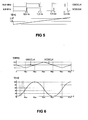
- FIG. 5 shows an example of how the flanks of an oscillator signal with a frequency of 10 MHz to delay the voltage-controlled delay element VCD are making this a signal with a constant frequency outputs from 9.9 MHz.
- the oscillator signal is OSCCLK shown. Below that is the voltage controlled delay element VCD output clock signal VCDCLK shown, and at the very bottom is the course of the delay V, with which the voltage controlled delay element VCD the edges occurring in the oscillator signal each has delayed.
- the first is increasing Edge of the oscillator signal is delayed by 0.5 ns, which points to it following falling edge by 0.5 ns more, i.e. delayed by 1.0 ns, the subsequent rising edge again by 0.5 ns more, i.e. delayed by 1.5 ns, the following falling Flank again by 0.5 ns more, i.e. delayed by 2.0 ns, etc.
- each clock period is 1 ns shorter than that previous clock period. Because the period of a signal with a frequency of 10 MHz is 100 ns, meet 100 clock periods the clock edges of the oscillator signal and that generated by the voltage-controlled delay element VCD Clock signal to each other. The phase relationship is then correct no more and the voltage controlled delay element VCD provides incorrect information at the exit.
- FIG. 6 An example of this is illustrated in FIG. 6.
- the example shown in FIG. 6 illustrates one triangular frequency modulation of the oscillator signal OSCCLK, the frequency of which may again be 10 MHz.
- the modulation swing is 100 kHz, which means the frequency of the voltage controlled delay element VCD generated clock signal between 9.9 MHz and VCDCLK 10.1 MHz oscillates.
- the modulation frequency was chosen to be 25 kHz, which corresponds to a period of 40 ⁇ s. Consequently must be the frequency of the voltage-controlled delay element VCD generated clock signal within 10 ⁇ s of 10.0 MHz drop to 9.9 MHz, then within 20 ⁇ s again increase from 9.9 MHz to 10.1 MHz, then in a further 20 ⁇ s drop again from 10.1 MHz to 9.9 MHz, and so on.
- the temporal course of the frequency of this clock signal is in the upper Diagram of Figure 6 illustrates.
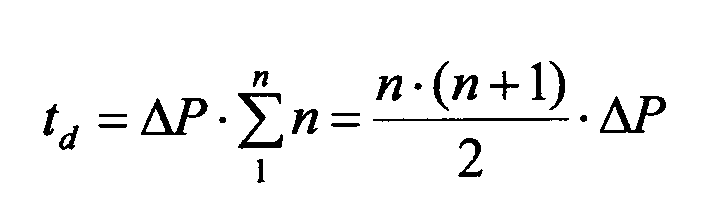
- ⁇ P 1 f osc - 1 f osc - f stroke
- the per cycle period (100th ns) the delay to be added gradually decreases again, so that the resulting frequency increases. Due to the Symmetry of the modulation curve must be the delay per clock period reduced by 10 ps plus the previous reduction that is successively around 10 ps, 20 ps, 30 ps and so further.
- the additional delay to be set absolutely in the VCD thereby increases by 10 ps, 30 ps, 60 ps, 100 ps and so further per clock period (100 ns). Even so, the overall delay the VCD is still larger, but from the clock period at clock period by a decreasing amount. After a further 10 ⁇ s, the value for the one to be added thus becomes Delay reached. Then the delay real diminished again.
- the changes and absolute values of the delay times to be set per clock period in the voltage-controlled delay element VCD are listed in the following table.
- the table covers a complete period of the modulation signal which, with a duration of 40 ⁇ s, comprises exactly 400 clock periods of the oscillator signal.
- the maximum value to be set for the delay time is 101 ns. It should be noted that this calculation was made for a control, but not for a regulation in the sense of a PLL.
- the feedback within the PLL is aimed at compensating for the edge delay, which ultimately leads to a reduction in the delay time actually to be set in the VCD. This effect was confirmed by analog simulations of the complete circuit. time [Microseconds] Oscillator signal period no.
- phase shift device not necessarily by a delay element, and certainly not by a voltage controlled delay element are formed got to. But it is important that it is a phase shift device deals with controllable phase shift.
- the clock signal generating device described can be regardless of the details of practical implementation easier and smaller than conventional ones
- Clock signal generating devices is the case that as Spread spectrum oscillators can be used.
- a controllable phase shift device is significant easier and smaller to implement than an additional voltage-controlled one Oscillator.
Landscapes
- Engineering & Computer Science (AREA)
- Computer Networks & Wireless Communication (AREA)
- Signal Processing (AREA)
- Physics & Mathematics (AREA)
- Nonlinear Science (AREA)
- Stabilization Of Oscillater, Synchronisation, Frequency Synthesizers (AREA)
Abstract
Description
- ganz oben für ein Taktsignal mit einer konstanten Frequenz f1,
- darunter für ein Taktsignal mit einer konstanten Frequenz f2,
- darunter für ein Taktsignal mit einer konstanten Frequenz f3,
- darunter für ein Taktsignal mit einer konstanten Frequenz f4, und
- ganz unten für ein Taktsignal mit zwischen f1 und f4 variierender Frequenz.
- Figur 1
- eine herkömmliche Taktsignalerzeugungseinrichtung zur Erzeugung eines Taktsignals mit konstanter Frequenz,
- Figur 2
- den zeitlichen Verlauf und das Frequenzspektrum von verschiedenen Taktsignalen,
- Figur 3
- eine herkömmliche Taktsignalerzeugungseinrichtung zur Erzeugung eines Taktsignals mit variierender Frequenz,
- Figur 4
- die im folgenden näher beschriebene Taktsignalerzeugungseinrichtung,
- Figur 5
- eine Darstellung zur Veranschaulichung der Phasenverschiebung, die eine Phasenverschiebungseinrichtung der Taktsignalerzeugungseinrichtung gemäß Figur 4 durchführen muß, um ein Taktsignal mit einer gegenüber dem ihr zugeführten Taktsignal konstant reduzierten Frequenz zu erzeugen, und
- Figur 6
- eine Darstellung zur Veranschaulichung der Phasenverschiebung, die die Phasenverschiebungseinrichtung durchführen muß, damit die Taktsignalerzeugungseinrichtung ein Taktsignal mit variierender Frequenz erzeugt.
ΔP = 10 ps; td = 50,5 ns.
| Zeit [µs] | Oszillatorsignal-Periode Nr. | td Änderung [ps] | td absolut [ps] | resultierende Frequenz [MHz] |
| 0 | 0 | 0 | 0 | 10,000 |
| 0,1 | 1 | 10 | 10 | 9,999 |
| 0,2 | 2 | 20 | 30 | 9,998 |
| 0,3 | 3 | 30 | 60 | 9,997 |
| ... | ||||
| 9,8 | 98 | 980 | 48530 | 9,902 |
| 9,9 | 99 | 990 | 49510 | 9,901 |
| 10,0 | 100 | 1000 | 50500 | 9,900 |
| 10,1 | 101 | 990 | 51490 | 9,901 |
| 10,2 | 102 | 980 | 52470 | 9,902 |
| ... | ||||
| 19,8 | 198 | 20 | 100970 | 9,998 |
| 19,9 | 199 | 10 | 100990 | 9,999 |
| 20,0 | 200 | 0 | 101000 | 10,000 |
| 20,1 | 201 | -10 | 100990 | 10,001 |
| 20,2 | 202 | -20 | 100970 | 10,002 |
| ... | ||||
| 29,8 | 298 | -980 | 52470 | 10,098 |
| 29,9 | 299 | -990 | 51490 | 10,099 |
| 30,0 | 300 | -1000 | 50500 | 10,100 |
| 30,1 | 301 | -990 | 49510 | 10,099 |
| 30,2 | 302 | -980 | 48530 | 10,098 |
| ... | ||||
| 39,8 | 398 | -20 | 30 | 10,002 |
| 39,9 | 399 | -10 | 10 | 10,001 |
| 40,0 | 400 | 0 | 0 | 10,000 |
| 40,1 | 401 | 10 | 10 | 9,999 |
| 40,2 | 402 | 20 | 30 | 9,998 |
| ... |
- daß die Frequenz des Oszillatorsignals 10 MHz beträgt,
- daß eine dreieckförmige Modulation durchgeführt wird,
- daß der Modulationshub 100 kHz beträgt, und
- daß die Modulationsfrequenz 25 kHz beträgt.
- CNT
- Zähler
- DAC
- D/A-Wandler
- DIV
- Frequenzteiler
- DIV2
- zweiter Frequenzteiler
- INC
- Inkrementierungseinrichtung, Adreßgenerierungseinrichtung
- LF
- Loop Filter
- MEM
- Speicher
- OSC
- Oszillator
- OSCCLK
- Ausgangssignal von OSC
- PD
- Phasenvergleicher
- PLL
- PLL
- SUM
- Summationsglied
- V
- Verzögerung
- VCD
- spannungsgesteuertes Verzögerungsglied
- VCDCLK
- Ausgangssignal von VCD
- VCO
- spannungsgesteuerter Oszillator
- VCO2
- zweiter spannungsgesteuerter Oszillator
Claims (10)
- Taktsignalerzeugungseinrichtung mit einem Oszillator (OSC) und einer diesem nachgeschalteten PLL (PLL),
dadurch gekennzeichnet, daß zwischen dem Oszillator (OSC) und der PLL (PLL) eine Phasenverschiebungseinrichtung (VCD) vorgesehen ist, welche die Flanken des vom Oszillator (OSC) ausgegebenen Signals in zeitlich variierbarem Umfang verschieben kann, und das daraus resultierende Signal der PLL (PLL) als Eingangssignal zuführt. - Taktsignalerzeugungseinrichtung nach Anspruch 1,
dadurch gekennzeichnet, daß die Phasenverschiebungseinrichtung (VCD) durch ein Verzögerungsglied mit einstellbarer Verzögerung gebildet wird. - Taktsignalerzeugungseinrichtung nach Anspruch 1 oder 2,
dadurch gekennzeichnet, daß die Phasenverschiebungseinrichtung (VCD) durch ein spannungsgesteuertes Verzögerungsglied gebildet wird. - Taktsignalerzeugungseinrichtung nach einem der vorhergehenden Ansprüche,
dadurch gekennzeichnet, daß die Steuersignale, unter Verwendung welcher die Phasenverschiebungseinrichtung (VCD) angesteuert wird, in einer Speichereinrichtung (MEM) gespeichert sind. - Taktsignalerzeugungseinrichtung nach Anspruch 4,
dadurch gekennzeichnet, daß die Speichereinrichtung (MEM) durch eine nichtflüchtige Speichereinrichtung gebildet wird. - Taktsignalerzeugungseinrichtung nach Anspruch 4 oder 5,
dadurch gekennzeichnet, daß die Speichereinrichtung (MEM) durch eine Adreßgenerierungseinrichtung (INC) adressiert wird, welche die jeweils zu verwendende Adresse unter Berücksichtigung des Ausgangssignals eines die Frequenz des Ausgangssignals des Oszillators (OSC) teilenden Frequenzteilers (DIV2) generiert. - Taktsignalerzeugungseinrichtung nach Anspruch 6,
dadurch gekennzeichnet, daß das aus der Speichereinrichtung (MEM) ausgegebene Steuersignal der Phasenverschiebungseinrichtung (VCD) über einen D/A-Wandler zugeführt wird, welche den von der Speichereinrichtung (MEM) ausgegebenen Wert in ein analoges Steuersignal umwandelt. - Taktsignalerzeugungseinrichtung nach einem der vorhergehenden Ansprüche,
dadurch gekennzeichnet, daß die Phasenverschiebungseinrichtung (VCD) so angesteuert wird, daß die PLL (PLL) ein Taktsignal (SYSCLK) mit variierender Frequenz erzeugt. - Taktsignalerzeugungseinrichtung nach einem der vorhergehenden Ansprüche,
dadurch gekennzeichnet, daß die Phasenverschiebungseinrichtung (VCD) so angesteuert wird, daß die Taktsignalerzeugungseinrichtung als Spread Spectrum Oszillator verwendbar ist. - Taktsignalerzeugungseinrichtung nach einem der vorhergehenden Ansprüche,
dadurch gekennzeichnet, daß die Phasenverschiebungseinrichtung (VCD) so angesteuert wird, daß sie die Flanken des ihr vom Oszillator (OSC) zugeführten Taktsignals so verschiebt, daß das von der Phasenverschiebungseinrichtung (VCD) ausgegebene Taktsignal eine andere Frequenz aufweist als das vom Oszillator (OSC) ausgegebene Taktsignal.
Priority Applications (2)
| Application Number | Priority Date | Filing Date | Title |
|---|---|---|---|
| EP02002307.3A EP1333581B1 (de) | 2002-01-30 | 2002-01-30 | Taktsignalerzeugungseinrichtung |
| US10/356,922 US6798303B2 (en) | 2002-01-30 | 2003-01-30 | Clock signal generating device |
Applications Claiming Priority (1)
| Application Number | Priority Date | Filing Date | Title |
|---|---|---|---|
| EP02002307.3A EP1333581B1 (de) | 2002-01-30 | 2002-01-30 | Taktsignalerzeugungseinrichtung |
Publications (2)
| Publication Number | Publication Date |
|---|---|
| EP1333581A1 true EP1333581A1 (de) | 2003-08-06 |
| EP1333581B1 EP1333581B1 (de) | 2015-04-08 |
Family
ID=8185390
Family Applications (1)
| Application Number | Title | Priority Date | Filing Date |
|---|---|---|---|
| EP02002307.3A Expired - Lifetime EP1333581B1 (de) | 2002-01-30 | 2002-01-30 | Taktsignalerzeugungseinrichtung |
Country Status (2)
| Country | Link |
|---|---|
| US (1) | US6798303B2 (de) |
| EP (1) | EP1333581B1 (de) |
Families Citing this family (7)
| Publication number | Priority date | Publication date | Assignee | Title |
|---|---|---|---|---|
| US7561652B2 (en) * | 2003-04-22 | 2009-07-14 | Paul Kevin Hall | High frequency spread spectrum clock generation |
| US7741815B2 (en) * | 2005-11-07 | 2010-06-22 | General Electric Company | Lithium polymer battery powered intravenous fluid warmer |
| JP2007251925A (ja) * | 2006-02-20 | 2007-09-27 | Nec Saitama Ltd | クロック生成回路 |
| US7504897B2 (en) * | 2006-10-30 | 2009-03-17 | Agere Systems Inc. | Switched-current oscillator for clock-frequency spreading |
| RU2319300C1 (ru) * | 2006-11-21 | 2008-03-10 | Институт радиотехники и электроники Российской Академии Наук | Широкополосная система фазовой автоподстройки частоты для криогенного генератора |
| US8326593B1 (en) * | 2010-05-25 | 2012-12-04 | Cadence Design Systems, Inc. | Amplitude modulation-phase modulation decomposition method for phase noise simulation of oscillators with large time-constant |
| EP3477864B1 (de) * | 2017-10-31 | 2020-07-08 | Nxp B.V. | Vorrichtung mit einer phasenregelschleife |
Citations (3)
| Publication number | Priority date | Publication date | Assignee | Title |
|---|---|---|---|---|
| EP0319851A1 (de) * | 1987-12-08 | 1989-06-14 | TELEFUNKEN Sendertechnik GmbH | Digitale Phaseneinstellung für digital generierte Signale |
| JP2000101424A (ja) * | 1998-09-18 | 2000-04-07 | Sony Corp | クロック発生回路 |
| US6160456A (en) * | 1999-06-14 | 2000-12-12 | Realtek Semiconductor Corp. | Phase-locked loop having adjustable delay elements |
Family Cites Families (4)
| Publication number | Priority date | Publication date | Assignee | Title |
|---|---|---|---|---|
| US5488627A (en) | 1993-11-29 | 1996-01-30 | Lexmark International, Inc. | Spread spectrum clock generator and associated method |
| US5631920A (en) | 1993-11-29 | 1997-05-20 | Lexmark International, Inc. | Spread spectrum clock generator |
| US5491458A (en) * | 1994-11-08 | 1996-02-13 | Mccune, Jr.; Earl W. | Apparatus for spreading the spectrum of a signal and method therefor |
| US6167103A (en) | 1998-10-08 | 2000-12-26 | Lexmark International, Inc. | Variable spread spectrum clock |
-
2002
- 2002-01-30 EP EP02002307.3A patent/EP1333581B1/de not_active Expired - Lifetime
-
2003
- 2003-01-30 US US10/356,922 patent/US6798303B2/en not_active Expired - Lifetime
Patent Citations (3)
| Publication number | Priority date | Publication date | Assignee | Title |
|---|---|---|---|---|
| EP0319851A1 (de) * | 1987-12-08 | 1989-06-14 | TELEFUNKEN Sendertechnik GmbH | Digitale Phaseneinstellung für digital generierte Signale |
| JP2000101424A (ja) * | 1998-09-18 | 2000-04-07 | Sony Corp | クロック発生回路 |
| US6160456A (en) * | 1999-06-14 | 2000-12-12 | Realtek Semiconductor Corp. | Phase-locked loop having adjustable delay elements |
Non-Patent Citations (1)
| Title |
|---|
| PATENT ABSTRACTS OF JAPAN vol. 2000, no. 07 29 September 2000 (2000-09-29) * |
Also Published As
| Publication number | Publication date |
|---|---|
| EP1333581B1 (de) | 2015-04-08 |
| US6798303B2 (en) | 2004-09-28 |
| US20030141937A1 (en) | 2003-07-31 |
Similar Documents
| Publication | Publication Date | Title |
|---|---|---|
| EP0408983B1 (de) | Frequenzsynthesizer | |
| EP0715408B1 (de) | Taktgenerator zur Erzeugung eines störstrahlungsarmen Systemtaktes | |
| DE69700270T2 (de) | Frequenzvervielfacher, bei dem das Multiplikationsverhältnis in der ersten Stufe grösser ist als in den nachfolgenden Stufen | |
| DE69633651T2 (de) | Taktgenerator mit spektraler Dispersion | |
| DE60008203T2 (de) | Phasenregelschleife mit digital gesteuertem frequenzvervielfachendem Oszillator | |
| EP2421154B1 (de) | Schaltungsanordnung zur Erzeugung von eine breitbandige Frequenzrampe bildenden hochfrequenten Ausgangssignalen | |
| DE69031738T2 (de) | Spannungsgesteuerter Oszillator | |
| DE60219527T2 (de) | Takterzeugungsschaltung | |
| DE102006052873A1 (de) | Filter-Schaltungsanordnung | |
| DE202016105147U1 (de) | Spektrumsspreizungstaktgeber | |
| DE69321008T2 (de) | Frequenzsynthetisierer mit gebrochenem Teilverhältnis mit Digitalfehlerkorrektion | |
| DE1964912B2 (de) | Frequenz-Synthesizer | |
| DE1959162C3 (de) | Stufenweise nach einem Frequenzraster einstellbarer Frequenzgenerator | |
| EP0828360A1 (de) | Taktgenerator zur Erzeugung eines störstrahlarmen Systemtaktes | |
| EP2664068B1 (de) | Hochfrequenzgenerator mit geringem phasenrauschen | |
| EP1333581B1 (de) | Taktsignalerzeugungseinrichtung | |
| DE69824114T2 (de) | Phasenregelkreis und Verfahren zum Steuern des Phasenregelkreises | |
| DE69710165T2 (de) | Phasenregelschleife | |
| DE1766866B1 (de) | Frequenzsynthetisator unter verwendung von regelschleifen | |
| EP0166749B1 (de) | Phasenregelkreis | |
| DE102006050881B3 (de) | Phasen-/Frequenzvergleicher, Phasenregelkreis, Verfahren zur Phasen-/Frequenzdetektion und Verfahren zum Erzeugen eines Oszillatorsignals | |
| DE102007001148A1 (de) | Phasenregelschleife zum schnellen Einregeln und darauf bezogenes Verfahren | |
| WO2004068697A1 (de) | Vorrichtung und verfahren zur frequenzsynthese | |
| EP4187780A1 (de) | Frequenzgeneratoranordnung mir leistungsregelkeis | |
| DE102004059987B4 (de) | Spannungsgesteuerte Oszillatorschaltung mit analoger und digitaler Ansteuerung und phasenverriegelte Regelschleife mit einer solchen Oszillatorschaltung |
Legal Events
| Date | Code | Title | Description |
|---|---|---|---|
| PUAI | Public reference made under article 153(3) epc to a published international application that has entered the european phase |
Free format text: ORIGINAL CODE: 0009012 |
|
| AK | Designated contracting states |
Designated state(s): AT BE CH CY DE DK ES FI FR GB GR IE IT LI LU MC NL PT SE TR |
|
| AX | Request for extension of the european patent |
Extension state: AL LT LV MK RO SI |
|
| 17P | Request for examination filed |
Effective date: 20040205 |
|
| AKX | Designation fees paid |
Designated state(s): DE FR IT |
|
| RAP1 | Party data changed (applicant data changed or rights of an application transferred) |
Owner name: INFINEON TECHNOLOGIES AG |
|
| REG | Reference to a national code |
Ref country code: DE Ref legal event code: R079 Ref document number: 50216034 Country of ref document: DE Free format text: PREVIOUS MAIN CLASS: H03L0007081000 Ipc: H03K0005159000 |
|
| RIC1 | Information provided on ipc code assigned before grant |
Ipc: H04B 15/04 20060101ALI20140904BHEP Ipc: H03L 7/081 20060101ALI20140904BHEP Ipc: H03K 5/159 20060101AFI20140904BHEP Ipc: H03K 7/06 20060101ALI20140904BHEP |
|
| GRAP | Despatch of communication of intention to grant a patent |
Free format text: ORIGINAL CODE: EPIDOSNIGR1 |
|
| INTG | Intention to grant announced |
Effective date: 20141021 |
|
| GRAS | Grant fee paid |
Free format text: ORIGINAL CODE: EPIDOSNIGR3 |
|
| GRAA | (expected) grant |
Free format text: ORIGINAL CODE: 0009210 |
|
| AK | Designated contracting states |
Kind code of ref document: B1 Designated state(s): DE FR IT |
|
| REG | Reference to a national code |
Ref country code: DE Ref legal event code: R096 Ref document number: 50216034 Country of ref document: DE Effective date: 20150513 |
|
| REG | Reference to a national code |
Ref country code: DE Ref legal event code: R097 Ref document number: 50216034 Country of ref document: DE |
|
| PLBE | No opposition filed within time limit |
Free format text: ORIGINAL CODE: 0009261 |
|
| STAA | Information on the status of an ep patent application or granted ep patent |
Free format text: STATUS: NO OPPOSITION FILED WITHIN TIME LIMIT |
|
| 26N | No opposition filed |
Effective date: 20160111 |
|
| PG25 | Lapsed in a contracting state [announced via postgrant information from national office to epo] |
Ref country code: IT Free format text: LAPSE BECAUSE OF FAILURE TO SUBMIT A TRANSLATION OF THE DESCRIPTION OR TO PAY THE FEE WITHIN THE PRESCRIBED TIME-LIMIT Effective date: 20150408 |
|
| REG | Reference to a national code |
Ref country code: FR Ref legal event code: ST Effective date: 20160930 |
|
| PG25 | Lapsed in a contracting state [announced via postgrant information from national office to epo] |
Ref country code: FR Free format text: LAPSE BECAUSE OF NON-PAYMENT OF DUE FEES Effective date: 20160201 |
|
| PGFP | Annual fee paid to national office [announced via postgrant information from national office to epo] |
Ref country code: DE Payment date: 20190321 Year of fee payment: 18 |
|
| REG | Reference to a national code |
Ref country code: DE Ref legal event code: R119 Ref document number: 50216034 Country of ref document: DE |
|
| PG25 | Lapsed in a contracting state [announced via postgrant information from national office to epo] |
Ref country code: DE Free format text: LAPSE BECAUSE OF NON-PAYMENT OF DUE FEES Effective date: 20200801 |