EP1331660A2 - Polycrystalline silicon thin film for a thin film transistor and display device using the same - Google Patents
Polycrystalline silicon thin film for a thin film transistor and display device using the same Download PDFInfo
- Publication number
- EP1331660A2 EP1331660A2 EP02090404A EP02090404A EP1331660A2 EP 1331660 A2 EP1331660 A2 EP 1331660A2 EP 02090404 A EP02090404 A EP 02090404A EP 02090404 A EP02090404 A EP 02090404A EP 1331660 A2 EP1331660 A2 EP 1331660A2
- Authority
- EP
- European Patent Office
- Prior art keywords
- tft
- thin film
- polycrystalline silicon
- silicon thin
- crystal grain
- Prior art date
- Legal status (The legal status is an assumption and is not a legal conclusion. Google has not performed a legal analysis and makes no representation as to the accuracy of the status listed.)
- Withdrawn
Links
Images


Classifications
-
- H—ELECTRICITY
- H10—SEMICONDUCTOR DEVICES; ELECTRIC SOLID-STATE DEVICES NOT OTHERWISE PROVIDED FOR
- H10D—INORGANIC ELECTRIC SEMICONDUCTOR DEVICES
- H10D30/00—Field-effect transistors [FET]
- H10D30/60—Insulated-gate field-effect transistors [IGFET]
- H10D30/67—Thin-film transistors [TFT]
-
- H—ELECTRICITY
- H10—SEMICONDUCTOR DEVICES; ELECTRIC SOLID-STATE DEVICES NOT OTHERWISE PROVIDED FOR
- H10D—INORGANIC ELECTRIC SEMICONDUCTOR DEVICES
- H10D86/00—Integrated devices formed in or on insulating or conducting substrates, e.g. formed in silicon-on-insulator [SOI] substrates or on stainless steel or glass substrates
- H10D86/01—Manufacture or treatment
- H10D86/021—Manufacture or treatment of multiple TFTs
- H10D86/0221—Manufacture or treatment of multiple TFTs comprising manufacture, treatment or patterning of TFT semiconductor bodies
- H10D86/0223—Manufacture or treatment of multiple TFTs comprising manufacture, treatment or patterning of TFT semiconductor bodies comprising crystallisation of amorphous, microcrystalline or polycrystalline semiconductor materials
- H10D86/0229—Manufacture or treatment of multiple TFTs comprising manufacture, treatment or patterning of TFT semiconductor bodies comprising crystallisation of amorphous, microcrystalline or polycrystalline semiconductor materials characterised by control of the annealing or irradiation parameters
-
- H—ELECTRICITY
- H10—SEMICONDUCTOR DEVICES; ELECTRIC SOLID-STATE DEVICES NOT OTHERWISE PROVIDED FOR
- H10D—INORGANIC ELECTRIC SEMICONDUCTOR DEVICES
- H10D30/00—Field-effect transistors [FET]
- H10D30/01—Manufacture or treatment
- H10D30/021—Manufacture or treatment of FETs having insulated gates [IGFET]
- H10D30/031—Manufacture or treatment of FETs having insulated gates [IGFET] of thin-film transistors [TFT]
- H10D30/0312—Manufacture or treatment of FETs having insulated gates [IGFET] of thin-film transistors [TFT] characterised by the gate electrodes
-
- H—ELECTRICITY
- H10—SEMICONDUCTOR DEVICES; ELECTRIC SOLID-STATE DEVICES NOT OTHERWISE PROVIDED FOR
- H10D—INORGANIC ELECTRIC SEMICONDUCTOR DEVICES
- H10D30/00—Field-effect transistors [FET]
- H10D30/01—Manufacture or treatment
- H10D30/021—Manufacture or treatment of FETs having insulated gates [IGFET]
- H10D30/031—Manufacture or treatment of FETs having insulated gates [IGFET] of thin-film transistors [TFT]
- H10D30/0321—Manufacture or treatment of FETs having insulated gates [IGFET] of thin-film transistors [TFT] comprising silicon, e.g. amorphous silicon or polysilicon
-
- H—ELECTRICITY
- H10—SEMICONDUCTOR DEVICES; ELECTRIC SOLID-STATE DEVICES NOT OTHERWISE PROVIDED FOR
- H10D—INORGANIC ELECTRIC SEMICONDUCTOR DEVICES
- H10D30/00—Field-effect transistors [FET]
- H10D30/60—Insulated-gate field-effect transistors [IGFET]
- H10D30/67—Thin-film transistors [TFT]
- H10D30/6729—Thin-film transistors [TFT] characterised by the electrodes
- H10D30/673—Thin-film transistors [TFT] characterised by the electrodes characterised by the shapes, relative sizes or dispositions of the gate electrodes
- H10D30/6733—Multi-gate TFTs
-
- H—ELECTRICITY
- H10—SEMICONDUCTOR DEVICES; ELECTRIC SOLID-STATE DEVICES NOT OTHERWISE PROVIDED FOR
- H10D—INORGANIC ELECTRIC SEMICONDUCTOR DEVICES
- H10D30/00—Field-effect transistors [FET]
- H10D30/60—Insulated-gate field-effect transistors [IGFET]
- H10D30/67—Thin-film transistors [TFT]
- H10D30/674—Thin-film transistors [TFT] characterised by the active materials
- H10D30/6741—Group IV materials, e.g. germanium or silicon carbide
- H10D30/6743—Silicon
- H10D30/6745—Polycrystalline or microcrystalline silicon
-
- H—ELECTRICITY
- H10—SEMICONDUCTOR DEVICES; ELECTRIC SOLID-STATE DEVICES NOT OTHERWISE PROVIDED FOR
- H10D—INORGANIC ELECTRIC SEMICONDUCTOR DEVICES
- H10D30/00—Field-effect transistors [FET]
- H10D30/60—Insulated-gate field-effect transistors [IGFET]
- H10D30/67—Thin-film transistors [TFT]
- H10D30/6757—Thin-film transistors [TFT] characterised by the structure of the channel, e.g. transverse or longitudinal shape or doping profile
-
- H—ELECTRICITY
- H10—SEMICONDUCTOR DEVICES; ELECTRIC SOLID-STATE DEVICES NOT OTHERWISE PROVIDED FOR
- H10D—INORGANIC ELECTRIC SEMICONDUCTOR DEVICES
- H10D62/00—Semiconductor bodies, or regions thereof, of devices having potential barriers
- H10D62/40—Crystalline structures
-
- H—ELECTRICITY
- H10—SEMICONDUCTOR DEVICES; ELECTRIC SOLID-STATE DEVICES NOT OTHERWISE PROVIDED FOR
- H10D—INORGANIC ELECTRIC SEMICONDUCTOR DEVICES
- H10D86/00—Integrated devices formed in or on insulating or conducting substrates, e.g. formed in silicon-on-insulator [SOI] substrates or on stainless steel or glass substrates
- H10D86/01—Manufacture or treatment
- H10D86/021—Manufacture or treatment of multiple TFTs
- H10D86/0251—Manufacture or treatment of multiple TFTs characterised by increasing the uniformity of device parameters
-
- H—ELECTRICITY
- H10—SEMICONDUCTOR DEVICES; ELECTRIC SOLID-STATE DEVICES NOT OTHERWISE PROVIDED FOR
- H10P—GENERIC PROCESSES OR APPARATUS FOR THE MANUFACTURE OR TREATMENT OF DEVICES COVERED BY CLASS H10
- H10P14/00—Formation of materials, e.g. in the shape of layers or pillars
- H10P14/20—Formation of materials, e.g. in the shape of layers or pillars of semiconductor materials
- H10P14/34—Deposited materials, e.g. layers
- H10P14/3402—Deposited materials, e.g. layers characterised by the chemical composition
- H10P14/3404—Deposited materials, e.g. layers characterised by the chemical composition being Group IVA materials
- H10P14/3411—Silicon, silicon germanium or germanium
-
- H—ELECTRICITY
- H10—SEMICONDUCTOR DEVICES; ELECTRIC SOLID-STATE DEVICES NOT OTHERWISE PROVIDED FOR
- H10P—GENERIC PROCESSES OR APPARATUS FOR THE MANUFACTURE OR TREATMENT OF DEVICES COVERED BY CLASS H10
- H10P14/00—Formation of materials, e.g. in the shape of layers or pillars
- H10P14/20—Formation of materials, e.g. in the shape of layers or pillars of semiconductor materials
- H10P14/34—Deposited materials, e.g. layers
- H10P14/3451—Structure
- H10P14/3452—Microstructure
- H10P14/3456—Polycrystalline
-
- H—ELECTRICITY
- H10—SEMICONDUCTOR DEVICES; ELECTRIC SOLID-STATE DEVICES NOT OTHERWISE PROVIDED FOR
- H10P—GENERIC PROCESSES OR APPARATUS FOR THE MANUFACTURE OR TREATMENT OF DEVICES COVERED BY CLASS H10
- H10P14/00—Formation of materials, e.g. in the shape of layers or pillars
- H10P14/20—Formation of materials, e.g. in the shape of layers or pillars of semiconductor materials
- H10P14/38—Formation of materials, e.g. in the shape of layers or pillars of semiconductor materials characterised by treatments done after the formation of the materials
- H10P14/3802—Crystallisation or recrystallisation of non-monocrystalline semiconductor materials, e.g. regrowth
- H10P14/3808—Crystallisation or recrystallisation of non-monocrystalline semiconductor materials, e.g. regrowth using laser beams
- H10P14/3816—Pulsed laser beam
Definitions
- the present invention relates to a polycrystalline silicon thin film for a thin film transistor and a display device using the same, and more particularly, to a polycrystalline silicon thin film for a thin film transistor with silicon grains in a crystal growing direction of which is constant and regularized, and a device using the thin film transistor fabricated using the polycrystalline silicon thin film.
- Bonding defects such as atom dangling bonds existing on the crystal grain boundaries of polycrystalline silicon included in an active channel region, are known to provide traps for electric charge carriers when fabricating a thin film transistor (TFT) substrate using polycrystalline silicon.
- TFT threshold voltage
- subthreshold slope charge carrier mobility
- leakage current leakage current and device stability
- uniformity in characteristics between TFTs is fatally influenced by the crystal grain boundaries, as the crystal grains are getting bigger and more regularized in order to improve TFT characteristics.
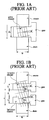
- TFT characteristics might be superior when fabricating a TFT using a dual or multiple active channel having the same active channel length, since the number of crystal grain boundaries fatally influencing movement of the electric charge carrier are reduced as compared to when fabricating a TFT comprising a single active channel.
- the number of the fatal crystal grain boundaries included in the active channel region is 3, and the total length of the channel is 2L.
- the number of the fatal crystal grain boundaries included in each of the channel regions might be 2 or 1 for a TFT comprising multiple channels (FIG. 1 B). Therefore, TFT characteristics will be improved as a whole when the fatal crystal grain boundaries acting as a barrier for movement of the electric charge carriers are decreased.
- the number of the fatal crystal grain boundaries included in each of the active channels can be varied depending on positions of the channel, but uniformity of the TFT may be deteriorated accordingly.
- one fatal crystal grain boundary is included in the first active channel while two fatal crystal grain boundaries are included in the second active channel.
- the SLS method of fabricating a TFT by forming single crystalline silicon has problems in that TFTs should be accurately aligned in an active channel region at positions where a plurality of TFTs on a substrate are technically difficult to fabricate, and a longer time is required in forming single crystalline silicon having a dimension corresponding to at least the active channel region, compared to when fabricating a TFT substrate using polycrystalline silicon.
- a SLS method of fabricating a TFT using polycrystalline silicon is known to be superior to the SLS method of fabricating a TFT by forming single crystalline silicon. This is a reason that when the TFT is fabricated by the SLS using single crystalline silicon, it takes more time to fabricate the TFT than the SLS method of fabricating the TFT using polycrystalline silicon. Accordingly, in the aspect of commercial production, a throughput of the SLS method using single crystalline is decreased.
- a TFT using single crystalline silicon can be required in fabricating an active matrix display, such as characteristics requiring a completely built-in driver circuit as well as a circuit requiring a TFT of high characteristics, such as a digital to analog converter (DAC) circuit.
- DAC digital to analog converter
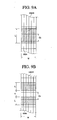
- the barrier effect of the crystal grain boundaries for electric carriers is minimized, as illustrated in FIG. 4A, when a direction of the active channel in fabricating a TFT for liquid crystal display (LCD) devices comprising a driver and pixel array by forming large silicon grains using SLS crystallization technology, is parallel to a direction of crystal grains grown by the SLS crystallization method. Therefore, TFT characteristics which are second to characteristics of single crystalline silicon can be obtained although these characteristics are greatly deteriorated, as illustrated in FIG. 4B, since many crystal grain boundaries acting as traps for electric charge carriers exist where a direction of the active channel is perpendicular to a growing direction of the crystal grains.
- a TFT inside the driver circuit usually has an angle of 90° when actually fabricating an active matrix display, wherein uniformity of the device can be improved by slantingly fabricating the active matrix display in such a way that a direction of the active channel region is inclined at a growing angle of the crystal grains by an angle of 30° to 60° to improve uniformity between TFTs while not greatly deteriorating characteristics of each TFT, as illustrated in FIG. 4C.
- Gs is a size of crystal grains of the polycrystalline silicon thin film
- m is an integer of 1 or more
- ⁇ is an inclined angle where fatal crystal grain boundaries, that is, "primary" crystal grain boundaries are inclined in a direction perpendicular to an active channel direction
- L represents a length of active channels for each TFT comprising dual or multiple channels.
- the foregoing and other objects of the present invention may also be achieved by providing a display device fabricated using the polycrystalline silicon thin film for the TFTs.
- a crystal grain boundary is formed between neighboring crystal grains due to a limited size of the crystal grains.
- crystal grains of polycrystalline silicon directly and indirectly exert important influence on TFT characteristics when fabricating a TFT for an active matrix display, they are enlarged and regularized to improve the TFT characteristics.
- a crystal grain boundary exerting a fatal influence on TFT characteristics when the crystal grain boundary exists in an active channel region particularly, a "primary" crystal grain boundary in which an inclined angle of the crystal grain boundary in a direction perpendicular to an active channel direction is -45 ° ⁇ ⁇ ⁇ 45°, as illustrated in FIG. 1A and FIG. 1B, contains inevitable defects due to the limit of processing accuracy during formation of a polycrystalline silicon thin film.
- the number of the "primary" crystal grain boundaries included in a TFT active channel region fabricated on a substrate or display may be variable depending on the size and direction of the crystal grains, and also depending on the dimension of the active channels, as illustrated in FIG. 4A to FIG. 4C.
- a size of the crystal grains that can be grown during formation of polycrystalline silicon is not only limited depending on thin film characteristics or thin film thickness according to formation methods of amorphous silicon, such as plasma enhanced chemical vapor deposition (PECVD), low pressure chemical vapor deposition (LPCVD) and sputtering, but is also directly influenced by the crystallization technology of phase-transforming the amorphous silicon into crystalline silicon.
- PECVD plasma enhanced chemical vapor deposition
- LPCVD low pressure chemical vapor deposition
- sputtering but is also directly influenced by the crystallization technology of phase-transforming the amorphous silicon into crystalline silicon.
- a maximum size of crystal grains that can be grown is determined by energy density, pulse duration, substrate conductivity and substrate temperature during silicon crystallization using laser energy (e.g. excimer laser annealing).
- laser energy e.g. excimer laser annealing
- an active channel dimension of a TFT used in an active matrix display is frequently larger than the size of the crystal grains. Accordingly, a fatal crystal grain boundary exerting an influence on TFT characteristics often exists in the active channel region, and TFT characteristics using polycrystalline silicon can be greatly deteriorated compared to TFT characteristics using single crystalline silicon, as illustrated in FIG. 5A.
- TFT characteristics can be improved, as illustrated in FIG. 5B, since the number of fatal crystal grain boundaries included in each of the channels is decreased by fabricating a TFT using dual gates or multiple gates to form dual or multiple channels having a length of 2L.
- the present invention provides that the number of fatal crystal grain boundaries included in neighboring active channels can be equalized so that the same characteristics can be obtained, as illustrated in FIG. 5C, when a distance between the dual gates or multiple gates is a multiple integer of a specific distance "S,” or more preferably, when the distance between the dual gates or multiple gates is the same as the distance "S.”
- a size of crystal grains means a specific distance between crystal grain boundaries, and is defined as a distance of the crystal grain boundaries within an ordinary error range.
- a crystal grain boundary forming an angle ⁇ of -45 ° ⁇ 45 ° with NN' can have fatal influence on movement of electric charge carriers, and the crystal grain boundary is defined as a "primary" crystal grain boundary, as illustrated in FIG 6A and FIG. 6B.
- a distance perpendicular to the "primary" crystal grain boundary for an active channel region having a length L and a width W that is, a maximum distance in the active channel region D, can be represented as follows by a simple trigonometrical function, as illustrated in FIG. 7.
- D L cos ⁇ + W sin ⁇ since tan ⁇ x cos ⁇ is sin ⁇ . That is, D can be represented by functions of a length L and a width W of the active channel region, and an inclined angle ⁇ of the "primary" crystal grain boundary for the normal line NN'.
- the distance S always should be S>0 so that the distance S is defined as dual gates or multiple gates having a physical distance, and therefore, the value of m for synchronization can be determined.
- ⁇ 0 °
- TFT characteristics are more preferable where an inclined angle of the crystal grain boundaries is -5° ⁇ ⁇ ⁇ 5°.
- TFT characteristics can become superior since the number of crystal grain boundaries exerting fatal influence on movement of electric charge carriers is reduced when fabricating a TFT using dual or multiple active channels having an equal active channel length, compared to when a TFT comprising a single active channel is fabricated using polycrystalline silicon crystal grains having a size which is constant in the total region or partial region on a TFT substrate or an active matrix display, and a growing direction which is constant and regularized in an active channel direction. Furthermore, uniformity of a TFT can be improved by synchronizing the number of fatal crystal grain boundaries included in each channel region of dual or multiple active channels when designing a TFT using a numerical formula defined in the present invention.
Landscapes
- Thin Film Transistor (AREA)
- Liquid Crystal (AREA)
- Recrystallisation Techniques (AREA)
- Devices For Indicating Variable Information By Combining Individual Elements (AREA)
Abstract
Description
In the case of = 0 °
Therefore, in the case that = 0 °, it can be understood that S = mGs - L.


Claims (14)
- A polycrystalline silicon thin film for a TFT having a distance "S" between active channels of the TFT comprising:where Gs is a size of crystal grains of the polycrystalline silicon thin film, m is an integer of 1 or more, is an inclined angle where fatal crystal grain boundaries are inclined in a direction perpendicular to an active channel direction, and L represents a length of active channels for each TFT comprising dual or multiple channels.dual or multiple channels having a relation according to the expression:
- The polycrystalline silicon thin film for the TFT of claim 1, wherein the distance between the dual or multiple channels is a multiple integer of "S" when is 0°.
- The polycrystalline silicon thin film for the TFT of claim 2, wherein the distance between the dual or multiple channels is the same as "S" when is 0 °.
- The polycrystalline silicon thin film for the TFT of claim 1, wherein the polycrystalline silicon film is formed on a total area of a substrate of a display device or a partial area of the substrate of the display device.
- The polycrystalline silicon thin film for the TFT of claim 1, wherein the size of the crystal grains is 0.2m or more.

- The polycrystalline silicon thin film for the TFT of claim 1, wherein two or more crystal grains are arranged on a substrate of the TFT.
- The polycrystalline silicon thin film for the TFT of claim 1, wherein the inclined angle of the fatal crystal grain boundaries is -45 ° ≤ ≤ 45°.
- The polycrystalline silicon thin film for the TFT of claim 7, wherein the inclined angle of the fatal crystal grain boundaries is -5 °≤ ≤ 5°.
- The polycrystalline silicon thin film for the TFT of claim 1, wherein the length of the active channels is a multiple integer of the size of the crystal grains.
- The polycrystalline silicon thin film for the TFT of claim 1, wherein the number of the crystal grains inside the display is two or more.
- The polycrystalline silicon thin film for the TFT of claim 1, wherein the crystal grains are grown in a contant direction.
- The polycrystalline silicon thin film for the TFT of claim 1, wherein the crystalline silicon film is formed by crystallizing amorphous silicon grown using a method selected from plasma enhanced chemical vapor deposition (PECVD), low pressure chemical vapor deposition (LPCVD) and sputtering in excimer laser annealing.
- A display device having a TFT which is fabricated using the polycrystalline thin film of claim 1.
- The device of claim 13, wherein the display device is a liquid crystal display or an organic electroluminescent device.
Applications Claiming Priority (2)
| Application Number | Priority Date | Filing Date | Title |
|---|---|---|---|
| KR2002003073 | 2002-01-18 | ||
| KR10-2002-0003073A KR100462862B1 (en) | 2002-01-18 | 2002-01-18 | Polysilicon thin layer for thin film transistor and device using thereof |
Publications (2)
| Publication Number | Publication Date |
|---|---|
| EP1331660A2 true EP1331660A2 (en) | 2003-07-30 |
| EP1331660A3 EP1331660A3 (en) | 2008-04-09 |
Family
ID=19718620
Family Applications (1)
| Application Number | Title | Priority Date | Filing Date |
|---|---|---|---|
| EP02090404A Withdrawn EP1331660A3 (en) | 2002-01-18 | 2002-12-12 | Polycrystalline silicon thin film for a thin film transistor and display device using the same |
Country Status (5)
| Country | Link |
|---|---|
| US (1) | US6720578B2 (en) |
| EP (1) | EP1331660A3 (en) |
| JP (1) | JP4361740B2 (en) |
| KR (1) | KR100462862B1 (en) |
| CN (1) | CN1310338C (en) |
Cited By (1)
| Publication number | Priority date | Publication date | Assignee | Title |
|---|---|---|---|---|
| EP1414062A3 (en) * | 2002-10-21 | 2008-04-23 | Samsung SDI Co., Ltd. | Method of fabricating a thin film transistor using dual or multiple gates |
Families Citing this family (17)
| Publication number | Priority date | Publication date | Assignee | Title |
|---|---|---|---|---|
| KR100483987B1 (en) * | 2002-07-08 | 2005-04-15 | 삼성에스디아이 주식회사 | Polysilicon thin layer for thin film transistor and device using thereof |
| TW200414280A (en) * | 2002-09-25 | 2004-08-01 | Adv Lcd Tech Dev Ct Co Ltd | Semiconductor device, annealing method, annealing apparatus and display apparatus |
| WO2004038870A2 (en) * | 2002-10-28 | 2004-05-06 | Orbotech Ltd. | Selectable area laser assisted processing of substrates |
| KR100501700B1 (en) * | 2002-12-16 | 2005-07-18 | 삼성에스디아이 주식회사 | Thin film transistor having ldd/offset structure |
| TW200428497A (en) * | 2003-06-02 | 2004-12-16 | Orbotech Ltd | Inducing semiconductor crystallization using a capillary structure |
| KR100623686B1 (en) * | 2004-05-12 | 2006-09-19 | 삼성에스디아이 주식회사 | Manufacturing Method of Thin Film Transistor |
| KR100675637B1 (en) * | 2004-06-29 | 2007-02-02 | 엘지.필립스 엘시디 주식회사 | Crystallization method to remove moiré phenomenon and manufacturing method of image display device using same |
| KR100622227B1 (en) * | 2004-10-13 | 2006-09-19 | 삼성에스디아이 주식회사 | Transistors with Multiple Current Paths and Pixel and Light-emitting Displays Using the Same |
| US20070290205A1 (en) * | 2006-06-14 | 2007-12-20 | Chin-Sheng Chen | Dual-channel thin film transistor |
| KR101483629B1 (en) | 2008-11-17 | 2015-01-19 | 삼성디스플레이 주식회사 | Thin film transistor and manufacturing method thereof |
| US8766348B2 (en) * | 2011-12-21 | 2014-07-01 | Samsung Electronics Co., Ltd. | Semiconductor device with selectively located air gaps and method of fabrication |
| CN103325688A (en) * | 2013-06-17 | 2013-09-25 | 深圳市华星光电技术有限公司 | Method for forming channel of thin film transistor and compensating circuit |
| CN104538402B (en) * | 2014-12-30 | 2018-01-23 | 京东方科技集团股份有限公司 | Array base palte and preparation method thereof and display device |
| JP6086394B2 (en) * | 2015-03-11 | 2017-03-01 | 株式会社ブイ・テクノロジー | Thin film transistor substrate, display panel, laser annealing method |
| CN106684092A (en) * | 2015-11-09 | 2017-05-17 | 上海和辉光电有限公司 | Array substrate and manufacturing method thereof and display panel |
| CN113130635B (en) * | 2021-04-22 | 2022-09-20 | 厦门芯一代集成电路有限公司 | MOS device of I-type gate and preparation method thereof |
| KR102712378B1 (en) * | 2021-12-02 | 2024-10-04 | 인하대학교 산학협력단 | Single crystal growth method of Si group materials |
Family Cites Families (20)
| Publication number | Priority date | Publication date | Assignee | Title |
|---|---|---|---|---|
| US627488A (en) * | 1899-06-27 | Frame or yoke for dynamo-electric machines | ||
| JPH03292972A (en) * | 1990-04-10 | 1991-12-24 | Yasuaki Okonogi | Tennis ball |
| JP3302187B2 (en) * | 1994-08-18 | 2002-07-15 | キヤノン株式会社 | Thin film transistor, semiconductor device using the same, liquid crystal display device |
| JP3292972B2 (en) | 1996-03-29 | 2002-06-17 | 株式会社マキタ | Impact tool |
| WO1997045827A1 (en) | 1996-05-28 | 1997-12-04 | The Trustees Of Columbia University In The City Of New York | Crystallization processing of semiconductor film regions on a substrate, and devices made therewith |
| US6555449B1 (en) * | 1996-05-28 | 2003-04-29 | Trustees Of Columbia University In The City Of New York | Methods for producing uniform large-grained and grain boundary location manipulated polycrystalline thin film semiconductors using sequential lateral solidfication |
| US5981974A (en) * | 1996-09-30 | 1999-11-09 | Sharp Kabushiki Kaisha | Semiconductor device and method for fabricating the same |
| US6590230B1 (en) * | 1996-10-15 | 2003-07-08 | Semiconductor Energy Laboratory Co., Ltd. | Semiconductor device and manufacturing method thereof |
| JP3274081B2 (en) * | 1997-04-08 | 2002-04-15 | 松下電器産業株式会社 | Method for manufacturing thin film transistor and method for manufacturing liquid crystal display device |
| KR100269312B1 (en) * | 1997-10-14 | 2000-10-16 | 윤종용 | Method for crystallization of silicon film and fabricating method for thin film transistor-liquid crystal display using the same |
| KR100292048B1 (en) | 1998-06-09 | 2001-07-12 | 구본준, 론 위라하디락사 | Manufacturing Method of Thin Film Transistor Liquid Crystal Display |
| KR100296110B1 (en) * | 1998-06-09 | 2001-08-07 | 구본준, 론 위라하디락사 | Method of manufacturing thin film transistor |
| JP2000243968A (en) * | 1999-02-24 | 2000-09-08 | Matsushita Electric Ind Co Ltd | Thin film transistor, method of manufacturing the same, liquid crystal display device using the same, and method of manufacturing the same |
| JP2000243969A (en) * | 1999-02-24 | 2000-09-08 | Matsushita Electric Ind Co Ltd | Thin film transistor, method of manufacturing the same, liquid crystal display device using the same, and method of manufacturing the same |
| JP2000133807A (en) * | 1998-10-22 | 2000-05-12 | Seiko Epson Corp | Polycrystalline silicon thin film transistor |
| JP2000208771A (en) | 1999-01-11 | 2000-07-28 | Hitachi Ltd | Semiconductor device, liquid crystal display device, and manufacturing method thereof |
| JP4307635B2 (en) * | 1999-06-22 | 2009-08-05 | 株式会社半導体エネルギー研究所 | Method for manufacturing semiconductor device |
| JP2001210825A (en) * | 2000-01-28 | 2001-08-03 | Seiko Epson Corp | Polycrystalline thin film transistor |
| JP2001345451A (en) * | 2000-05-30 | 2001-12-14 | Hitachi Ltd | Thin film semiconductor integrated circuit device, image display device using the same, and method of manufacturing the same |
| US6602765B2 (en) * | 2000-06-12 | 2003-08-05 | Seiko Epson Corporation | Fabrication method of thin-film semiconductor device |
-
2002
- 2002-01-18 KR KR10-2002-0003073A patent/KR100462862B1/en not_active Expired - Lifetime
- 2002-11-19 US US10/298,571 patent/US6720578B2/en not_active Expired - Lifetime
- 2002-12-12 EP EP02090404A patent/EP1331660A3/en not_active Withdrawn
-
2003
- 2003-01-14 JP JP2003006353A patent/JP4361740B2/en not_active Expired - Lifetime
- 2003-01-14 CN CNB031016944A patent/CN1310338C/en not_active Expired - Lifetime
Cited By (2)
| Publication number | Priority date | Publication date | Assignee | Title |
|---|---|---|---|---|
| EP1414062A3 (en) * | 2002-10-21 | 2008-04-23 | Samsung SDI Co., Ltd. | Method of fabricating a thin film transistor using dual or multiple gates |
| US7482179B2 (en) | 2002-10-21 | 2009-01-27 | Samsung Sdi Co., Ltd. | Method of fabricating a thin film transistor using dual or multiple gates |
Also Published As
| Publication number | Publication date |
|---|---|
| US6720578B2 (en) | 2004-04-13 |
| CN1310338C (en) | 2007-04-11 |
| EP1331660A3 (en) | 2008-04-09 |
| JP4361740B2 (en) | 2009-11-11 |
| US20030141503A1 (en) | 2003-07-31 |
| CN1433084A (en) | 2003-07-30 |
| KR100462862B1 (en) | 2004-12-17 |
| KR20030062723A (en) | 2003-07-28 |
| JP2003264197A (en) | 2003-09-19 |
Similar Documents
| Publication | Publication Date | Title |
|---|---|---|
| US6720578B2 (en) | Polycrystalline silicon thin film for a thin film transistor and display device using the same | |
| US8847294B2 (en) | Substrate including oxide thin film transistor, method for fabricating the same, and driving circuit for liquid crystal display device using the same | |
| US20010030323A1 (en) | Thin film semiconductor apparatus and method for driving the same | |
| US20070187846A1 (en) | Mask for crystallizing polysilicon and a method for forming thin film transistor using the mask | |
| EP3070746A1 (en) | Array substrate, manufacturing method thereof and display device | |
| KR102708740B1 (en) | Thin film transistor comprising oxide semiconductor layer and silicon semiconductor layer and display apparatus comprising the same | |
| KR20030065410A (en) | Semiconductor display device and manufacturing method thereof | |
| US11817509B2 (en) | Thin film transistor, method for manufacturing the thin film transistor and display device comprising the thin film transistor | |
| EP1317002A2 (en) | Poly-silicon layer of a thin film transistor and display device having the same | |
| US6991974B2 (en) | Method for fabricating a low temperature polysilicon thin film transistor | |
| EP1381089B1 (en) | Polycrystalline silicon thin film used in a thin film transistor and a device using the same | |
| US8314428B2 (en) | Thin film transistor with LDD/offset structure | |
| KR100454751B1 (en) | Method for fabricating thin film transistor using dual or multiple gates | |
| EP1422760A2 (en) | Thin film transistors and organic electroluminescent device using the same | |
| US20040163585A1 (en) | Method for manufacturing polycrystalline silicon thin film and thin film transistor fabricated using polycrystalline silicon thin film manufactured by the manufacturing | |
| KR101483629B1 (en) | Thin film transistor and manufacturing method thereof | |
| US20040085268A1 (en) | Display device having superior characteristics | |
| US7492419B2 (en) | Liquid crystal display | |
| KR100542991B1 (en) | Flat panel display device including polycrystalline silicon thin film transistor | |
| KR20040037886A (en) | Thin film transistor having multi-gate | |
| JP2001119033A (en) | Thin-film transistor |
Legal Events
| Date | Code | Title | Description |
|---|---|---|---|
| PUAI | Public reference made under article 153(3) epc to a published international application that has entered the european phase |
Free format text: ORIGINAL CODE: 0009012 |
|
| AK | Designated contracting states |
Designated state(s): AT BE BG CH CY CZ DE DK EE ES FI FR GB GR IE IT LI LU MC NL PT SE SI SK TR |
|
| AX | Request for extension of the european patent |
Extension state: AL LT LV MK RO |
|
| PUAL | Search report despatched |
Free format text: ORIGINAL CODE: 0009013 |
|
| AK | Designated contracting states |
Kind code of ref document: A3 Designated state(s): AT BE BG CH CY CZ DE DK EE ES FI FR GB GR IE IT LI LU MC NL PT SE SI SK TR |
|
| AX | Request for extension of the european patent |
Extension state: AL LT LV MK RO |
|
| RIC1 | Information provided on ipc code assigned before grant |
Ipc: H01L 21/84 20060101ALI20080304BHEP Ipc: H01L 21/20 20060101AFI20030515BHEP |
|
| 17P | Request for examination filed |
Effective date: 20081008 |
|
| AKX | Designation fees paid |
Designated state(s): DE FR GB |
|
| RAP1 | Party data changed (applicant data changed or rights of an application transferred) |
Owner name: SAMSUNG MOBILE DISPLAY CO., LTD. |
|
| 17Q | First examination report despatched |
Effective date: 20090403 |
|
| RAP1 | Party data changed (applicant data changed or rights of an application transferred) |
Owner name: SAMSUNG DISPLAY CO., LTD. |
|
| RAP1 | Party data changed (applicant data changed or rights of an application transferred) |
Owner name: SAMSUNG DISPLAY CO., LTD. |
|
| STAA | Information on the status of an ep patent application or granted ep patent |
Free format text: STATUS: EXAMINATION IS IN PROGRESS |
|
| STAA | Information on the status of an ep patent application or granted ep patent |
Free format text: STATUS: THE APPLICATION IS DEEMED TO BE WITHDRAWN |
|
| 18D | Application deemed to be withdrawn |
Effective date: 20170301 |