EP1329017B1 - Hochfrequenzräsonanzlastwechselrichter mit hoher ausgangsleistung - Google Patents
Hochfrequenzräsonanzlastwechselrichter mit hoher ausgangsleistung Download PDFInfo
- Publication number
- EP1329017B1 EP1329017B1 EP01972819.5A EP01972819A EP1329017B1 EP 1329017 B1 EP1329017 B1 EP 1329017B1 EP 01972819 A EP01972819 A EP 01972819A EP 1329017 B1 EP1329017 B1 EP 1329017B1
- Authority
- EP
- European Patent Office
- Prior art keywords
- output
- sections
- current
- power
- resonant
- Prior art date
- Legal status (The legal status is an assumption and is not a legal conclusion. Google has not performed a legal analysis and makes no representation as to the accuracy of the status listed.)
- Expired - Lifetime
Links
- 238000010438 heat treatment Methods 0.000 claims description 5
- 230000006698 induction Effects 0.000 claims description 5
- 230000001965 increasing effect Effects 0.000 claims description 4
- 230000001939 inductive effect Effects 0.000 claims description 3
- 238000003466 welding Methods 0.000 claims description 3
- 230000010355 oscillation Effects 0.000 claims description 2
- 238000011217 control strategy Methods 0.000 description 7
- 230000008901 benefit Effects 0.000 description 4
- 230000000694 effects Effects 0.000 description 4
- 230000007423 decrease Effects 0.000 description 3
- 238000005259 measurement Methods 0.000 description 3
- 238000005516 engineering process Methods 0.000 description 2
- 230000009467 reduction Effects 0.000 description 2
- 230000007480 spreading Effects 0.000 description 2
- 239000008186 active pharmaceutical agent Substances 0.000 description 1
- 238000013459 approach Methods 0.000 description 1
- 230000002860 competitive effect Effects 0.000 description 1
- 230000000295 complement effect Effects 0.000 description 1
- 230000001419 dependent effect Effects 0.000 description 1
- 230000001066 destructive effect Effects 0.000 description 1
- 238000004146 energy storage Methods 0.000 description 1
- 230000006870 function Effects 0.000 description 1
- 230000006872 improvement Effects 0.000 description 1
- 238000000034 method Methods 0.000 description 1
- 238000012544 monitoring process Methods 0.000 description 1
- 230000008450 motivation Effects 0.000 description 1
- 238000013021 overheating Methods 0.000 description 1
- 230000003071 parasitic effect Effects 0.000 description 1
- 230000008092 positive effect Effects 0.000 description 1
- 230000002441 reversible effect Effects 0.000 description 1
- 239000004065 semiconductor Substances 0.000 description 1
- 238000012360 testing method Methods 0.000 description 1
- 230000001052 transient effect Effects 0.000 description 1
Images



Classifications
-
- H—ELECTRICITY
- H02—GENERATION; CONVERSION OR DISTRIBUTION OF ELECTRIC POWER
- H02M—APPARATUS FOR CONVERSION BETWEEN AC AND AC, BETWEEN AC AND DC, OR BETWEEN DC AND DC, AND FOR USE WITH MAINS OR SIMILAR POWER SUPPLY SYSTEMS; CONVERSION OF DC OR AC INPUT POWER INTO SURGE OUTPUT POWER; CONTROL OR REGULATION THEREOF
- H02M7/00—Conversion of AC power input into DC power output; Conversion of DC power input into AC power output
- H02M7/42—Conversion of DC power input into AC power output without possibility of reversal
- H02M7/44—Conversion of DC power input into AC power output without possibility of reversal by static converters
- H02M7/48—Conversion of DC power input into AC power output without possibility of reversal by static converters using discharge tubes with control electrode or semiconductor devices with control electrode
- H02M7/493—Conversion of DC power input into AC power output without possibility of reversal by static converters using discharge tubes with control electrode or semiconductor devices with control electrode the static converters being arranged for operation in parallel
-
- H—ELECTRICITY
- H02—GENERATION; CONVERSION OR DISTRIBUTION OF ELECTRIC POWER
- H02M—APPARATUS FOR CONVERSION BETWEEN AC AND AC, BETWEEN AC AND DC, OR BETWEEN DC AND DC, AND FOR USE WITH MAINS OR SIMILAR POWER SUPPLY SYSTEMS; CONVERSION OF DC OR AC INPUT POWER INTO SURGE OUTPUT POWER; CONTROL OR REGULATION THEREOF
- H02M1/00—Details of apparatus for conversion
- H02M1/0043—Converters switched with a phase shift, i.e. interleaved
-
- H—ELECTRICITY
- H02—GENERATION; CONVERSION OR DISTRIBUTION OF ELECTRIC POWER
- H02M—APPARATUS FOR CONVERSION BETWEEN AC AND AC, BETWEEN AC AND DC, OR BETWEEN DC AND DC, AND FOR USE WITH MAINS OR SIMILAR POWER SUPPLY SYSTEMS; CONVERSION OF DC OR AC INPUT POWER INTO SURGE OUTPUT POWER; CONTROL OR REGULATION THEREOF
- H02M7/00—Conversion of AC power input into DC power output; Conversion of DC power input into AC power output
- H02M7/42—Conversion of DC power input into AC power output without possibility of reversal
- H02M7/44—Conversion of DC power input into AC power output without possibility of reversal by static converters
- H02M7/48—Conversion of DC power input into AC power output without possibility of reversal by static converters using discharge tubes with control electrode or semiconductor devices with control electrode
- H02M7/4815—Resonant converters
-
- Y—GENERAL TAGGING OF NEW TECHNOLOGICAL DEVELOPMENTS; GENERAL TAGGING OF CROSS-SECTIONAL TECHNOLOGIES SPANNING OVER SEVERAL SECTIONS OF THE IPC; TECHNICAL SUBJECTS COVERED BY FORMER USPC CROSS-REFERENCE ART COLLECTIONS [XRACs] AND DIGESTS
- Y02—TECHNOLOGIES OR APPLICATIONS FOR MITIGATION OR ADAPTATION AGAINST CLIMATE CHANGE
- Y02B—CLIMATE CHANGE MITIGATION TECHNOLOGIES RELATED TO BUILDINGS, e.g. HOUSING, HOUSE APPLIANCES OR RELATED END-USER APPLICATIONS
- Y02B70/00—Technologies for an efficient end-user side electric power management and consumption
- Y02B70/10—Technologies improving the efficiency by using switched-mode power supplies [SMPS], i.e. efficient power electronics conversion e.g. power factor correction or reduction of losses in power supplies or efficient standby modes
Definitions
- the present invention relates to a high power, high frequency resonant load inverter system for providing increased output power.
- MOSFETs are not straightforward in such applications, due to the voltage level required (approximately 700 V at the DC link). Its internal diode can not be used as a free wheeling diode because a current through this diode sets up the conditions for possible turn-on of the parasitic BJT. The steep voltage rise across the reverse conducting MOSFET, caused by the complementary MOSFET turn-on, leads to destructive failure in this case. Unwanted MOSFET turn-on can be avoided by carefully monitoring the converter, but the only completely reliable solution is a diode in series with the MOSFET drain and an external free wheeling diode. This latter approach is expensive.
- IGBT's do not have an internal diode. This is because the junction providing for conductivity modulation of the collector drift region functions as a series diode. As a result a good external free wheeling diode can be chosen without the need of any series diode.
- the IGBT is a widely used device, and is produced in large numbers. It is a cheap component compared to the MOSFET said voltage level and power range of 10kW - 5MW. This difference in cost between MOSFET's and IGBT's becomes even larger if the series diode is needed for the MOSFET application.
- the IGBT-solution could be more attractive than a MOSFET-solution even if severe derating is necessary for the IGBTs due to the high switching frequency in the range 75 kHz - 500 kHz. It was basically cost arguments that was the motivation to develop an IGBT based solution.
- MATTHES H ET AL "1.6 MW 150 kHz Series Resonant Circuit Converter incorporating IGBT Devices for welding applications",INTERNATIONAL INDUCTION HEATING SEMINAR 1998, PADOVA, 1 January 1998 (1998-01-01), pages 25-31 , discloses an high power IGBT inverter system with parallel inverters feeding a resonant load.
- the classic problem with IGBTs at these high frequency is the severe derating which has to be performed.
- the present invention therefore aims at providing a new control principle to cause such derating to be substantially less severe, which turns the IGBT solution highly competitive concerning both cost and size.
- independent claim 1 there has been developed a new control strategy for IGBTs when used in high frequency (75 kHz - 500 kHz) high power (10 kW - 5 MW) inverters with series resonant load, a topology commonly used for induction heating.
- the strategy changes the IGBT strain elements into a total stress picture that fits the IGBT's behaviour and internal nature better. This makes the IGBT operate much more efficient, thus increasing the maximum output power from the inverter significantly compared to a standard control scheme.
- This makes the IGBT based inverter a much cheaper alternative than a MOSFET inverter, which has been state of the art for this application.
- the invention provides for a more effective way of destressing IGBTs to make them capable of handling the losses at this high frequency.
- the system comprises an inverter device which is subdivided into sections, each section comprising two sets of current switches, each set having two IGBT (Insulated Gate Bipolar Transistor) switch means connected in series, each set having an output at a midpoint between said means for feeding a respective input terminal on a power load having an LC resonant compensation, and a main driver circuit for controlling each IGBT switch means of each set.
- a power transformer is connected between said outputs and said input terminals.
- the inverter device operates with a reduced switching frequency which is lower than an LC resonant frequency.
- Said LC resonant compensation is suitably an LC series resonant compensation, and said sections have in such a case a DC voltage power supply.
- the inverter device operates with a reduced switching frequency which is lower than an LC resonant frequency by providing driver signals from said main driver unit to all sections simultaneously to cause all sections to deliver current output during only one cycle of the switching frequency, thus causing all sections to deliver current output at a rate 1/n of said resonant frequency, n being the number of sections.
- the current outputs from all sections are added to cause oscillations in said LC series resonant compensated output load and thereby a continuous sinusoid output current, power being supplied to said LC series resonant compensated load at said rate and thereby providing a pulse-shaped output voltage at a rate of 1/n.
- the inverter device provides an operation frequency in the range of 75 kHz - 500 kHz, and an output power in the range of 10 kW - 5 MW.
- switch means in the context of the IGBT's, it is contemplated that said switch means could be a single IGBT as shown as a non-limiting example on the drawings or at least two IGBT's in parallel.
- the loss picture in the IGBT for this application has to be investigated. At this high frequency, the turn-off losses are totally dominant, and very large. At normal current levels, the device will be destroyed through overheating very rapidly, so a destressing has to be performed. A simple current level reduction will make the inverter reliable, but the current level becomes very low. As such, the device does not seem to be well suited.
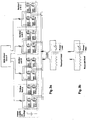
- figs. 3 and 4 The sequence control method shown on figs. 3 and 4 is related to a series compensated inverter.
- Fig. 3 shows the electrical connections. It should be observed that fig. 3a shows an example having a transformer between section outputs and the series compensated load. However, it is possible to dispense with the transformer, as indicated by fig. 3b .
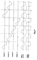
- Fig. 4 shows the current and voltage waveforms.
- the electrical connections themselves introduce necessarily nothing new, a traditional inverter can very well have the same wiring. The difference occurs in the main driver circuit, where the inverter is shared into sections which are not switched simultaneously, but follow the pattern shown on fig. 4 , which does not fall into the scope of the claims.
- Fig. 4 shows how the switching frequency of the IGBTs is lower than the resonant frequency.
- One section conducts the entire output current, but is relieved with currentless periods.
- the number of currentless periods equals the number of sections minus 1.
- the sections A - D have three currentless periods.
- the reduced switching stress allows the IGBTs to operate at much higher current levels than if the IGBTs were switched each period, like in a standard parallel operation with equal current sharing in every cycle.
- the high current operation of the IGBT secures the most effective turn off, or more precisely, the minimum turn off loss to current ratio. This increases the effectiveness of the transistors, and the output power for a given IGBT loss level increases.
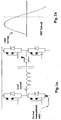
- Fig. 5 shows the enhanced maximum power output for different section numbers. This graph is based on the measurements shown in fig. 2 .
- the device suitably makes use of a new generation of NPT (Non-Punch-Through) IGBT devices from Infinion Technologies, which is designed for higher switching speed.
- NPT Non-Punch-Through
- an inverter utilizing PT (Punch-Through) IGBT's will exhibit a comparable output power increase by introducing this control strategy.
- a traditional inverter would be an inverter with one section only, and with all the IGBTs parallelled in this section. When using more than one section, parallel connection of several IGBTs within each section is a way to achieve the desired output power.
- Another possibility is a modular system where each module is a complete system as shown on fig. 3 .
- each section carries current every fourth period.
- the inverter switches each period, and the inverter output current rotates between the four sections.
- Fig. 8 presents the inventive way of arranging the switching pattern.
- all four sections conducts current in the same period, and the inverter output only switches every fourth period.
- the load current will oscillate, and power to the load is supplied by the stored energy in the oscillating LC circuit. (The load is symbolized by the variable resistor in fig. 4 .)
- the load current will decrease, as indicated in fig. 8 .
- the inverter output switches the DC link delivers power to the load and in addition enhances the stored energy in the oscillating LC circuit.
- the LC circuit thereby effectively acts as an energy storage means.
- the output voltage is defined being equal to 1 and the output current equal to 1.
- a power equal to 1 is delivered to a load impedance equal to 1.
- the output voltage then equals 1/4 and the output current equals 4.
- a power equal to 1 is delivered to a load impedance which then is 1/16.
- different switching patterns are possible. With four sections, three patterns are possible, two of them being described here. The third possibility is letting two sections carry current at a time, serving an impedance equal to 1/4.
- the present invention provides a new control strategy for IGBTs used in high frequency applications where a destressing of the IGBTs has to be performed in order to handle the switching losses.
- the strategy results inter alia in the following benefits : reduced IGBT losses; fewer IGBT chips sharing the load current; effective impedance matching property; replacing expensive custom designed MOSFET modules by standard IGBT modules ; an possibilty of utilizing similar technology for both high and low frequency applications.
- the inventive implementation of the present new control strategy will lead to a significant improvement of products in the high power high frequency product range.
- the invention also greatly outweighs the following drawbacks: increased drive circuit complexity; slightly lower efficiency compared to MOSFET inverters; using standard IGBT modules implies more free wheeling diodes than necessary for the present applications, the extra free wheeling diodes being a drawback during capacitive switching.
Landscapes
- Engineering & Computer Science (AREA)
- Power Engineering (AREA)
- Inverter Devices (AREA)
- General Induction Heating (AREA)
- X-Ray Techniques (AREA)
- Control Of High-Frequency Heating Circuits (AREA)
Claims (5)
- Hochleistungs-, Hochfrequenzresonanzlastwechselrichter-System zum Bereitstellen erhöhter Ausgangsleistung beim Betreiben einer induktiven Last in einer Induktionsheizung oder Kontaktschweißvorrichtung, wobei das System umfasst:eine Wechselrichtervorrichtung, die in Abschnitte unterteilt ist, wobei jeder Abschnitt zwei Sätze von Stromschaltern umfasst, wobei jeder Satz zwei in Reihe geschaltete Schalteinrichtungen aufweist, wobei jeder Satz an einem Mittelpunkt zwischen den Einrichtungen einen Ausgang aufweist, um einen jeweiligen Eingangsanschluss bei einer Strombelastung mit einer LC-Resonanzkompensation zu speisen, und eine Haupttreiberschaltung zum Steuern jeder Schalteinrichtung jedes Satzes, undwobei jede Schalteinrichtung ein IGBT (isolierter Gate-Bipolartransistor) ist,dadurch gekennzeichnet, dass das Wechselrichtersystem eine Arbeitsfrequenz in dem Bereich von 75 kHz - 500 kHz und eine Ausgangsleistung in dem Bereich von 10 kW - 5 MW bereitstellt;und dadurch, dass die Wechselrichtervorrichtung mit einer verringerten Schaltfrequenz, die geringer als eine LC-Resonanzfrequenz ist, arbeitet, indem Treibersignale von der Haupttreibereinheit an alle Abschnitte gleichzeitig bereitgestellt werden, um alle Abschnitte zu veranlassen, eine Stromausgabe während nur eines Zyklus der Schaltfrequenz zu liefern, wodurch alle Abschnitte veranlasst werden, eine Stromausgabe mit einer Rate 1/n der Resonanzfrequenz zu liefern, wobei n die Anzahl von Abschnitten ist.
- System nach Anspruch 1, wobei ein Netztransformator zwischen den Ausgängen und den Eingangsanschlüssen verbunden ist.
- System nach Anspruch 1 oder 2, wobei die LC-Resonanzkompensation eine LC-Reihenresonanzkompensation ist und wobei das System eine kontinuierliche sinusförmige Ausgangsspannung liefert.
- System nach Anspruch 3, wobei der gepulste Ausgang nahe und vor dem Nulldurchgang des sinusförmigen Ausgangs geschaltet ist.
- System nach Anspruch 3, wobei der Stromausgänge von allen Abschnitten addiert werden, um Schwingungen in der LC-Reihenresonanz-kompensierten Ausgangslast und somit den kontinuierlichen sinusförmigen Ausgangsstrom zu verursachen, wobei Strom mit dieser Rate der LC-Reihenresonanz-kompensierten Last zugeführt wird und somit eine pulsförmige Ausgangsspannung mit einer Rate von 1/n bereitgestellt wird.
Applications Claiming Priority (3)
| Application Number | Priority Date | Filing Date | Title |
|---|---|---|---|
| NO20004938A NO312388B1 (no) | 2000-09-29 | 2000-09-29 | Höyfrekvens vekselrettere med höy utgangseffekt og resonanslast |
| NO20004938 | 2000-09-29 | ||
| PCT/NO2001/000397 WO2002027908A1 (en) | 2000-09-29 | 2001-09-28 | High output power high frequency resonant load inverters |
Publications (2)
| Publication Number | Publication Date |
|---|---|
| EP1329017A1 EP1329017A1 (de) | 2003-07-23 |
| EP1329017B1 true EP1329017B1 (de) | 2017-03-29 |
Family
ID=19911639
Family Applications (1)
| Application Number | Title | Priority Date | Filing Date |
|---|---|---|---|
| EP01972819.5A Expired - Lifetime EP1329017B1 (de) | 2000-09-29 | 2001-09-28 | Hochfrequenzräsonanzlastwechselrichter mit hoher ausgangsleistung |
Country Status (7)
| Country | Link |
|---|---|
| US (1) | US6842355B2 (de) |
| EP (1) | EP1329017B1 (de) |
| JP (1) | JP4761696B2 (de) |
| CN (1) | CN100525052C (de) |
| AU (1) | AU2001292459A1 (de) |
| NO (1) | NO312388B1 (de) |
| WO (1) | WO2002027908A1 (de) |
Families Citing this family (17)
| Publication number | Priority date | Publication date | Assignee | Title |
|---|---|---|---|---|
| US7110897B2 (en) * | 2003-09-22 | 2006-09-19 | Tektronix, Inc. | Identification of average total loss and switching loss in duty cycle and/or frequency variation signals acquired across a switching device using a DSO |
| US7582851B2 (en) * | 2005-06-01 | 2009-09-01 | Inductotherm Corp. | Gradient induction heating of a workpiece |
| SI1917713T1 (sl) * | 2005-08-25 | 2018-11-30 | Consarc Corporation | Nadzor izhoda električnega pretvornika z modulirano impulzno širino |
| DK1870994T3 (da) * | 2006-06-23 | 2010-05-17 | Alstom Technology Ltd | Strømforsyning til elektrostatisk filter |
| DE102010033755A1 (de) * | 2010-08-09 | 2012-02-09 | Siemens Aktiengesellschaft | In Leistung und Frequenz skalierbarer Umrichter |
| US9178410B2 (en) | 2012-01-06 | 2015-11-03 | General Electric Company | Adaptive power conversion system |
| US9119592B2 (en) * | 2013-09-03 | 2015-09-01 | General Electric Company | Interleaved resonant converter |
| JP6350660B2 (ja) * | 2014-06-17 | 2018-07-04 | 株式会社明電舎 | 共振負荷用電力変換装置および共振負荷用電力変換装置の時分割運転方法 |
| JP6705234B2 (ja) * | 2015-09-29 | 2020-06-03 | 株式会社明電舎 | インバータ装置の制御方法 |
| JP6079861B1 (ja) | 2015-12-16 | 2017-02-15 | 株式会社明電舎 | 共振負荷用電力変換装置および共振負荷用電力変換装置の時分割運転方法 |
| WO2017179305A1 (ja) * | 2016-04-15 | 2017-10-19 | 株式会社明電舎 | 共振負荷用電力変換装置、共振負荷用電力変換システムにおける電力バランス制御装置、共振負荷用電力変換装置の時分割運転方法および共振負荷用電力変換システムにおける電力バランス制御方法 |
| JP6132048B1 (ja) * | 2016-04-15 | 2017-05-24 | 株式会社明電舎 | 共振負荷用電力変換装置および共振負荷用電力変換装置の時分割運転方法 |
| JP6132050B1 (ja) * | 2016-05-10 | 2017-05-24 | 株式会社明電舎 | 共振負荷用電力変換システムにおける電力バランス制御装置および電力バランス制御方法 |
| US10749443B2 (en) | 2017-01-13 | 2020-08-18 | Cree Fayetteville, Inc. | High power multilayer module having low inductance and fast switching for paralleling power devices |
| CN113767563A (zh) * | 2019-01-10 | 2021-12-07 | 沃孚半导体公司 | 用于并联功率装置的具有低电感和快速开关的高功率多层模块 |
| JP7166240B2 (ja) * | 2019-12-17 | 2022-11-07 | 株式会社東芝 | 電子回路 |
| JP7396250B2 (ja) * | 2020-11-05 | 2023-12-12 | 株式会社明電舎 | 交直変換装置および交直変換装置の制御方法 |
Citations (4)
| Publication number | Priority date | Publication date | Assignee | Title |
|---|---|---|---|---|
| US3697717A (en) * | 1971-11-19 | 1972-10-10 | Gen Electric | Induction cooking appliance with multicylinder power circuits |
| JPS5574379A (en) * | 1978-11-24 | 1980-06-04 | Sanken Electric Co Ltd | Power converter |
| DE19821993A1 (de) * | 1997-05-15 | 1998-11-19 | Fraunhofer Ges Forschung | Selbstanpassung von Gasentladungs-Speisungen |
| JPH1183906A (ja) * | 1997-09-03 | 1999-03-26 | Jeol Ltd | 誘導加熱用負荷の電流検出装置 |
Family Cites Families (13)
| Publication number | Priority date | Publication date | Assignee | Title |
|---|---|---|---|---|
| JPS5752793U (de) * | 1980-09-11 | 1982-03-26 | ||
| JPS6423589A (en) * | 1987-07-20 | 1989-01-26 | Mitsubishi Electric Corp | Method and apparatus for controlling power supply for laser |
| JP2800383B2 (ja) * | 1990-07-24 | 1998-09-21 | 富士電機株式会社 | 高周波インバータ |
| JP2734208B2 (ja) * | 1991-01-24 | 1998-03-30 | 三菱電機株式会社 | 電流形インバータ |
| JPH06104443A (ja) * | 1992-09-22 | 1994-04-15 | Fuji Electric Co Ltd | 半導体装置 |
| FR2702607B1 (fr) * | 1993-03-12 | 1995-06-09 | Electricite De France | Dispositif de commande du circuit oscillant d'un onduleur de tension fonctionnant en quasi-resonance a regulation a modulation de largeur d'impulsion. |
| US5710698A (en) * | 1994-09-30 | 1998-01-20 | Lockheed Martin Energy Systems, Inc. | Delta connected resonant snubber circuit |
| JP3221270B2 (ja) * | 1995-03-10 | 2001-10-22 | 株式会社日立製作所 | 電力変換装置及びスナバ装置 |
| US5774351A (en) * | 1996-05-21 | 1998-06-30 | National Science Council | Series resonant DC-to-AC inverter system |
| US5968398A (en) * | 1997-05-16 | 1999-10-19 | The Lepel Corporation | Apparatus and method for non-contact detection and inductive heating of heat retentive food server warming plates |
| US6078033A (en) | 1998-05-29 | 2000-06-20 | Pillar Industries, Inc. | Multi-zone induction heating system with bidirectional switching network |
| JP3761328B2 (ja) * | 1998-06-25 | 2006-03-29 | 高周波熱錬株式会社 | 誘導加熱コイル |
| US6483723B2 (en) * | 2000-11-07 | 2002-11-19 | Matsushita Electric Industrial Co., Ltd. | Switching power supply |
-
2000
- 2000-09-29 NO NO20004938A patent/NO312388B1/no not_active IP Right Cessation
-
2001
- 2001-09-28 EP EP01972819.5A patent/EP1329017B1/de not_active Expired - Lifetime
- 2001-09-28 JP JP2002531587A patent/JP4761696B2/ja not_active Expired - Fee Related
- 2001-09-28 CN CNB018164838A patent/CN100525052C/zh not_active Expired - Fee Related
- 2001-09-28 WO PCT/NO2001/000397 patent/WO2002027908A1/en not_active Ceased
- 2001-09-28 US US10/381,415 patent/US6842355B2/en not_active Expired - Lifetime
- 2001-09-28 AU AU2001292459A patent/AU2001292459A1/en not_active Abandoned
Patent Citations (4)
| Publication number | Priority date | Publication date | Assignee | Title |
|---|---|---|---|---|
| US3697717A (en) * | 1971-11-19 | 1972-10-10 | Gen Electric | Induction cooking appliance with multicylinder power circuits |
| JPS5574379A (en) * | 1978-11-24 | 1980-06-04 | Sanken Electric Co Ltd | Power converter |
| DE19821993A1 (de) * | 1997-05-15 | 1998-11-19 | Fraunhofer Ges Forschung | Selbstanpassung von Gasentladungs-Speisungen |
| JPH1183906A (ja) * | 1997-09-03 | 1999-03-26 | Jeol Ltd | 誘導加熱用負荷の電流検出装置 |
Non-Patent Citations (4)
| Title |
|---|
| DEDE E J ET AL: "On the design of a high power IGBT series resonant inverter for induction forging applications", AFRICON, 1996., IEEE AFRICON 4TH STELLENBOSCH, SOUTH AFRICA 24-27 SEPT. 1996, NEW YORK, NY, USA,IEEE, US, vol. 1, 24 September 1996 (1996-09-24), pages 206 - 211, XP010208023, ISBN: 978-0-7803-3019-1, DOI: 10.1109/AFRCON.1996.563107 * |
| DIECKERHOFF S ET AL: "Design of an IGBT-based LCL-resonant inverter for high-frequency induction heating", CONFERENCE RECORD OF THE 1999 IEEE INDUSTRY APPLICATIONS CONFERENCE. THIRTY-FORTH IAS ANNUAL MEETING (CAT. NO.99CH36370), IEEE, IEEE PISCATAWAY, NJ, USA, vol. 3, 3 October 1999 (1999-10-03), pages 2039 - 2045, XP010355091, ISBN: 978-0-7803-5589-7, DOI: 10.1109/IAS.1999.806017 * |
| MATTHES H ET AL: "1.6 MW 150 kHz Series Resonant Circuit Converter incorporating IGBT Devices for welding applications", INTERNATIONAL INDUCTION HEATING SEMINAR 1998, PADOVA,, 1 January 1998 (1998-01-01), pages 25 - 31, XP008108882 * |
| MOKHTAR KAMLI ET AL: "A 50-150 kHz Half-Bridge Inverter for Induction Heating Applications", IEEE TRANSACTIONS ON INDUSTRIAL ELECTRONICS, IEEE SERVICE CENTER, PISCATAWAY, NJ, USA, vol. 43, no. 1, 1 February 1996 (1996-02-01), XP011023146, ISSN: 0278-0046 * |
Also Published As
| Publication number | Publication date |
|---|---|
| JP4761696B2 (ja) | 2011-08-31 |
| NO20004938L (no) | 2002-04-02 |
| US20030179595A1 (en) | 2003-09-25 |
| AU2001292459A1 (en) | 2002-04-08 |
| WO2002027908A1 (en) | 2002-04-04 |
| US6842355B2 (en) | 2005-01-11 |
| CN100525052C (zh) | 2009-08-05 |
| NO20004938D0 (no) | 2000-09-29 |
| NO312388B1 (no) | 2002-04-29 |
| CN1466810A (zh) | 2004-01-07 |
| JP2004510400A (ja) | 2004-04-02 |
| EP1329017A1 (de) | 2003-07-23 |
Similar Documents
| Publication | Publication Date | Title |
|---|---|---|
| US6842355B2 (en) | High output power high frequency resonant load inverters | |
| US10630201B2 (en) | Module for a multilevel converter | |
| US5710698A (en) | Delta connected resonant snubber circuit | |
| US6069809A (en) | Resonant inverter apparatus | |
| US20120201066A1 (en) | Dual switching frequency hybrid power converter | |
| EP2117121A1 (de) | Halbleiternetzschalter | |
| US5642273A (en) | Resonant snubber inverter | |
| EP0649215A1 (de) | Halbleitervorrichtung | |
| Klumpner et al. | New solutions for a low-cost power electronic building block for matrix converters | |
| WO1991003104A1 (en) | Switching circuit employing an inductor and igbt devices | |
| EP0783203B1 (de) | Leistungswandler vom brückentyp | |
| US7253574B2 (en) | Effective switching frequency multiplier inverter | |
| US20240429833A1 (en) | Arrangement for Current Sharing of Parallel-Connected Converters | |
| US6995481B2 (en) | Energy saving electrical power control device and method | |
| RU2355531C2 (ru) | Генератор для дуговой сварки с высоким коэффициентом мощности | |
| CN113794469A (zh) | 一种倍频栅极驱动电路及其倍频控制方法 | |
| JP3793700B2 (ja) | 電力変換装置 | |
| US6266258B1 (en) | Power substrate element topology | |
| Ying et al. | High power conversion technologies & trend | |
| US6459605B1 (en) | Low inductance transistor module with distributed bus | |
| JP2000295857A (ja) | インバータ装置 | |
| Dede et al. | Switching modes and short-circuit considerations in very high frequency, very high power resonant inverters for induction heating applications | |
| JP2982364B2 (ja) | 誘導加熱用インバータ | |
| EP0713251A2 (de) | Halbleiter-Umwandlungsvorrichtung | |
| CN1091972C (zh) | 一种软开关脉宽调制电路 |
Legal Events
| Date | Code | Title | Description |
|---|---|---|---|
| PUAI | Public reference made under article 153(3) epc to a published international application that has entered the european phase |
Free format text: ORIGINAL CODE: 0009012 |
|
| 17P | Request for examination filed |
Effective date: 20030311 |
|
| AK | Designated contracting states |
Designated state(s): AT BE CH CY DE DK ES FI FR GB GR IE IT LI LU MC NL PT SE TR |
|
| AX | Request for extension of the european patent |
Extension state: AL LT LV MK RO SI |
|
| RBV | Designated contracting states (corrected) |
Designated state(s): AT BE CH CY DE ES FR GB IT LI |
|
| 17Q | First examination report despatched |
Effective date: 20090317 |
|
| GRAP | Despatch of communication of intention to grant a patent |
Free format text: ORIGINAL CODE: EPIDOSNIGR1 |
|
| RIC1 | Information provided on ipc code assigned before grant |
Ipc: H02M 7/5387 20070101AFI20161004BHEP Ipc: H02M 7/493 20070101ALI20161004BHEP Ipc: H02M 7/48 20070101ALN20161004BHEP |
|
| INTG | Intention to grant announced |
Effective date: 20161019 |
|
| RBV | Designated contracting states (corrected) |
Designated state(s): DE ES FR GB IT |
|
| GRAS | Grant fee paid |
Free format text: ORIGINAL CODE: EPIDOSNIGR3 |
|
| GRAA | (expected) grant |
Free format text: ORIGINAL CODE: 0009210 |
|
| AK | Designated contracting states |
Kind code of ref document: B1 Designated state(s): DE ES FR GB IT |
|
| REG | Reference to a national code |
Ref country code: GB Ref legal event code: FG4D |
|
| REG | Reference to a national code |
Ref country code: DE Ref legal event code: R096 Ref document number: 60150379 Country of ref document: DE |
|
| PG25 | Lapsed in a contracting state [announced via postgrant information from national office to epo] |
Ref country code: ES Free format text: LAPSE BECAUSE OF FAILURE TO SUBMIT A TRANSLATION OF THE DESCRIPTION OR TO PAY THE FEE WITHIN THE PRESCRIBED TIME-LIMIT Effective date: 20170329 |
|
| REG | Reference to a national code |
Ref country code: DE Ref legal event code: R097 Ref document number: 60150379 Country of ref document: DE |
|
| PLBE | No opposition filed within time limit |
Free format text: ORIGINAL CODE: 0009261 |
|
| STAA | Information on the status of an ep patent application or granted ep patent |
Free format text: STATUS: NO OPPOSITION FILED WITHIN TIME LIMIT |
|
| 26N | No opposition filed |
Effective date: 20180103 |
|
| REG | Reference to a national code |
Ref country code: FR Ref legal event code: ST Effective date: 20180531 |
|
| PG25 | Lapsed in a contracting state [announced via postgrant information from national office to epo] |
Ref country code: FR Free format text: LAPSE BECAUSE OF NON-PAYMENT OF DUE FEES Effective date: 20171002 |
|
| PGFP | Annual fee paid to national office [announced via postgrant information from national office to epo] |
Ref country code: IT Payment date: 20180919 Year of fee payment: 9 |
|
| PGFP | Annual fee paid to national office [announced via postgrant information from national office to epo] |
Ref country code: GB Payment date: 20180926 Year of fee payment: 18 |
|
| PGFP | Annual fee paid to national office [announced via postgrant information from national office to epo] |
Ref country code: DE Payment date: 20190917 Year of fee payment: 19 |
|
| PG25 | Lapsed in a contracting state [announced via postgrant information from national office to epo] |
Ref country code: IT Free format text: LAPSE BECAUSE OF NON-PAYMENT OF DUE FEES Effective date: 20190928 |
|
| GBPC | Gb: european patent ceased through non-payment of renewal fee |
Effective date: 20190928 |
|
| PG25 | Lapsed in a contracting state [announced via postgrant information from national office to epo] |
Ref country code: GB Free format text: LAPSE BECAUSE OF NON-PAYMENT OF DUE FEES Effective date: 20190928 |
|
| REG | Reference to a national code |
Ref country code: DE Ref legal event code: R119 Ref document number: 60150379 Country of ref document: DE |
|
| PG25 | Lapsed in a contracting state [announced via postgrant information from national office to epo] |
Ref country code: DE Free format text: LAPSE BECAUSE OF NON-PAYMENT OF DUE FEES Effective date: 20210401 |