EP1328069A2 - EMV-Vorrichtung eines drahtlosen Datenübertragungsgerätes - Google Patents
EMV-Vorrichtung eines drahtlosen Datenübertragungsgerätes Download PDFInfo
- Publication number
- EP1328069A2 EP1328069A2 EP03000409A EP03000409A EP1328069A2 EP 1328069 A2 EP1328069 A2 EP 1328069A2 EP 03000409 A EP03000409 A EP 03000409A EP 03000409 A EP03000409 A EP 03000409A EP 1328069 A2 EP1328069 A2 EP 1328069A2
- Authority
- EP
- European Patent Office
- Prior art keywords
- antenna
- lead
- coating
- enclosure
- terminal according
- Prior art date
- Legal status (The legal status is an assumption and is not a legal conclusion. Google has not performed a legal analysis and makes no representation as to the accuracy of the status listed.)
- Granted
Links
Images


Classifications
-
- H—ELECTRICITY
- H01—ELECTRIC ELEMENTS
- H01Q—ANTENNAS, i.e. RADIO AERIALS
- H01Q1/00—Details of, or arrangements associated with, antennas
- H01Q1/12—Supports; Mounting means
- H01Q1/22—Supports; Mounting means by structural association with other equipment or articles
- H01Q1/24—Supports; Mounting means by structural association with other equipment or articles with receiving set
-
- H—ELECTRICITY
- H05—ELECTRIC TECHNIQUES NOT OTHERWISE PROVIDED FOR
- H05K—PRINTED CIRCUITS; CASINGS OR CONSTRUCTIONAL DETAILS OF ELECTRIC APPARATUS; MANUFACTURE OF ASSEMBLAGES OF ELECTRICAL COMPONENTS
- H05K9/00—Screening of apparatus or components against electric or magnetic fields
- H05K9/0007—Casings
- H05K9/002—Casings with localised screening
- H05K9/0022—Casings with localised screening of components mounted on printed circuit boards [PCB]
-
- H—ELECTRICITY
- H01—ELECTRIC ELEMENTS
- H01Q—ANTENNAS, i.e. RADIO AERIALS
- H01Q1/00—Details of, or arrangements associated with, antennas
- H01Q1/12—Supports; Mounting means
- H01Q1/22—Supports; Mounting means by structural association with other equipment or articles
- H01Q1/24—Supports; Mounting means by structural association with other equipment or articles with receiving set
- H01Q1/241—Supports; Mounting means by structural association with other equipment or articles with receiving set used in mobile communications, e.g. GSM
- H01Q1/242—Supports; Mounting means by structural association with other equipment or articles with receiving set used in mobile communications, e.g. GSM specially adapted for hand-held use
- H01Q1/243—Supports; Mounting means by structural association with other equipment or articles with receiving set used in mobile communications, e.g. GSM specially adapted for hand-held use with built-in antennas
-
- H—ELECTRICITY
- H01—ELECTRIC ELEMENTS
- H01Q—ANTENNAS, i.e. RADIO AERIALS
- H01Q1/00—Details of, or arrangements associated with, antennas
- H01Q1/36—Structural form of radiating elements, e.g. cone, spiral, umbrella; Particular materials used therewith
- H01Q1/38—Structural form of radiating elements, e.g. cone, spiral, umbrella; Particular materials used therewith formed by a conductive layer on an insulating support
-
- H—ELECTRICITY
- H01—ELECTRIC ELEMENTS
- H01Q—ANTENNAS, i.e. RADIO AERIALS
- H01Q9/00—Electrically-short antennas having dimensions not more than twice the operating wavelength and consisting of conductive active radiating elements
- H01Q9/04—Resonant antennas
- H01Q9/0407—Substantially flat resonant element parallel to ground plane, e.g. patch antenna
- H01Q9/0421—Substantially flat resonant element parallel to ground plane, e.g. patch antenna with a shorting wall or a shorting pin at one end of the element
-
- H—ELECTRICITY
- H04—ELECTRIC COMMUNICATION TECHNIQUE
- H04B—TRANSMISSION
- H04B1/00—Details of transmission systems, not covered by a single one of groups H04B3/00 - H04B13/00; Details of transmission systems not characterised by the medium used for transmission
- H04B1/38—Transceivers, i.e. devices in which transmitter and receiver form a structural unit and in which at least one part is used for functions of transmitting and receiving
- H04B1/3827—Portable transceivers
- H04B1/3833—Hand-held transceivers
-
- H—ELECTRICITY
- H04—ELECTRIC COMMUNICATION TECHNIQUE
- H04B—TRANSMISSION
- H04B15/00—Suppression or limitation of noise or interference
Definitions
- the present invention relates to a shielding arrangement for a device employing wireless data transfer, such as a mobile telephone.
- the arrangement is designed to improve the EMC properties (EMC, Electromagnetic Compatibility) of the device as well as the electric properties of its antenna.
- EMC Electromagnetic Compatibility
- the width of the frequency band available to a subscriber terminal depends on many technical solutions.
- the factors affecting the width of the frequency band include the antenna structure and the structure of the components connected to the antenna.
- the antenna needs to be able to receive and transmit signals as well as possible in all circumstances.
- the frequency and power of the signal transmitted via the antenna may vary considerably depending on the device, system and circumstances, so it is of essential importance for the operation of the device that the antenna should perform optimally in all situations.
- the grounding arrangement for the antenna is also designated as "antenna ground”, which refers generally to the grounding circuitry used to establish a low-impedance connection to the earth potential or to a common reference point.
- terminals are required to be able to work at ever-higher frequencies and use more frequencies besides wider and wider frequency bands.
- the antenna structure and the components connected to it can be used as a means of determining the width of the frequency band.
- the antenna may be connected to the antenna ground by a short-circuiting conductor (short cut).
- the present invention relates especially to terminals of this category.
- the antenna must be reliable and efficient in widely varying situations and environments of application.
- the antenna may receive various spurious signals produced by the device's own electronics. Such spurious signals have an adverse effect on the duty signal, and spurious signals may appear in the conductors connected to the antenna and be passed further via the conductors to the antenna and further into the wireless transmission.
- the device itself may generate such spurious signals, some of which may be produced e.g. by harmonics associated with the clock signals of the device.
- the object of the invention is to improve the construction of a terminal so as to more effectively prevent spurious signals from being passed to the antenna or to conductors connected to the antenna.
- An additional object is to implement a device construction that allows the frequency band of the antenna of the device to be easily increased.
- the invention aims at achieving a device construction that makes it possible to improve the EMC properties of a device in a simple way.
- An additional objective is to improve the electric performance of the antenna of a device, especially to increase the frequency band of the antenna.
- a terminal employing wireless data transfer comprising an enclosure structure formed from at least one enclosure part, an antenna, and a feed conductor for receiving a signal from the antenna and/or feeding a signal into the antenna, said terminal being characterized in that it comprises a lead-in part integrated in the enclosure part and forming in the enclosure part a tubular hole through which the feed conductor is threaded to the antenna, that the said lead-in part is coated with an electrically conductive coating at least on the inner surface of the tubular hole, and that the coating is galvanically connected to the antenna ground of the device.
- the short-circuiting conductor is preferably also threaded through said hole to the antenna and galvanically connected to the antenna ground at its distant end from the antenna.
- One side of the enclosure part is preferably provided with a coating of the same material as the inner surface of the tubular hole and the coating on the enclosure part is galvanically connected to the coating on the inner surface.
- the coating is preferably on the surface of a plastic enclosure structure.
- the coating on the lead-in part is preferably connected to the antenna ground of the device via the coating on the enclosure part.
- the short-circuiting conductor and the feed conductor are preferably connected at their opposite ends from the antenna to a circuit board comprised in the device via contact surfaces formed for them.
- the contact surfaces are preferably in alignment with the tubular hole formed by the lead-in part.
- the lead-in part is preferably not completely coated with said coating.
- the short-circuiting conductor and feed conductor are formed by spring contactors.
- the lead-in part preferably forms a protrusion at least at the end pointing towards the antenna, so that the enclosure part extends closer to the antenna in the lead-in area than in the area around the lead-in part.
- the lead-in part preferably also forms a protrusion at the end opposite to the antenna, said protrusion extending outwards from the plane of the enclosure part.
- the terminal is preferably a portable subscriber terminal, preferably a mobile station.
- an enclosure part for a wireless terminal comprising a lead-in part constituting part of the same body with the enclosure part and forming a tubular hole in the enclosure part, and that the lead-in part is coated with an electrically conductive coating at least on the inner surface of the tubular hole.
- the surface of the enclosure part is preferably provided with a coating identical to that on the inner surface of the tubular lead-in hole, and that the coating on the enclosure part is galvanically connected to the coating on the inner surface.
- the principle of the invention is to integrate in the enclosure structure of the device a tubular lead-in hole that, on the one hand, functions as a shielding space and, on the other hand, increases the capacitance between the antenna and the antenna ground, thereby also increasing the frequency band of the antenna.
- the solution of the invention is also easy and economically advantageous to implement as the tubular lead-in part can be produced without separate operations and additionally the lead-in part can be coated in the same process in which the enclosure part is coated in any case.
- the connection of the feed conductor and short-circuiting conductor of the antenna is implemented using e.g. a spring contactor having good RF characteristics, then a mechanically durable connection that allows fast disconnection and causes no significant attenuation of the signal will be produced quickly and easily. Examples of this kind of spring contactors are the so-called pogo-pin type contactors.
- the lead-in part forms a protrusion at least at its end pointing towards the antenna, so that in the lead-in area the enclosure part extends closer to the antenna than in the area around the lead-in part. In this way, optimal shielding is achieved.
- Fig. 1 presents a front view of a subscriber terminal according to the invention.
- the terminal may be e.g. a mobile telephone 40 provided with keys 10 and display 20.
- the terminal may also consist of a device other than a mobile telephone because, as regards the invention, it is only essential that the device be capable of transmitting and receiving over an air interface.
- the disclosed terminal comprises an enclosure or casing structure consisting of several parts, of which the figure shows the part for the side where the display and keypad of the device are placed, i.e. the so-called A-cover 30.
- the casing structure may also be made of e.g. plastic, glass fiber or metal or a combination of these.
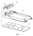
- Fig. 2 presents a subscriber terminal according to the invention in side view, showing the various parts of the enclosure structure of the device.
- the terminal presented in the figure comprises a back cover, i.e. the so-called B-cover 40 and the cover 60 of a battery space.
- the A and B covers as well as the cover of the battery space can be detached from the device structure.
- the subscriber terminal presented additionally comprises an antenna 80 placed in the battery space and a battery space cover 50.
- the antenna functioning as a radiator, may be either a so-called internal antenna or a so-called external antenna.
- the terminal comprises a circuit board 70 lodged inside the enclosure structure.
- the circuit board is placed between the A and B covers, as can be seen from the description of Fig. 3 below.
- the terminal comprises electric conductors 91 and 92 connecting the respective components on the circuit board to the antenna. As shown in the figure, the conductors 91 and 92 are passed through the B-cover from the antenna space to the circuit board.
- the antenna type of the antenna in the antenna space is actually of no importance, but the preferably the antenna is a so-called PIFA antenna (PIFA, Planar Inverted F-Antenna).
- PIFA antenna which in the case of this example is used as an internal antenna, is made of e.g. copper.
- a PIFA antenna it is possible to accomplish a particularly good radiation pattern and a low VSWR value (VSVR, Voltage Standing Wave Ratio).
- VSVR Voltage Standing Wave Ratio
- PIFA antennas are applicable for use in a relatively wide frequency band, but as stated above, increasing the frequency bandwidth is highly desirable.
- Conductor 91 is a so-called short-circuiting conductor, which short-circuits the antenna to a ground conductor 72 provided on the circuit board and functioning as antenna ground.
- the ground conductor thus represents a ground plane at earth potential, and besides being used as an antenna ground conductor it also serves as ground for the components on the circuit board.
- the length, surface area and shape of the ground conductor have an effect on the operation and properties of the antenna and the device, so the physical dimensions and shape of the ground conductor may vary considerably from case to case.
- Conductor 92 is an antenna feed conductor serving to transfer a radio-frequency information signal from the device to the antenna and from the antenna to the device. Since the antenna is made of electrically conductive material, the short-circuiting conductor 91 and the antenna feed conductor 92 are galvanically connected to each other at their ends attached to the antenna. However, these conductors are not galvanically connected to each other at their ends attached to the circuit board.
- the conductors are preferably implemented using a spring connector, so they can be at least partially compressed when the enclosure parts of the device are connected together.
- the effective length of the connection leads in the spring connector changes when they are subjected to a force acting in their longitudinal direction.
- Spring connectors also have good RF characteristics, so using them it is possible to form quickly and easily a mechanically durable connection that allows fast disconnection and causes no significant attenuation of the signal.
- Fig. 3 is an exploded view of a structure according to the invention.
- the figure shows the cover 50 of the antenna space, the B-cover 40 and the circuit board 70.
- the circuit board comprises components 71, a contact surface 93 for the short-circuiting conductor 91 and a contact surface 94 for the antenna feed conductor 92.
- the contact surface 93 of the short-circuiting conductor 91 is connected to a ground conductor 72 provided on the circuit board and serving as ground for the components as well.
- the side of the circuit board shown in Fig. 3 is the actual component side, which comprises most of the components of the circuit board.
- the circuit board is mounted with the actual component side facing towards the B-cover.
- the B-cover is provided with an electrically conductive coating on the surface facing towards the circuit board.
- this side is not necessarily coated in its entire area; instead, generally only the part that goes under the circuit board is coated.
- the dimensions and shape of the said side of the B-cover are adapted to the dimensions of the circuit board so that the circuit board and/or certain components on the circuit board will be placed in counterparts, such as cavities, formed in the B-cover 40. In this way, the circuit board is better positioned in the B-cover as lateral motion of the circuit board in relation to the surface of the B-cover is prevented.
- the antenna 89 is secured to the inner surface of the cover 50 of the antenna space.
- the figure shows the contact points 81 and 82 on the antenna to which the short-circuiting and feed conductors are connected.
- the B-cover 40 comprises a tubular lead-in part 100 formed in it for the short-circuiting and feed conductors and constituting part of the same body with the B-cover. Through the hole in the center of the lead-in part, the short-circuiting and feed conductors extend from the antenna to the contact surfaces provided for them on the circuit board.
- the lead-in part is coated with an electrically conductive material at least on its inner surface, but otherwise, in respect of its body material (under the coating) it forms a continuous body with the B-cover and is made of the same material.
- the short-circuiting and feed conductors Passing through the lead-in part, the short-circuiting and feed conductors are surrounded by electrically conductive material.
- the lead-in part and the coating on the enclosure part form a protective shield that obstructs or at least impedes the propagation of spurious signals into the conductors.
- spurious signals can not produce errors in the information signal transferred in the feed conductor 92 while it is being transferred through the feed conductor. Neither can spurious signals producing e.g. ground currents appear in the short-circuiting conductor 91 or in the ground conductor.
- the lead-in part functions as an EMC shield for signals going from the antenna towards the device, thereby reducing spurious signals affecting the components on the circuit board.
- the arrangement of the invention diminishes the propagation of spurious signals that may be produced by the components via the conductors to the antenna and further into the wireless communication.
- the end of the lead-in part 100 on the side of the antenna space protrudes from that surface 51 of the antenna space which is comprised in the B-cover and which lies opposite to the antenna space (cover) surface carrying the main part of the antenna 80.
- the aforesaid protrusion preferably reaches as close as possible to the antenna, thus providing optimal shielding of the conductors.
- the lead-in part preferably has an electrically conductive coating on both its inner and outer surfaces, whereas the rest of the surface of the lead-in part (the portion remaining inside the tube) can practically be coated on only one side, i.e. on the inner surface of the hole.
- the lead-in part provided with an electrically conductive coating changes the capacitance and inductance between the ground plane and the antenna.
- the lead-in part increases the capacitance between the antenna and the ground plane while reducing the inductance acting on the antenna feed, allowing the feed to be better adapted to the antenna than before and the frequency band of the antenna to be increased.
- Fig. 4 presents the so-called B-cover of a terminal as seen from the circuit board side.
- the lead-in part 10 has in its middle an opening or hole 101 for the feed conductor and the short-circuiting conductor, said hole going through the B-cover.
- the inner surface of the lead-in part (hole) is preferably completely coated with an electrically conductive coating material.
- the lead-in part 10 preferably protrudes from the planar surface 42 of the B-cover on this side of the B-cover as well.
- the protrusion is coated with an electrically conductive coating both on the side of the inner surface and on the side of the outer surface and also at the edge of the protrusion.
- surface 42 of the B-cover is coated with an electrically conductive coating 41 designed to prevent mutual interference between the components on the circuit board.
- the coating on the B-cover and the coating on the lead-in part 100 practically consist of the same continuous coating material because surface 42 and the lead-in part 100 are preferably coated during the same coating process.
- the protrusion on the side of the coated surface of the B-cover thus has a coating both on its inner surface and on its outer surface, so this protrusion is particularly well shielded.
- the lead-in part need not necessarily comprise a portion protruding from the surface of the B-cover; instead, the edge of the opening 101 may be level with the surface 42.
- the coating in the lead-in part and on the surface of the circuit board contains e.g. copper and stainless steel.
- the thickness of a copper coating used is typically about 1.5 ⁇ 0.5 ⁇ m and the thickness of a steel coating 0.2 ⁇ 0.1 ⁇ m.
- the coating material can be deposited on the surface of the cover e.g. by evaporating.
- Fig. 5 is a diagrammatic representation of the above-described structure when the device is ready for service.
- the circuit board comprises a ground lead 72, to which the end of the short-circuiting conductor 91, which is attached to the circuit board, is galvanically connected.
- the ground lead may be placed e.g. in an intermediate layer of a multi-layer circuit board.
- the surface of the B-cover facing towards the circuit board comprises a coating layer 41, which preferably covers the entire inner surface of the lead-in hole and which additionally continues on the other side of the hole as a coating covering the lead-in part.
- the device comprises a conductor 73 galvanically connecting the coating on the surface of the B-cover to the ground lead 72 on the circuit board.
- This conductor may be implemented in various ways, provided that a galvanic connection between the ground lead and the coating is achieved.
- the ground lead 91 and especially the feed conductor 92 do not touch the coating.
- the coating on the surface of the B-cover and the coating of the lead-in part thus form part of the device ground and antenna ground and the coatings are at earth potential, so the lead-in part gives the conductors an optimal protection against different spurious signals.
- the ground lead may be placed in different ways in the device structure; it may be placed in one or more layers of the circuit board or partly or even completely in the enclosure structure.
- a short-circuiting conductor is not absolutely necessary in all antenna structures, but the invention provides the greatest advantage in devices having an antenna provided with a short-circuiting conductor, although it is possible to achieve protection of the feed conductor and an increase of capacitance even without a short-circuiting conductor.
Applications Claiming Priority (2)
| Application Number | Priority Date | Filing Date | Title |
|---|---|---|---|
| FI20020076A FI20020076A (fi) | 2002-01-15 | 2002-01-15 | EMC-järjestely langatonta tiedonsiirtoa käyttävää laitetta varten |
| FI20020076 | 2002-01-15 |
Publications (3)
| Publication Number | Publication Date |
|---|---|
| EP1328069A2 true EP1328069A2 (de) | 2003-07-16 |
| EP1328069A3 EP1328069A3 (de) | 2003-07-30 |
| EP1328069B1 EP1328069B1 (de) | 2005-12-28 |
Family
ID=8562794
Family Applications (1)
| Application Number | Title | Priority Date | Filing Date |
|---|---|---|---|
| EP03000409A Expired - Lifetime EP1328069B1 (de) | 2002-01-15 | 2003-01-10 | EMV-Vorrichtung eines drahtlosen Datenübertragungsgerätes |
Country Status (8)
| Country | Link |
|---|---|
| US (1) | US6891505B2 (de) |
| EP (1) | EP1328069B1 (de) |
| KR (2) | KR20040081120A (de) |
| AT (1) | ATE314738T1 (de) |
| AU (1) | AU2003201177A1 (de) |
| DE (1) | DE60302909T2 (de) |
| FI (1) | FI20020076A (de) |
| WO (1) | WO2003061061A1 (de) |
Cited By (4)
| Publication number | Priority date | Publication date | Assignee | Title |
|---|---|---|---|---|
| WO2004017458A1 (en) * | 2002-08-16 | 2004-02-26 | Intel Corporation | Antenna integrated into chassis of portable device |
| EP1507313A2 (de) * | 2003-08-14 | 2005-02-16 | Nec Corporation | Antenneneinrichtung für tragbares Endgerät |
| EP2146394A1 (de) | 2008-07-15 | 2010-01-20 | Research In Motion Limited | Mobile drahtlose Kommunikationsvorrichtung mit Antennenkontakt und reduzierter RF-Induktivität |
| US7932864B2 (en) | 2008-07-15 | 2011-04-26 | Research In Motion Limited | Mobile wireless communications device with antenna contact having reduced RF inductance |
Families Citing this family (19)
| Publication number | Priority date | Publication date | Assignee | Title |
|---|---|---|---|---|
| US6585644B2 (en) * | 2000-01-21 | 2003-07-01 | Medtronic Minimed, Inc. | Ambulatory medical apparatus and method using a telemetry system with predefined reception listening periods |
| US7203549B2 (en) * | 2003-10-02 | 2007-04-10 | Medtronic, Inc. | Medical device programmer with internal antenna and display |
| US7561921B2 (en) * | 2003-10-02 | 2009-07-14 | Medtronic, Inc. | Neurostimulator programmer with internal antenna |
| US7991479B2 (en) * | 2003-10-02 | 2011-08-02 | Medtronic, Inc. | Neurostimulator programmer with clothing attachable antenna |
| US7356369B2 (en) * | 2003-10-02 | 2008-04-08 | Medtronic, Inc. | Z-axis assembly of medical device programmer |
| US20050075685A1 (en) * | 2003-10-02 | 2005-04-07 | Forsberg John W. | Medical device programmer with infrared communication |
| US7729766B2 (en) * | 2003-10-02 | 2010-06-01 | Medtronic, Inc. | Circuit board construction for handheld programmer |
| US7272445B2 (en) * | 2003-10-02 | 2007-09-18 | Medtronic, Inc. | Medical device programmer with faceplate |
| US7263406B2 (en) | 2003-10-02 | 2007-08-28 | Medtronic, Inc. | Medical device programmer with selective disablement of display during telemetry |
| US7081869B2 (en) * | 2004-10-13 | 2006-07-25 | Research In Motion Limited | Test fixture for assembled wireless devices |
| JP4300210B2 (ja) * | 2004-11-18 | 2009-07-22 | 株式会社カシオ日立モバイルコミュニケーションズ | 携帯型無線機 |
| KR100714599B1 (ko) | 2004-12-21 | 2007-05-07 | 삼성전기주식회사 | 무선통신 단말기의 내장형 안테나 조립체 |
| TW200715644A (en) * | 2005-10-14 | 2007-04-16 | Accton Technology Corp | Electronic apparatus having antenna device |
| KR200410645Y1 (ko) * | 2005-12-14 | 2006-03-09 | 고창범 | 이동통신단말기용 와이어안테나 |
| KR100798628B1 (ko) | 2006-12-27 | 2008-01-28 | 포스데이타 주식회사 | 단말기의 특성 개선 장치 |
| JP5072443B2 (ja) * | 2007-06-07 | 2012-11-14 | 株式会社東芝 | 電子機器及びその製造方法 |
| US20090231210A1 (en) * | 2008-03-13 | 2009-09-17 | Sony Ericsson Mobile Communications Ab | Portable device and battery |
| KR20100041117A (ko) * | 2008-10-13 | 2010-04-22 | 삼성전자주식회사 | 휴대용 무선 단말기의 내장형 안테나 장치 |
| TWI628993B (zh) * | 2016-09-12 | 2018-07-01 | 和碩聯合科技股份有限公司 | 背板 |
Citations (2)
| Publication number | Priority date | Publication date | Assignee | Title |
|---|---|---|---|---|
| US5617106A (en) * | 1995-04-20 | 1997-04-01 | Sierra Wireless, Inc. | Pivotable antenna and electrical device having a pivotable antenna |
| EP1102347A2 (de) * | 1999-11-17 | 2001-05-23 | Nokia Mobile Phones Ltd. | Integrierte Antennenerdungsplatte und EMV- Abschirmstruktur |
Family Cites Families (2)
| Publication number | Priority date | Publication date | Assignee | Title |
|---|---|---|---|---|
| JPH11127010A (ja) | 1997-10-22 | 1999-05-11 | Sony Corp | アンテナ装置及び携帯無線機 |
| FI114586B (fi) * | 1999-11-01 | 2004-11-15 | Filtronic Lk Oy | Tasoantenni |
-
2002
- 2002-01-15 FI FI20020076A patent/FI20020076A/fi not_active Application Discontinuation
-
2003
- 2003-01-10 DE DE60302909T patent/DE60302909T2/de not_active Expired - Lifetime
- 2003-01-10 AT AT03000409T patent/ATE314738T1/de not_active IP Right Cessation
- 2003-01-10 EP EP03000409A patent/EP1328069B1/de not_active Expired - Lifetime
- 2003-01-13 KR KR10-2004-7010754A patent/KR20040081120A/ko not_active Application Discontinuation
- 2003-01-13 KR KR1020107004680A patent/KR101037898B1/ko active IP Right Grant
- 2003-01-13 AU AU2003201177A patent/AU2003201177A1/en not_active Abandoned
- 2003-01-13 WO PCT/FI2003/000019 patent/WO2003061061A1/en active Application Filing
- 2003-01-14 US US10/341,603 patent/US6891505B2/en not_active Expired - Lifetime
Patent Citations (2)
| Publication number | Priority date | Publication date | Assignee | Title |
|---|---|---|---|---|
| US5617106A (en) * | 1995-04-20 | 1997-04-01 | Sierra Wireless, Inc. | Pivotable antenna and electrical device having a pivotable antenna |
| EP1102347A2 (de) * | 1999-11-17 | 2001-05-23 | Nokia Mobile Phones Ltd. | Integrierte Antennenerdungsplatte und EMV- Abschirmstruktur |
Cited By (6)
| Publication number | Priority date | Publication date | Assignee | Title |
|---|---|---|---|---|
| WO2004017458A1 (en) * | 2002-08-16 | 2004-02-26 | Intel Corporation | Antenna integrated into chassis of portable device |
| EP1507313A2 (de) * | 2003-08-14 | 2005-02-16 | Nec Corporation | Antenneneinrichtung für tragbares Endgerät |
| EP1507313A3 (de) * | 2003-08-14 | 2005-12-21 | Nec Corporation | Antenneneirichtung für tragbares Endgerät |
| US7342552B2 (en) | 2003-08-14 | 2008-03-11 | Nec Corporation | Antenna device for compound portable terminal |
| EP2146394A1 (de) | 2008-07-15 | 2010-01-20 | Research In Motion Limited | Mobile drahtlose Kommunikationsvorrichtung mit Antennenkontakt und reduzierter RF-Induktivität |
| US7932864B2 (en) | 2008-07-15 | 2011-04-26 | Research In Motion Limited | Mobile wireless communications device with antenna contact having reduced RF inductance |
Also Published As
| Publication number | Publication date |
|---|---|
| AU2003201177A1 (en) | 2003-07-30 |
| EP1328069A3 (de) | 2003-07-30 |
| FI20020076A0 (fi) | 2002-01-15 |
| WO2003061061A1 (en) | 2003-07-24 |
| KR20040081120A (ko) | 2004-09-20 |
| US20040100412A1 (en) | 2004-05-27 |
| EP1328069B1 (de) | 2005-12-28 |
| ATE314738T1 (de) | 2006-01-15 |
| KR20100037654A (ko) | 2010-04-09 |
| US6891505B2 (en) | 2005-05-10 |
| KR101037898B1 (ko) | 2011-05-31 |
| DE60302909T2 (de) | 2006-06-29 |
| DE60302909D1 (de) | 2006-02-02 |
| FI20020076A (fi) | 2003-07-16 |
Similar Documents
| Publication | Publication Date | Title |
|---|---|---|
| US6891505B2 (en) | EMC- arrangement for a device employing wireless data transfer | |
| US6801166B2 (en) | Planar antenna | |
| KR100903445B1 (ko) | 복수의 안테나를 갖는 무선 단말기 | |
| US6593897B1 (en) | Wireless GPS apparatus with integral antenna device | |
| US6590539B2 (en) | Antenna device in radio communication terminal | |
| KR101928989B1 (ko) | 휴대용 단말기의 안테나 장치 | |
| US6909911B2 (en) | Wireless terminal | |
| US6281850B1 (en) | Broadband multiple element antenna system | |
| US20040227674A1 (en) | Mobile communications antenna and transceiving apparatus | |
| WO2001063695A1 (en) | Compact, broadband inverted-f antennas with conductive elements and wireless communicators incorporating same | |
| EP1250725A1 (de) | Schlitzantennenanordnung | |
| EP1310014B1 (de) | Drahtloses funkgerät | |
| US6762724B2 (en) | Build-in antenna for a mobile communication terminal | |
| US6542125B1 (en) | Radio device with moveable antenna | |
| US6380898B1 (en) | Dual mode antenna and laptop carrying same | |
| JP2002152353A (ja) | 携帯端末機 | |
| KR100294189B1 (ko) | 무선전화기 내장형 마이크로스트립 패치안테나 | |
| US6297779B1 (en) | Antenna module for portable computer | |
| EP1463211A1 (de) | Tragbares Funktelefon mit reduzierter spezifischer Absorptionsrate | |
| US5920293A (en) | Radio frequency (RF) antenna coupler with an electrically extended ground plane | |
| CN113013617B (zh) | 天线组件及电子设备 | |
| CN212062680U (zh) | 新型板载蓝牙天线 | |
| US20230299482A1 (en) | Antenna device | |
| JP4421243B2 (ja) | シャーシとプリント基板から成る組合せ構造体 | |
| CN114520414A (zh) | 天线装置 |
Legal Events
| Date | Code | Title | Description |
|---|---|---|---|
| PUAI | Public reference made under article 153(3) epc to a published international application that has entered the european phase |
Free format text: ORIGINAL CODE: 0009012 |
|
| PUAL | Search report despatched |
Free format text: ORIGINAL CODE: 0009013 |
|
| AK | Designated contracting states |
Designated state(s): AT BE BG CH CY CZ DE DK EE ES FI FR GB GR HU IE IT LI LU MC NL PT SE SI SK TR |
|
| AX | Request for extension of the european patent |
Extension state: AL LT LV MK RO |
|
| AK | Designated contracting states |
Designated state(s): AT BE BG CH CY CZ DE DK EE ES FI FR GB GR HU IE IT LI LU MC NL PT SE SI SK TR |
|
| AX | Request for extension of the european patent |
Extension state: AL LT LV MK RO |
|
| RIC1 | Information provided on ipc code assigned before grant |
Ipc: 7H 05K 9/00 B Ipc: 7H 04B 1/38 B Ipc: 7H 01Q 1/24 A |
|
| RAP1 | Party data changed (applicant data changed or rights of an application transferred) |
Owner name: MICROCELL S.A., LUXEMBOURG |
|
| 17P | Request for examination filed |
Effective date: 20031017 |
|
| AKX | Designation fees paid |
Designated state(s): AT BE BG CH CY CZ DE DK EE ES FI FR GB GR HU IE IT LI LU MC NL PT SE SI SK TR |
|
| 17Q | First examination report despatched |
Effective date: 20040323 |
|
| RAP1 | Party data changed (applicant data changed or rights of an application transferred) |
Owner name: FLEXTRONICS ODM LUXEMBOURG SA, LUXEMBOURG,ZWEIGNIE |
|
| GRAP | Despatch of communication of intention to grant a patent |
Free format text: ORIGINAL CODE: EPIDOSNIGR1 |
|
| GRAS | Grant fee paid |
Free format text: ORIGINAL CODE: EPIDOSNIGR3 |
|
| GRAA | (expected) grant |
Free format text: ORIGINAL CODE: 0009210 |
|
| AK | Designated contracting states |
Kind code of ref document: B1 Designated state(s): AT BE BG CH CY CZ DE DK EE ES FI FR GB GR HU IE IT LI LU MC NL PT SE SI SK TR |
|
| PG25 | Lapsed in a contracting state [announced via postgrant information from national office to epo] |
Ref country code: IT Free format text: LAPSE BECAUSE OF FAILURE TO SUBMIT A TRANSLATION OF THE DESCRIPTION OR TO PAY THE FEE WITHIN THE PRESCRIBED TIME-LIMIT;WARNING: LAPSES OF ITALIAN PATENTS WITH EFFECTIVE DATE BEFORE 2007 MAY HAVE OCCURRED AT ANY TIME BEFORE 2007. THE CORRECT EFFECTIVE DATE MAY BE DIFFERENT FROM THE ONE RECORDED. Effective date: 20051228 Ref country code: BE Free format text: LAPSE BECAUSE OF FAILURE TO SUBMIT A TRANSLATION OF THE DESCRIPTION OR TO PAY THE FEE WITHIN THE PRESCRIBED TIME-LIMIT Effective date: 20051228 Ref country code: SK Free format text: LAPSE BECAUSE OF FAILURE TO SUBMIT A TRANSLATION OF THE DESCRIPTION OR TO PAY THE FEE WITHIN THE PRESCRIBED TIME-LIMIT Effective date: 20051228 Ref country code: LI Free format text: LAPSE BECAUSE OF FAILURE TO SUBMIT A TRANSLATION OF THE DESCRIPTION OR TO PAY THE FEE WITHIN THE PRESCRIBED TIME-LIMIT Effective date: 20051228 Ref country code: AT Free format text: LAPSE BECAUSE OF FAILURE TO SUBMIT A TRANSLATION OF THE DESCRIPTION OR TO PAY THE FEE WITHIN THE PRESCRIBED TIME-LIMIT Effective date: 20051228 Ref country code: SI Free format text: LAPSE BECAUSE OF FAILURE TO SUBMIT A TRANSLATION OF THE DESCRIPTION OR TO PAY THE FEE WITHIN THE PRESCRIBED TIME-LIMIT Effective date: 20051228 Ref country code: CH Free format text: LAPSE BECAUSE OF FAILURE TO SUBMIT A TRANSLATION OF THE DESCRIPTION OR TO PAY THE FEE WITHIN THE PRESCRIBED TIME-LIMIT Effective date: 20051228 Ref country code: NL Free format text: LAPSE BECAUSE OF FAILURE TO SUBMIT A TRANSLATION OF THE DESCRIPTION OR TO PAY THE FEE WITHIN THE PRESCRIBED TIME-LIMIT Effective date: 20051228 Ref country code: CZ Free format text: LAPSE BECAUSE OF FAILURE TO SUBMIT A TRANSLATION OF THE DESCRIPTION OR TO PAY THE FEE WITHIN THE PRESCRIBED TIME-LIMIT Effective date: 20051228 |
|
| REG | Reference to a national code |
Ref country code: GB Ref legal event code: FG4D |
|
| REG | Reference to a national code |
Ref country code: CH Ref legal event code: EP |
|
| PG25 | Lapsed in a contracting state [announced via postgrant information from national office to epo] |
Ref country code: IE Free format text: LAPSE BECAUSE OF NON-PAYMENT OF DUE FEES Effective date: 20060110 |
|
| REG | Reference to a national code |
Ref country code: IE Ref legal event code: FG4D |
|
| PG25 | Lapsed in a contracting state [announced via postgrant information from national office to epo] |
Ref country code: MC Free format text: LAPSE BECAUSE OF NON-PAYMENT OF DUE FEES Effective date: 20060131 Ref country code: LU Free format text: LAPSE BECAUSE OF NON-PAYMENT OF DUE FEES Effective date: 20060131 |
|
| REF | Corresponds to: |
Ref document number: 60302909 Country of ref document: DE Date of ref document: 20060202 Kind code of ref document: P |
|
| PG25 | Lapsed in a contracting state [announced via postgrant information from national office to epo] |
Ref country code: GR Free format text: LAPSE BECAUSE OF FAILURE TO SUBMIT A TRANSLATION OF THE DESCRIPTION OR TO PAY THE FEE WITHIN THE PRESCRIBED TIME-LIMIT Effective date: 20060328 Ref country code: BG Free format text: LAPSE BECAUSE OF FAILURE TO SUBMIT A TRANSLATION OF THE DESCRIPTION OR TO PAY THE FEE WITHIN THE PRESCRIBED TIME-LIMIT Effective date: 20060328 Ref country code: DK Free format text: LAPSE BECAUSE OF FAILURE TO SUBMIT A TRANSLATION OF THE DESCRIPTION OR TO PAY THE FEE WITHIN THE PRESCRIBED TIME-LIMIT Effective date: 20060328 |
|
| REG | Reference to a national code |
Ref country code: SE Ref legal event code: TRGR |
|
| PG25 | Lapsed in a contracting state [announced via postgrant information from national office to epo] |
Ref country code: ES Free format text: LAPSE BECAUSE OF FAILURE TO SUBMIT A TRANSLATION OF THE DESCRIPTION OR TO PAY THE FEE WITHIN THE PRESCRIBED TIME-LIMIT Effective date: 20060408 |
|
| PG25 | Lapsed in a contracting state [announced via postgrant information from national office to epo] |
Ref country code: PT Free format text: LAPSE BECAUSE OF FAILURE TO SUBMIT A TRANSLATION OF THE DESCRIPTION OR TO PAY THE FEE WITHIN THE PRESCRIBED TIME-LIMIT Effective date: 20060529 |
|
| NLV1 | Nl: lapsed or annulled due to failure to fulfill the requirements of art. 29p and 29m of the patents act | ||
| PG25 | Lapsed in a contracting state [announced via postgrant information from national office to epo] |
Ref country code: HU Free format text: LAPSE BECAUSE OF FAILURE TO SUBMIT A TRANSLATION OF THE DESCRIPTION OR TO PAY THE FEE WITHIN THE PRESCRIBED TIME-LIMIT Effective date: 20060629 |
|
| REG | Reference to a national code |
Ref country code: CH Ref legal event code: PL |
|
| REG | Reference to a national code |
Ref country code: IE Ref legal event code: MM4A |
|
| PLBE | No opposition filed within time limit |
Free format text: ORIGINAL CODE: 0009261 |
|
| STAA | Information on the status of an ep patent application or granted ep patent |
Free format text: STATUS: NO OPPOSITION FILED WITHIN TIME LIMIT |
|
| 26N | No opposition filed |
Effective date: 20060929 |
|
| EN | Fr: translation not filed | ||
| GBPC | Gb: european patent ceased through non-payment of renewal fee |
Effective date: 20070110 |
|
| PG25 | Lapsed in a contracting state [announced via postgrant information from national office to epo] |
Ref country code: GB Free format text: LAPSE BECAUSE OF NON-PAYMENT OF DUE FEES Effective date: 20070110 |
|
| PG25 | Lapsed in a contracting state [announced via postgrant information from national office to epo] |
Ref country code: FR Free format text: LAPSE BECAUSE OF FAILURE TO SUBMIT A TRANSLATION OF THE DESCRIPTION OR TO PAY THE FEE WITHIN THE PRESCRIBED TIME-LIMIT Effective date: 20070216 |
|
| PG25 | Lapsed in a contracting state [announced via postgrant information from national office to epo] |
Ref country code: EE Free format text: LAPSE BECAUSE OF FAILURE TO SUBMIT A TRANSLATION OF THE DESCRIPTION OR TO PAY THE FEE WITHIN THE PRESCRIBED TIME-LIMIT Effective date: 20051228 |
|
| PG25 | Lapsed in a contracting state [announced via postgrant information from national office to epo] |
Ref country code: TR Free format text: LAPSE BECAUSE OF FAILURE TO SUBMIT A TRANSLATION OF THE DESCRIPTION OR TO PAY THE FEE WITHIN THE PRESCRIBED TIME-LIMIT Effective date: 20051228 |
|
| PG25 | Lapsed in a contracting state [announced via postgrant information from national office to epo] |
Ref country code: FR Free format text: LAPSE BECAUSE OF FAILURE TO SUBMIT A TRANSLATION OF THE DESCRIPTION OR TO PAY THE FEE WITHIN THE PRESCRIBED TIME-LIMIT Effective date: 20060131 |
|
| PG25 | Lapsed in a contracting state [announced via postgrant information from national office to epo] |
Ref country code: CY Free format text: LAPSE BECAUSE OF FAILURE TO SUBMIT A TRANSLATION OF THE DESCRIPTION OR TO PAY THE FEE WITHIN THE PRESCRIBED TIME-LIMIT Effective date: 20051228 Ref country code: FR Free format text: LAPSE BECAUSE OF FAILURE TO SUBMIT A TRANSLATION OF THE DESCRIPTION OR TO PAY THE FEE WITHIN THE PRESCRIBED TIME-LIMIT Effective date: 20051228 |
|
| PGFP | Annual fee paid to national office [announced via postgrant information from national office to epo] |
Ref country code: DE Payment date: 20160105 Year of fee payment: 14 |
|
| PGFP | Annual fee paid to national office [announced via postgrant information from national office to epo] |
Ref country code: SE Payment date: 20160112 Year of fee payment: 14 Ref country code: FI Payment date: 20160112 Year of fee payment: 14 |
|
| REG | Reference to a national code |
Ref country code: DE Ref legal event code: R119 Ref document number: 60302909 Country of ref document: DE |
|
| PG25 | Lapsed in a contracting state [announced via postgrant information from national office to epo] |
Ref country code: FI Free format text: LAPSE BECAUSE OF NON-PAYMENT OF DUE FEES Effective date: 20170110 |
|
| PG25 | Lapsed in a contracting state [announced via postgrant information from national office to epo] |
Ref country code: DE Free format text: LAPSE BECAUSE OF NON-PAYMENT OF DUE FEES Effective date: 20170801 Ref country code: SE Free format text: LAPSE BECAUSE OF NON-PAYMENT OF DUE FEES Effective date: 20170111 |